

Page 1
Ordering number: EN2778C
CMOS LSI
LC7930N, 7930NW
LCD Drivers
Overview
The LC7930N, 7930NW are CMOS LSIs which incorporate
20-bit shift register, latch, and two sets of 20 LCD drivers.
They also have two switching pins: one of them (channel 2)
can be used as a scan-line driver (back plate) and the other
(channel 1) as a segment driver. They are optimal for LCD
interface with microcontroller (4 or 8 bits) or dot matrix
controller circuit incorporating character generator.
Features
.
Two channels of 20 output segment drivers
.
The configuration of 20 output segment drivers + 20
scanning terminal drivers available
.
A series data to connect with the microcontroller and three
control signals
.
Able to be connected in series for large display
.
Built-in bidirectional shift register can be shifted in the
direction that makes wiring easy
.
Operating supply voltage/ Operating temperature:
V
= 4.5 to 5.5 V / Topr = –20 to +75°C
DD
.
Operating current drain : IDD= 1.0 mA max
(Logic = 400 kHz, LCD = 1 kHz)
.
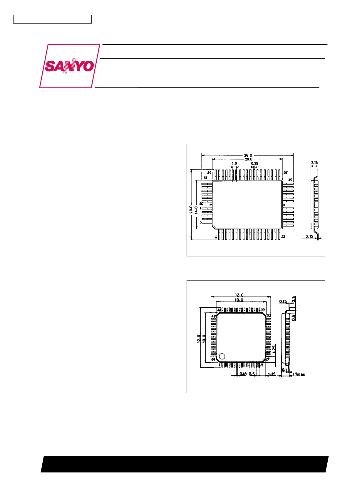
Package : Pin 60 Flat LC7930N : QIP60
Pin 64 Flat LC7930NW : SQFP64
Package Dimensions
unit : mm
3055A-QFP60C
[LC7930N]
SANYO : QIP60C
unit : mm
3190-SQFP64
[LC7930NW]
SANYO : SQFP64
SANYO Electric Co.,Ltd. Semiconductor Bussiness Headquarters
TOKYO OFFICE Tokyo Bldg., 1-10, 1 Chome, Ueno, Taito-ku, TOKYO, 110 JAPAN
13097HA(II)/12593JN/6031JN/6218TA,TS No.2778-1/7
Page 2
LC7930N, 7930NW
Specifications
Absolute Maximum Ratings atTa=25±2°C
Parameter Symbol Conditions Ratings Unit
V
max –0.3 to +7.0 V
t
t
DD
CL
SU
SL
LS
ct
DH
DD
V
max VDD–13.5 to VDD+0.3 V
EE
max
I
max
O
V
DD
Note (1) 0.7V
IH
Note (1) V
IL
CLK
CLKSR, CLK
CLK
V1, V2, V3, V4, V5, V6 V
Output transistor OFF, Y1 to Y40 V
SR
LA
SR
LDATA1, LDATA2,
RDATA1, RDATA2
CLKSR, CLK
CLKSR, CLK
CLKSR, CLK
LA
LA
LA
CLKSR→ CLK
CLKLA→ CLK
LA
SR
LDATA1, LDATA2,
RDATA1, RDATA2
–0.3 to V
EE
–0.3 to V
EE
+0.3 V
DD
to VDD+0.3 V
+0.3 V
DD
to VDD+0.3 V
4.5 5.5 V
DD
SS
0.3V
V
DD
DD
400 kHz
800 ns
800 ns
300 ns
500 ns
500 ns
200 ns
300 ns
Maximum supply voltage
Maximum input voltage V
Maximum output voltage V
Allowable power dissipation Pd max 100 mW
Operating temperature Topr –20 to +75 °C
Storage temperature Tstg –55 to +125 °C
Note : Don’t soak the whole of IC into the tank filled with melted solder for soldering
Allowable Operating Conditions at Ta = –20 to +75°C, VSS=0V,VEE=–4to–6V
Parameter Symbol Conditions min typ max Unit
Supply voltage V
High-level input voltage V
Low-level input voltage V
Shift frequency f
High-level clock width t
Low-level clock width t
Data setup time t
Clock setup time
Clock transition time t
Data retention time t
CWH
CWL
V
V
Electirical Characteristics at Ta = –20 to +75°C, VDD=+5V±10%, VSS=0V,VEE=–4to–6V
Parameter Symbol Conditions min typ max Unit
Input leakage current
I
I
High-level output voltage V
Low-level output voltage V
Vi to Yj voltage down
V
V
I
VH
Vi quiescent current
I
VL
I
DD
Supply current
I
EE
Output propagation
delay time
t
PD
Note (1): Applied to the pins; CLKSR, CLKLA, LDATA1, RDATA1, LDATA2, RDATA2, M, L/R1, L/R2, CH2-BP
(2): The equivalent circuit between Vi to Yj (i=1to6,j=1to40)
Note (1) Vin = V
IH
Note (1) Vin = V
IL
LDATA1, LDATA2,
OH
RDATA1, RDATA2
LDATA1, LDATA2,
OL
RDATA1, RDATA2
Y1 to Y40 Note (2) Ion = 100 µA, single output 1.1 V
d1
Y1 to Y40 Note (2) Ion = 50 µA, all outputs 1.5 V
d2
V1 to V6
V1 to V6
V
DD
V
EE
LDATA1, LDATA2,
RDATA1, RDATA2
DD
SS
I
= –0.4 mA VDD–0.4 V
OH
I
= 0.4 mA 0.4 V
OL
–5 µA
Open output pins
Vin=V
DD
Open output pins
Vin=V
EE
–10 µA
Open output pins
CLK
= 400 kHz
SR
Open output pins
M=1kHz
C
= 15 pF 500 ns
L
5µA
10 µA
1.0 mA
10 µA
No.2778-2/7
Page 3
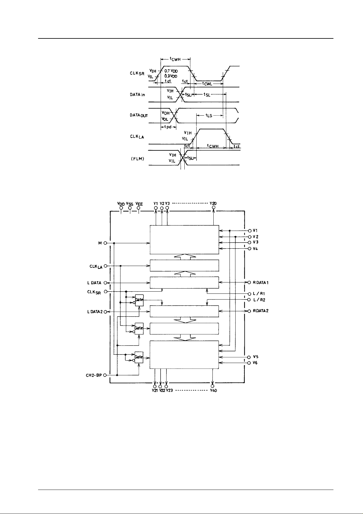
Switching Waveforms
Internal Equivalent Circuit
LC7930N, 7930NW
LCD driver
(Channel 1)
20-bit latch
20-bit bidirectional
shift register
20-bit bidirectional
shift register
20-bit latch
LCD driver
(Channel 2)
No.2778-3/7
Page 4

LC7930N, 7930NW
Pin Assignment
[LC7930N]
Number Name Input/Output Number Name Input/Output Number Name Input/Output
1 Y30 Output 21 Y14 Output 41 RDATA1 Input/Output
2 Y31 Output 22 Y13 Output 42 LDATA2 Input/Output
3 Y32 Output 23 Y12 Output 43 RDATA2 Input/Output
4 Y33 Output 24 Y9 Output 44 N.C. —
5 Y34 Output 25 Y10 Output 45 M Input
6 Y29 Output 26 Y11 Output 46 L/R1 Input
7 Y28 Output 27 Y8 Output 47 L/R2 Input
8 Y27 Output 28 Y7 Output 48 CH2-BP Input
9 Y26 Output 29 V
DD
10 Y25 Output 30 Y6 Output 50 V2 Input
11 Y24 Output 31 Y5 Output 51 V3 Input
12 Y23 Output 32 Y4 Output 52 V4 Input
13 Y22 Output 33 Y3 Output 53 V5 Input
14 Y21 Output 34 Y2 Output 54 V6 Input
15 Y20 Output 35 Y1 Output 55 Y40 Output
16 Y19 Output 36 V
17 Y18 Output 37 CLK
18 Y17 Output 38 CLK
19 Y16 Output 39 V
EE
LA
SR
SS
20 Y15 Output 40 LDATA1 Input/Output 60 Y35 Output
— 49 V1 Input
— 56 Y39 Output
Input 57 Y38 Output
Input 58 Y37 Output
— 59 Y36 Output
[LC7930NW]
Number Name Input/Output Number Name Input/Output Number Name Input/Output
1 V5 Input 23 Y6 Output 45 Y26 Output
2 V4 Input 24 V
DD
— 46 Y27 Output
3 V3 Input 25 Y7 Output 47 Y28 Output
4 V2 Input 26 Y8 Output 48 Y29 Output
5 V1 Input 27 Y11 Output 49 N.C. —
6 CH2-BP Input 28 Y10 Output 50 Y34 Output
7 L/R2 Input 29 Y9 Output 51 Y33 Output
8 L/R1 Input 30 Y12 Output 52 Y32 Output
9 M Input 31 Y13 Output 53 Y31 Output
10 RDATA2 Input/Output 32 N.C. — 54 Y30 Output
11 LDATA2 Input/OUtput 33 Y14 Output 55 N.C. —
12 RDATA1 Input/Output 34 Y15 Output 56 N.C. —
13 LDATA1 Input/Output 35 Y16 Output 57 Y35 Output
14 V
15 CLK
16 CLK
17 V
SS
SR
LA
EE
— 36 Y17 Output 58 Y36 Output
Input 37 Y18 Output 59 Y37 Output
Input 38 Y19 Output 60 Y38 Output
— 39 Y20 Output 61 Y39 Output
18 Y1 Output 40 Y21 Output 62 Y40 Output
19 Y2 Output 41 Y22 Output 63 V6 Input
20 Y3 Output 42 Y23 Output 64 N.C. —
21 Y4 Output 43 Y24 Output
22 Y5 Output 44 Y25 Output
No.2778-4/7
Page 5

LC7930N, 7930NW
Pin Descriptions
Pin Name Function
V
DD
V
SS
V
EE
Y1 to Y20 Channel 1 LCD driver output pins
Y21 to Y40 Channel 2 LCD driver output pins
V1, V2 Reference voltage for selected driver outputs
V3, V4 Reference voltage for non-selected driver outputs (channel 1)
V5, V6 Reference voltage for non-selected driver outputs (channel 2)
L/R1 Shift direction for channel 1 shift register
L/R2 Shift direction for channel 2 shift register
Logic circuitry power supply (+5 V ±10%)
0V
LCD driver power supply (–4 to –6 V)
L/R1 LDATA1 RDATA1
High-level Output Input
Low-level Input Output
L/R2 LDATA2 RDATA2
High-level Output Input
Low-level Input Output
LDATA1
RDATA1
LDATA2
RDATA2
M Switching clock signal for LCD driver.
CLK
LA
CLK
SR
CH2-BP Switches the mode of channel 2.
Serial data input/output pins for channel 1 shift register
Serial data input/output pins for channel 2 shift register
Latches channael 1 data on the falling edge.
This also will latch channel 2 data on the falling edge if CH2-BP is low.
Shift channel 1 data on the falling edge.
This also will shift channel 2 data on the falling edge if CH2-BP is low.
Exchanges the latch signal for the shift signal of channel 2 and invert the M signal.
Channel 2, then, can be used as a scan-line driver.
CH2-BP
High CLK
Low CLK
Channel 2
Latch Shift
SR
LA
CLK
CLK
LA
SR
M
M For scan-line driver
M For signal line driver
Functional Description
LC7930N, LC7930NW are serial data transfer type LCD drivers.
Data inputted serially from the data pin is shifted successively by the synchronizing clock (CLK
(CLK
.
) when the all data are shifted.
LA
Segment terminal
When CH2-BP goes to low, the data of channel 1 and channel 2 are shifted at the falling edge of CLK
the falling edge of the CLK
.
Scan terminal
. The reference pulse will be switched to selected or unselected due to the latched data.
LA
When CH2-BP goes to high, the data of channel 2 is shifted at the rising edge of CLK
the CLK
. When FLM signal, as a data, is inputted, the output will be scan terminal drive mode.
SR
SR
, and then latched at the rising edge of
LA
) and latched by the latch clock
, and then latched at
SR
Continued on next page.
No.2778-5/7
Page 6

LC7930N, 7930NW
Continued from preceding page.
(1) Waveform Diagrams for Segment Drive Mode (CH2 – BP = ‘‘L’’)
(FLM)
M
(latch)
CLK
LA
CLK
(shift)
SR
Serial input data
Latch outputs
(Y1 to Y40)
(2) Waveform Diagrams for Scan-Line/Segment Drive Mode (CH2–BP = ‘‘H’’)
LDATA2/RDATA2
(FLM)
M
CLK
(shift)
LA
CLK
(latch)
SR
Y21 to Y40
Table 1. LCD Driver Output Voltages (V1 to V6) for Y1 to Y40
CH2–BP Serial Input Data M
1
High level
(1)
Low level
(2)
(selected)
0
(un-selected)
1
0
Output
Y1 to Y20 Y21 to Y40
HV1 V2
LV2 V1
HV3 V6
LV4 V5
HV1 V1
LV2 V2
HV3 V5
LV4 V6
No.2778-6/7
Page 7

LC7930N, 7930NW
LCD Interface Examples
(Although the LCD divided voltage generator circuit is not shown here.)
(1) 40-segment bar-graph display (static)
4-bit
microcontroller
Output port
4 lines
(2) 6-digit, 7-segment + sign display. (1/3 duty cycle, 1/3 voltage bias)
3 lines
Drive controller
4-bit
microprocessor
Output port
5 lines
3 lines
(3) 20 × 60 pixel graphic display. (1/20 duty cycle, 1/5 voltage bias)
40 lines
20 lines
(3 lines/1 digit)
20 lines
20 × 60 dots
Drive controller
20 lines
8-bit
microprocessor
or
dedicated
controller
3 lines
No products described or contained herein are intended for use in surgical implants, life-support systems, aerospace equipment,
nuclear power control systems, vehicles, disaster/crime-prevention equipment and the like, the failure of which may directly or
indirectly cause injury, death or property loss.
Anyone purchasing any products described or contained herein for an above-mentioned use shall:
1 Accept full responsibility and indemnify and defend SANYO ELECTRIC CO., LTD., its affiliates, subsidiaries and distributors
and all their officers and employees, jointly and severally, against any and all claims and litigation and all damages, cost and
expenses associated with such use:
2 Not impose any responsibility for any fault or negligence which may be cited in any such claim or litigation on SANYO
ELECTRIC CO., LTD., its affiliates, subsidiaries and distributors or any of their officers and employees jointly or severally.
Information (including circuit diagrams and circuit parameters) herein is for example only; it is not guaranteed for volume
production. SANYO believes information herein is accurate and reliable, but no guarantees are made or implied regarding its use
or any infringements of intellectual property rights or other rights of third parties.
3 lines
3 lines
40 lines
This catalog provides information as of January, 1997. Specifications and information herein are subject to change without notice.
No.2778-7/7
 Loading...