

Page 1
Overview
The LC78816MB and 78816MC are 16-bit CMOS D/A
converters for use in digital audio products. They employ
a dynamic level shift conversion technique that combines
a resistor string (for the upper 9 bits), PWM (for the
middle 3 bits), and level shifting (for the lower 4 bits).
Features
• Two’s complement data format
• Two D/A converter channels built in (in-phase outputs)
• Maximum conversion frequency of 400 kHz (support for
8 times oversampling)
• Built-in output op amps
• No deglitching circuit required
• Si gate CMOS process (low power consumption)
• 5 V single-voltage power supply
• Low voltage (3.5 V) operation possible
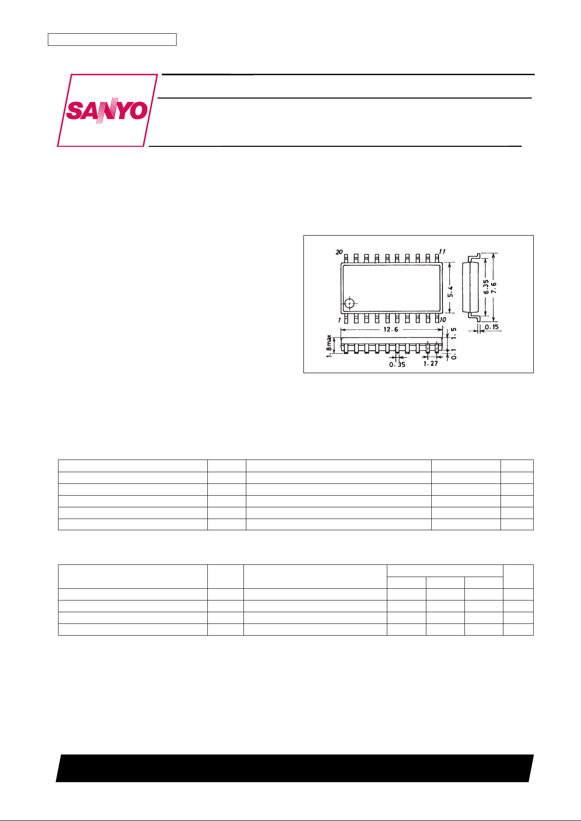
Package Dimensions
unit: mm
3036B-MFP20
CMOS LSI
63096HA (OT)/D1694TH(OT)/61893JN No. 4250-1/11
Preliminaly
SANYO: DIP20
[LC78816MB, 78816MC]
SANYO Electric Co.,Ltd. Semiconductor Bussiness Headquarters
TOKYO OFFICE Tokyo Bldg., 1-10, 1 Chome, Ueno, Taito-ku, TOKYO, 110 JAPAN
16-Bit D/A Converter for Use in
Digital Audio Products
LC78816MB, 78816MC
Ordering number : EN*4250C
Parameter Symbol Conditions Ratings Unit
Maximum power supply voltage V
DD
max –0.3 to +7.0 V
Input voltage V
IN
–0.3 to VDD+ 0.3 V
Output voltage V
OUT
–0.3 to VDD+ 0.3 V
Operating temperature Topr –30 to +75 °C
Storage temperature Tstg –40 to +125 °C
Specifications
Absolute Maximum Ratings at Ta = 25°C
Parameter Symbol Conditions
Ratings
Unit
min typ max
Power supply voltage V
DD
3.5 5.0 5.5 V
Reference voltage high V
refH
VDD– 0.3 V
DD
V
Reference voltage low V
refL
0 0.3 V
Operating temperature Topr –30 +75 °C
Allowable Operating Ranges
Page 2
No. 4250-2/11
LC78816MB, 78816MC
Parameter Symbol Conditions
Ratings
Unit
min typ max
Input high level voltage (1) V
IH
Input pins other than SYSCLK 2.2 V
Input low level voltage (1) V
IL
Input pins other than SYSCLK 0.8 V
Input high level voltage (2) V
IH
The SYSCLK pin 0.7 V
DD
V
Input low level voltage (2) V
IL
The SYSCLK pin 0.3 V
DD
V
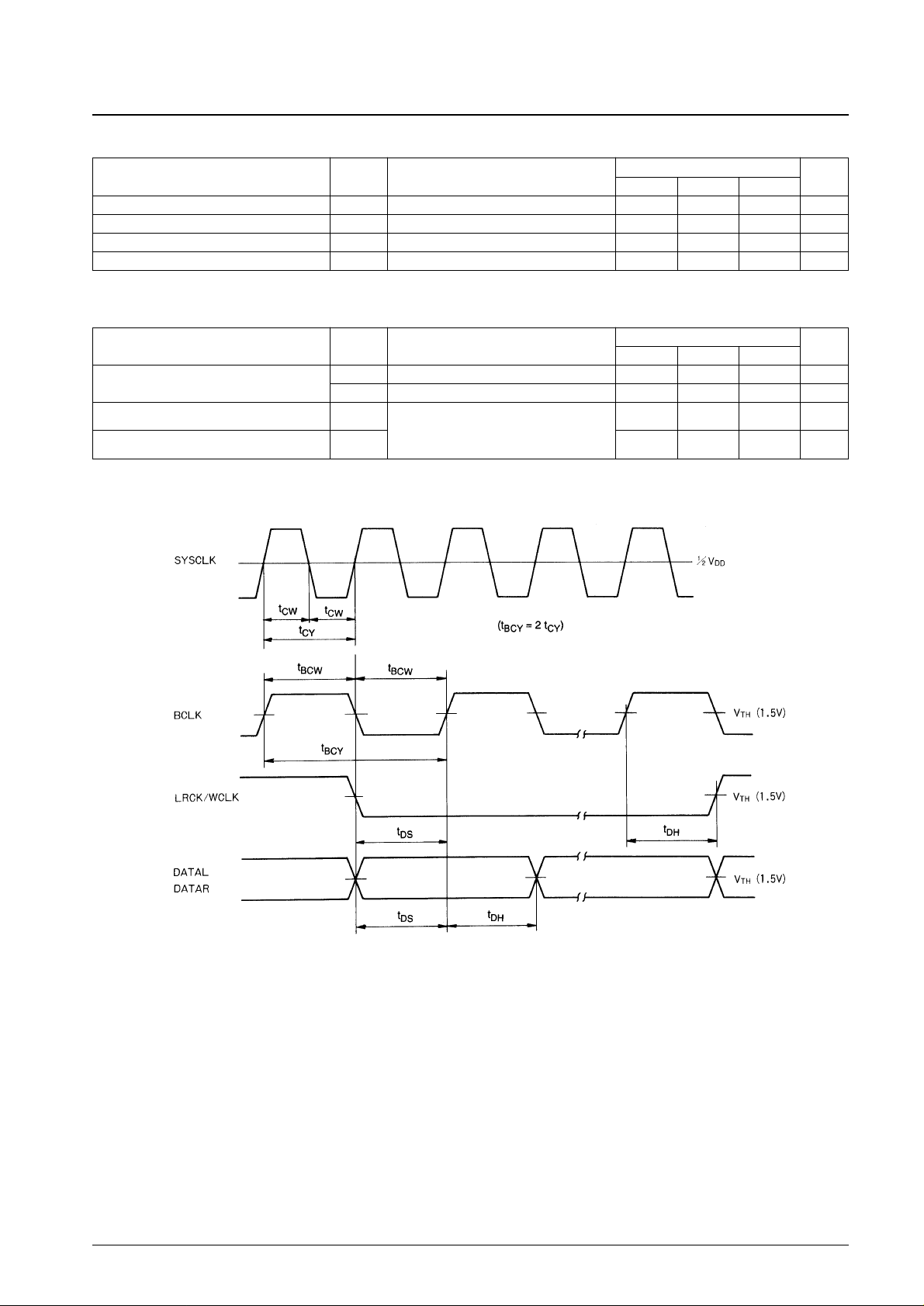
DC Characteristics at Ta = –30 to +75°C, VDD= 3.5 to 5.5 V, VSS= 0 V
Parameter Symbol Conditions
Ratings
Unit
min typ max
Clock pulse width
t
CW
SYSCLK 25 ns
t
BCW
BCLK 35 ns
Setup time t
DS
LRCK/WCLK
20 ns
Hold time t
DH
DATAL
20 ns
DATAR
AC Characteristics at Ta = –30 to +75°C, VDD= 3.5 to 5.5 V, VSS= 0 V
Page 3
No. 4250-3/11
LC78816MB, 78816MC
Parameter Symbol Conditions
Ratings
Unit
min typ max
Resolution RES 16 Bits
Conversion frequency fs 400 kHz
Total harmonic distortion THD1 LC78816MB at 1 kHz, 0 dB 0.05* %
Total harmonic distortion THD1 LC78816MC at 1 kHz, 0 dB 0.08 %
Dynamic range D
R
At 1 kHz, –60 dB 94 96 dB
Cross talk C · T At 1 kHz, 0 dB –85 dB
Signal to noise ratio S/N JIS-A 96 dB
Full scale output voltage VFS 3.0 3.3 3.5 Vp-p
Power dissipation Pd 35 60 mW
Output load resistance R
L
Pins 1 and 20 5 kΩ
Electrical Characteristics (1) at Ta = 25°C, DVDD= AVDD= V
refH
= 5.0 V, DGND = AGND = V
refL
= 0.0 V
Notes:*: Screened units
Test circuit: based on the sample application circuit, with a sampling frequency (fs) of 88.2 kHz.
Parameter Symbol Conditions
Ratings
Unit
min typ max
Resolution RES 16 Bits
Conversion frequency fs 400 kHz
Total harmonic distortion THD1 LC78816MB at 1 kHz, 0 dB 0.06* %
Total harmonic distortion THD1 LC78816MC at 1 kHz, 0 dB 0.09 %
Dynamic range D
R
At 1 kHz, –60 dB 92 94 dB
Cross talk C · T At 1 kHz, 0 dB –85 dB
Signal to noise ratio S/N JIS-A 96 dB
Full scale output voltage VFS 2.0 2.3 2.5 Vp-p
Power dissipation Pd 10 20 mW
Output load resistance R
L
Pins 1 and 20 15 kΩ
Electrical Characteristics (2) at Ta = 25°C, DVDD= AVDD= V
refH
= 5.0 V, DGND = AGND = V
refL
= 0.0 V
Notes:*: Screened units
Test circuit: based on the sample application circuit, with a sampling frequency (fs) of 88.2 kHz.
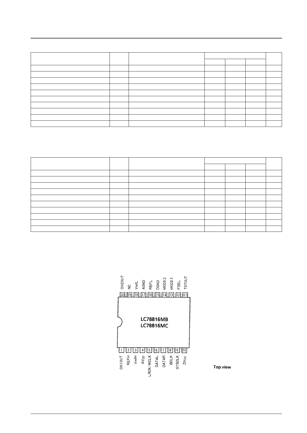
Pin Assignment
Page 4
No. 4250-4/11
LC78816MB, 78816MC
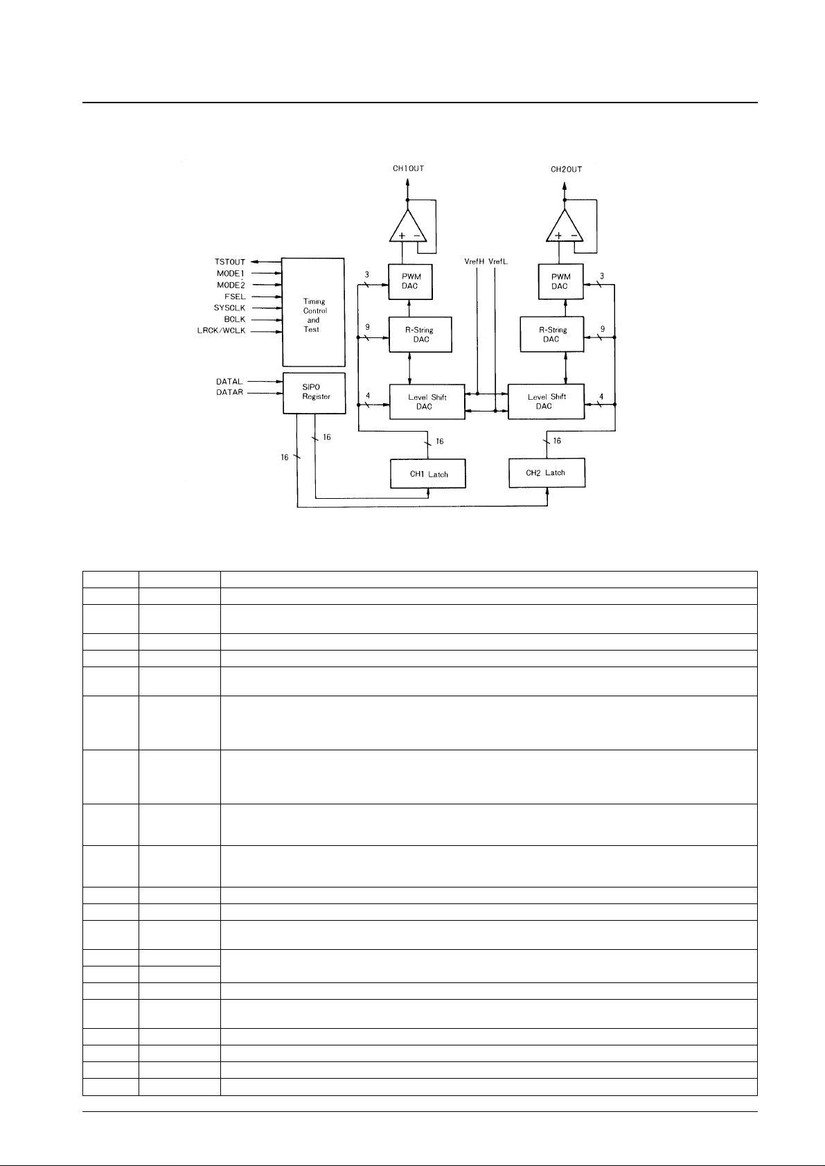
Block Diagram
Pin No. Pin Name Function and Operational Description
1 CH1OUT Channel 1 output pin (left channel)
2
REFH
Reference voltage high level pin
Normally connected to AGND through a capacitor.
3 VrefH Reference voltage high level input pin
4 AV
DD
Analog system power supply voltage pin
5
LRCK/WCLK
LR clock and word clock input pin
Used to generate the internal signal that latches the digital audio data (DATAL and DATAR).
Digital audio data input pin
6 DATAL
Data is input from the MSB bit serially.
When FSEL is low, channel 1 data is input.
When FSEL is high, channel 1 and channel 2 data are input using time division.
Digital audio data input pin
7 DATAR
Data is input from the MSB bit serially.
When FSEL is low, channel 2 data is input.
When FSEL is high, functions as the interface switching pin.
Bit clock input pin
8 BCLK This is the clock for reading in digital audio data bit serially. Also functions as the IC’s system clock when SYSCLK is
fixed low or high.
System clock input pin
9 SYSCLK This is the system clock that drives the IC. However, in certain modes it is used as the interface switching pin.
(See the timing charts.)
10 DV
DD
Digital system power supply voltage pin
11 TSTOUT Output pin for IC testing
12 FSEL
When low, digital audio data is input simultaneously from the DATAL and DATAR pins.
When high, digital audio data is input from the DATAL pin in time division mode.
13 MODE1
Interface switching pins. (See the timing charts.)
14 MODE2
15 DGND Digital system ground pin
16 REFL
Reference voltage low level pin.
Normally connected to AGND through a capacitor.
17 AGND Analog system ground pin
18 VrefL Reference voltage low level input pin
19 NC No connection
20 CH2OUT Channel 2 output pin (right channel)
Pin Functions
Page 5

No. 4250-5/11
LC78816MB, 78816MC
Operation
(1) Input of digital audio data
Digital audio data is a 16-bit serial signal in an MSB first two’s complement format.
The 16-bit serial data is read into the IC from MSB on the rising edge of the BCLK signal.
The LC78816MB and 78816MC can handle various interface types.
See the timing charts for details.
DSP ICs for CD players: See timing chart (1)-① when interfacing with the LC7868KE or the 7869E.
(2) Converter operation (See Figure 1.)
The LC78816MB and 78816MC have independent D/A converter circuits for channel 1 and channel 2. These D/A
converters use a dynamic level shift conversion technique that combines resistor string (R-string DAC), PWM (pulse
width modulation), and level shifting D/A converters. After latching, the 16-bit input digital audio data (D15to D0) is
sent to these separate D/A converters as follows:
Upper 9 bits (D15to D7): To the R-string DAC.
Middle 3 bits (D6to D4): To the PWM DAC.
Lower 4 bits (D3to D0): To the level shifting DAC.
① R-string DAC
The resistor string D/A converter consists of 512 (29) unit resistances (R) connected in series. The voltage applied at
the terminals of this resistor string is divided into 512 equal divisions to form the 9-bit D/A converter outputs.
The upper 9 bits of the input data value are used to select (using a switching circuit) two adjacent potentials, V1 and
V2, from the divided voltages. These are output to the PWM DAC. The relationship between these two voltages is
given by the following formula:
V2 – V1 = (VH – VL)/512
② PWM DAC
The PWM DAC is a 3-bit D/A converter that divides the interval between the two voltages, V1 and V2 output by the
R-string DAC, into 8 using PWM (pulse width modulation).
Either V1 or V2, depending on the value of the middle three bits of the data, is output to the CH1OUT (or CH2OUT)
pin.
SYSCLK is used for the PWM clock when timing chart (2)-② and (2)-③ are used, and BCLK is used for all other
timing charts.
③ Level Shift DAC
Two variable resistors, VRH and VRL, are connected in series at the ends of the R-string DAC resistor string to
implement a 4-bit D/A converter circuit. The variable resistors VRH and VRL operate as follows in response to the
lower 4 bits of the data value.
• Independent of the data value, the sum of the resistances (VRH + VRL) remains constant.
• According to the data value, VRH and VRL vary in the range from 0 to 15R/128 (where R is the value of the
resistors in the R-string DAC) in steps of R/128.
As a result, the R-string DAC outputs V2 and V1 vary according to the lower 4 bits of the data in steps of ∆V/128
over a range 0 to 15 × ∆V/128 (where ∆V = (VH – VL)/512).
Page 6

No. 4250-6/11
LC78816MB, 78816MC
D/A Conversion Technique Used in the LC78816MB and 78816MC
Figure 1 D/A Conversion Technique Used in the LC78816MB and 78816MC
V
ref
pins (See Figure 1.)
The V
ref
pins that provide the reference voltages for the resistor string are normally set at V
refH
= 5 V and V
refL
= 0 V.
Also, a capacitor of about 47 µF should be connected between REFH and AGND, and another between REFL and
AGND. As a result of the built-in resistors RH and RL, the maximum output amplitude of the LC78816MB and
78816MC is in a range of 0.5 V (min) to 3.8 V (max) (3.3 Vp-p) for 0 dB playback.
Page 7

Timing Charts
No. 4250-7/11
LC78816MB, 78816MC
(1) For time division input of the CH1 and CH2 data (FSEL = high)
(1)-① MODE1 = “L”, MODE2 = “L”, FSEL = “H”
DATAR = “L”
SYSCLK = “L”
(1)-② MODE1 = “L”, MODE2 = “H”, FSEL = “H”
When SYSCLK = “L”: “LRCK/WCLK
1
”, when “H”: “LRCK/WCLK
2
”
When DATAR = “L”: “DATAL
1
”, when “H”: “DATAL
2
”
Page 8

No. 4250-8/11
LC78816MB, 78816MC
Timing Charts
(1)-③ MODE1 = “H”, MODE2 = “L”, FSEL = “H”
When SYSCLK = “L”: “LRCK/WCLK
1
”, when “H”: “LRCK/WCLK
2
”
When DATAR = “L”: “DATAL
1
”, when “H”: “DATAL
2
”
Page 9

Timing Charts
No. 4250-9/11
LC78816MB, 78816MC
(1)-④ MODE1 = “H”, MODE2 = “H”, FSEL = “H”
When SYSCLK = “L”: “LRCK/WCLK
1
”, when “H”: “LRCK/WCLK
2
”
When DATAR = “L”: “DATAL
1
”, when “H”: “DATAL
2
”
(2) For simultaneous input of CH1 and CH2 data (FSEL = low)
(2)-① MODE1 = “L”, MODE2 = “L”, FSEL = “L”
When SYSCLK = “L”: “LRCK/WCLK
1
”, when “H”: “LRCK/WCLK
2
”
Page 10

Timing Charts
No. 4250-10/11
LC78816MB, 78816MC
(2)-② MODE1 = “L”, MODE2 = “H”, FSEL = “L”
(2)-③ MODE1 = “H”, MODE2 = “H”, FSEL = “L”
Page 11

No. 4250-11/11
LC78816MB, 78816MC
Sample Application Circuit
This catalog provides information as of December, 1997. Specifications and information herein are subject to
change without notice.
■ No products described or contained herein are intended for use in surgical implants, life-support systems, aerospace
equipment, nuclear power control systems, vehicles, disaster/crime-prevention equipment and the like, the failure of
which may directly or indirectly cause injury, death or property loss.
■ Anyone purchasing any products described or contained herein for an above-mentioned use shall:
➀ Accept full responsibility and indemnify and defend SANYO ELECTRIC CO., LTD., its affiliates, subsidiaries and
distributors and all their officers and employees, jointly and severally, against any and all claims and litigation and all
damages, cost and expenses associated with such use:
➁ Not impose any responsibility for any fault or negligence which may be cited in any such claim or litigation on
SANYO ELECTRIC CO., LTD., its affiliates, subsidiaries and distributors or any of their officers and employees
jointly or severally.
■ Information (including circuit diagrams and circuit parameters) herein is for example only; it is not guaranteed for
volume production. SANYO believes information herein is accurate and reliable, but no guarantees are made or implied
regarding its use or any infringements of intellectual property rights or other rights of third parties.
Notes: 1. DVDDand DGND must be connected to the digital system power supply, and AVDDand AGND to the analog system power supply.
2. Use a low impedance high stability power supply (a unit equivalent to a commercial three terminal regulator) for V
DD
and VrefH.
3. Since latchup is possible if there is a discrepancy between the power supply rise times for pin 4 (AV
DD
) and pin 10 (DVDD), design the system so
that there is no time lag between the pin 4 and pin 10 power application times.
 Loading...