

Page 1
Ordering number : EN4868A
O3097HA (OT)/20695TH (OT) No. 4868-1/17
SANYO Electric Co.,Ltd. Semiconductor Bussiness Headquarters
TOKYO OFFICE Tokyo Bldg., 1-10, 1 Chome, Ueno, Taito-ku, TOKYO, 110 JAPAN
CD Graphics Decoder
LC7872E
CMOS LSI
Overview
The LC7872E is a CMOS LSI that integrates in a single
chip the signal processing functions required for compact
disk graphics (CD-G) decoding. The LC7872E accepts the
subcode R to W signals output by a CD-DSP chip such as
the Sanyo LC786X series, LC7862XE series or
LC7863XE series and performs de-interleaving, error
detection and correction, graphics instruction processing
and image processing.
Functions
• Built-in RGB encoder allows a CD-G decoder to be
implemented in just two chips: the LC7872E and an
external 64-kword × 4-bit DRAM
• Interpolation and protection for the CD subcode
synchronization signals as well as de-interleaving, error
detection and correction for the R to W signals.
• Two crystal oscillator systems, one for NTSC and one
for PAL are provided and can be switched easily using
the control pin provided. The standard clock and all
required internal timings can be generated by
connecting a 14.31818 MHz crystal for NTSC and/or a
17.734476 MHz crystal for PAL.
• The LC7872E performs CD graphics instruction
processing and drawing processing and controls the
image display.
• Composition video 8-bit D/A converter output provided
• Superimposition support
• Microprocessor interface provided to support set
upgrades.
• Define transparency support
• Color bar output function
Features
• A CD-G decoder can be implemented with just two
chips: a controller is not required.
• Silicon gate CMOS structure for low power operation
• Single 5 V power supply
• 64-pin QFP (QIP) package
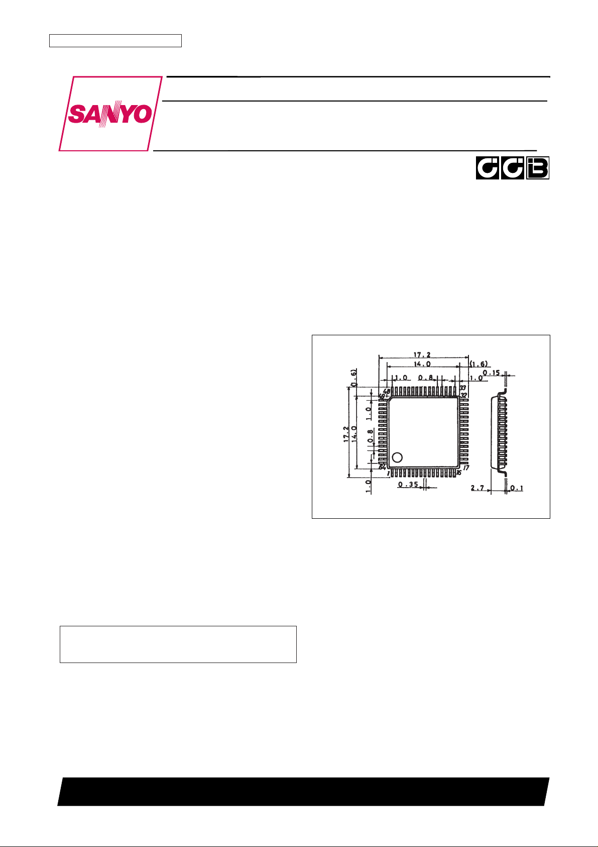
Package Dimensions
unit: mm
3159-QFP64E
• CCB is a trademark of SANYO ELECTRIC CO., LTD.
• CCB is SANYO’s original bus format and all the bus
addresses are controlled by SANYO.
[LC7872E]
SANYO: QFP64E
Page 2
Block Diagram
Pin Assignment
No. 4868-2/17
LC7872E
Microcontroller
interface
DB0 to DB3
A0 to A7
TRANS0 to TRANS5
Page 3
Specifications
Absolute Maximum Ratings at Ta = 25°C, VSS= 0 V
Allowable Operating Ranges at Ta = 25°C, VSS= 0 V
Electrical Characteristics at Ta = 25°C, VSS= 0 V, VDD= 5 V
No. 4868-3/17
LC7872E
Parameter Symbol Conditions Ratings Unit
Maximum supply voltage V
DD
max VSS– 0.3 to +7.0 V
Maximum input voltage V
IN
max VSS– 0.3 to VDD+ 0.3 V
Maximum output voltage V
OUT
max VSS– 0.3 to VDD+ 0.3 V
Allowable power dissipation Pd max 300 mW
Operating temperature Topr –30 to +85 °C
Storage temperature Tstg –40 to +125 °C
Parameter Symbol Conditions min typ max Unit
Supply voltage V
DD
VDD1, VDD2 4.5 5.5 V
V
IH
(1) RESET 0.7 V
DD
V
DD
V
Input high level voltage
V
IH
(2)
SFSY, PW, SBSY, CE, DI, CL, MUTE, DB0 to DB3,
2.2 V
DD
V
PALID, HRESET, VRESET, N/P1, N/P2, SON
V
IH
(3) S1, S2, CB, TEST, TEST1, LINE, DEN 0.8 V
DD
V
DD
V
V
IL
(1) RESET V
SS
0.3 V
DD
V
Input low level voltage
V
IL
(2)
SFSY, PW, SBSY, CE, DI, CL, MUTE, DB0 to DB3,
V
SS
0.8 V
PALID, HRESET, VRESET, N/P1, N/P2, SON
V
IL
(3) S1, S2, CB, TEST, TEST1, LINE, DEN V
SS
0.2 V
DD
V
High level clock pulse width t
øH
CL: Figure 1 400 ns
Low level clock pulse width t
øL
CL: Figure 1 400 ns
Data setup time t
DS
CL, DI: Figure 1 200 ns
Data hold time t
DH
CL, DI: Figure 1 200 ns
CE wait time t
CP
CE, CL: Figure 1 400 ns
CE setup time t
CS
CE, CL: Figure 1 400 ns
CE hold time t
CH
CE, CL: Figure 1 400 ns
DO setup time t
DOS
CL, DO: Figure 1 130 300 ns
fin (1) XIN1 14.31818 MHz
fin (2) XIN2 17.734476 MHz
Input frequency fin (3) 4FSC2
NTSC mode 14.31818 MHz
PAL mode 17.734476 MHz
fin (4) FSCIN
NTSC mode 3.58 MHz
PAL mode 4.43 MHz
Input amplitude V
IN
XIN1, XIN2, 4FSC2, FSCIN:
0.3 5 Vp-p
sine wave, capacitive coupling
Reset pulse width t
WRES
RESET 400 ns
Parameter Symbol Conditions min typ max Unit
Current drain
I
DD
(1) VDD1 24 40 mA
I
DD
(2) VDD2 12 20 mA
S1, S2, SFSY, PW, SBSY, CE, DI, CL, MUTE, LINE,
Input high level current
IIH(1) HRESET, VRESET, N/P1, N/P2, RESET, SON: 5 µA
V
IN
= V
DD
IIH(2) CB, TEST, TEST1, DEN: VIN= V
DD
30 100 200 µA
S1, S2, SFSY, PW, SBSY, CE, DI, CL, MUTE, LINE,
Input low level current
VIL(1) HRESET, VRESET, N/P1, N/P2, RESET, SON: –5 µA
V
IN
= V
SS
VIL(2) PALID: VIN= V
SS
–200 –100 –30 µA
SBCK, WE, RAS, CAS, OE, A0 to A7, DB0 to DB3,
Output high level voltage V
OH
CDGM, TRANS0 to TRANS5, VSYNC, YS, CSYNC, VDD– 1 V
DD
V
EFLG, FSX, FSC: I
O
= –0.5 mA
Continued on next page.
Page 4
Continued from preceding page.
No. 4868-4/17
LC7872E
Parameter Symbol Conditions min typ max Unit
SBCK, WE, RAS, CAS, OE, A0 to A7, DB0 to DB3,
Output low level voltage
VOL(1) CDGM, TRANS0 to TRANS5, VSYNC, YS, CSYNC, V
SS
0.4 V
EFLG, FSX, FSC: I
O
= 2 mA
V
OL
(2) DO: IO= 5 mA V
SS
0.75 V
Output off leakage current I
OFF
DO, DB0 to DB3 –5 +5 µA
Built-in feedback resistance R
X
XIN1, XIN2, 4FSC2, FSCIN 1 MΩ
8-bit D/A converter
V
REF
VIDEO 2.40 2.45 2.50 V
reference voltage
8-bit D/A converter
R
DA
VIDEO 300 Ω
output resistance
8-bit D/A converter output level V
DAC
VIDEO: Figure 9
Random read/write cycle time t
RC
Figures 2 and 3 250 ns
Page mode cycle time t
PC
Figures 4 and 5 130 ns
RAS access time t
RAC
Figure 2 210 ns
CAS access time t
CAC
Figures 2 and 4 10 ns
Output turn-off delay time t
OFF
Figures 2 and 4 20 ns
RAS precharge time t
RP
Figures 2, 3, 4, 5 and 6 100 ns
RAS pulse width t
RAS
Figures 2, 3 and 6 120 ns
RAS pulse width (page mode) t
RASP
Figures 4 and 5 18000 ns
RAS hold time t
RSH
Figures 2, 3, 4 and 5 60 ns
CAS hold time t
CSH
Figures 2 and 3 120 ns
CAS pulse width t
CAS
Figures 2, 3, 4 and 5 60 ns
CAS precharge time t
CPN
Figure 6 50 ns
CAS precharge time (page mode) t
CP
Figures 4 and 5 50 ns
Row address setup time t
ASR
Figures 2, 3, 4 and 5 100 ns
Row address hold time t
RAH
Figures 2, 3, 4 and 5 50 ns
Column address setup time t
ASC
Figures 2, 3, 4 and 5 0 ns
Column address hold time t
CAH
Figures 2, 3, 4 and 5 50 ns
Read command setup time t
RCS
Figure 2 150 ns
Read command hold time
t
RCH
Figure 2 120 ns
(referenced to CAS)
Read command hold time
t
RRH
Figure 2 120 ns
(referenced to RAS)
Write command setup time t
WCS
Figure 3 100 ns
Write command hold time t
WCH
Figure 3 50 ns
Write command pulse width t
WP
Figure 3 150 ns
Write data setup time t
DS
Figure 3 100 ns
Write data hold time t
DH
Figure 3 100 ns
CAS setup time (CAS before RAS) t
CSR
Figure 6 50 ns
CAS hold time (CAS before RAS) t
CHR
Figure 6 50 ns
RAS precharge · CAS active time t
RPC
Figure 6 50 ns
Video setup time t
VS
Superimposition: Figure 7 20 25 ns
SBCK output delay time t
SD
NTSC mode: Figure 8 4.74 5.03 µs
PAL mode: 4.79 5.08 µs
SBCK cycle frequency f
SC
NTSC mode: Figure 8 224 kHz
PAL mode: 222 kHz
PW setup time t
PWS
Figure 8 100 ns
Page 5
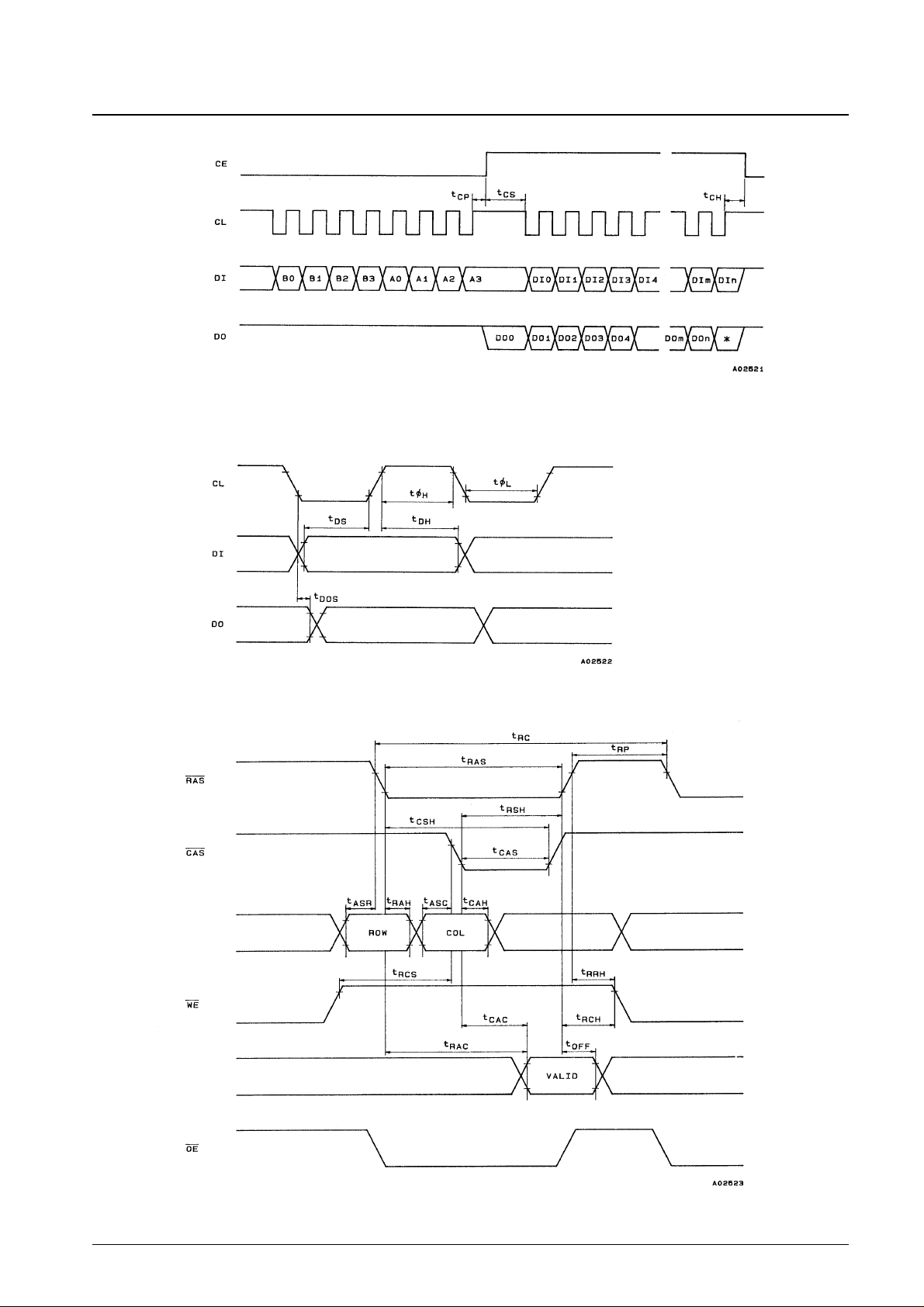
Figure 1 Microcontroller Interface Timing
Figure 2 DRAM Read Cycle
No. 4868-5/17
LC7872E
A0 to A7
DB0 to DB3
Page 6
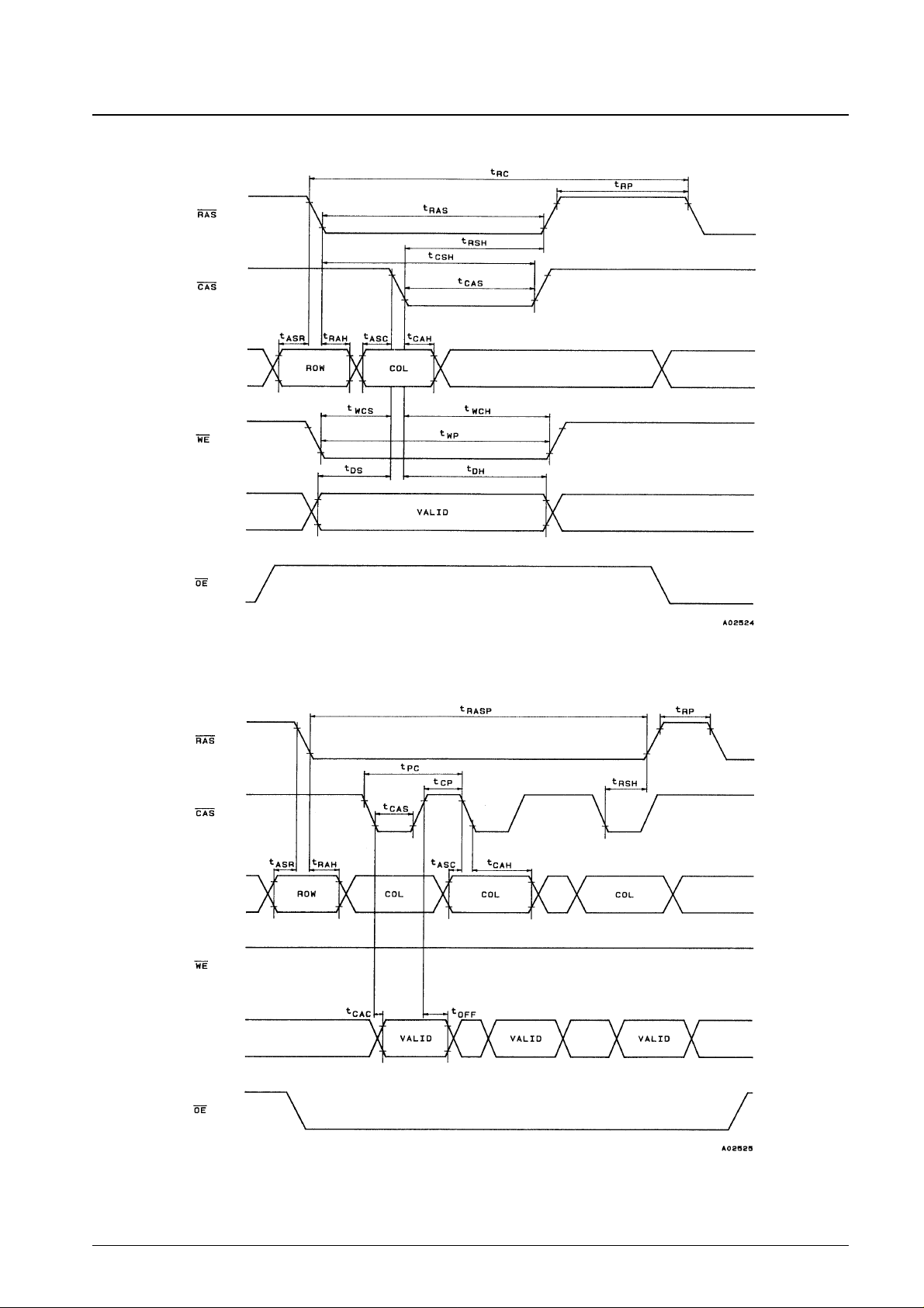
Figure 3 DRAM Early Write Cycle
Figure 4 DRAM Page Mode Read Cycle
No. 4868-6/17
LC7872E
A0 to A7
DB0 to DB3
A0 to A7
DB0 to DB3
Page 7

Figure 5 DRAM Page Mode Write Cycle
Figure 6 DRAM CAS before RAS Refresh Cycle
Figure 7 Phase Relationships in Superimposition Mode
No. 4868-7/17
LC7872E
A0 to A7
DB0 to DB3
Page 8

Figure 8 Subcode Interface
Figure 9 Composite Video 8-Bit Digital Values (Color Bar Output) at VDD2 = 5 V
No. 4868-8/17
LC7872E
Pin S1 = Pin S2 = High
Page 9

Pin Functions
No. 4868-9/17
LC7872E
Pin No. Symbol I/O Function
1 S1 I
S1 S2 CD DSP
CD DSP selection
0 0 LC7861N/67
2 S2 I
1 0 LC7860K/63
1 1 LC7868/69/681
3 SBCK O Subcode R to W readout clock
4 SFSY I Subcode frame synchronization signal
5 PW I Subcode R to W data
6 SBSY I Subcode block synchronization signal
7 V
DD
1 — Digital system power supply
8 CE I Serial input or control pin during serial output
9 DO O Serial data output (N-ch open drain)
10 DI I Serial data input
11 CL I Serial data I/O clock
12 MUTE I Control signal that invalidates the subcode data
13 V
SS
1 — Digital system ground
14 WE O DRAM control
15 RAS O DRAM control
16 A0 O DRAM address
17 A1 O DRAM address
18 A2 O DRAM address
19 A3 O DRAM address
20 A4 O DRAM address
21 A5 O DRAM address
22 A6 O DRAM address
23 A7 O DRAM address
24 DB0 I/O DRAM data
25 CAS O DRAM control
26 DB1 I/O DRAM data
27 OE O DRAM control
28 DB2 I/O DRAM data
29 DB3 I/O DRAM data
30 CB I
High: color bar output
(pull-down resistor built in)
Low: normal mode
31 CDGM O Outputs a high level when a CD-G disk detected
32 TRANS0 O Transparency digital output
33 TRANS1 O Transparency digital output
34 TRANS2 O Transparency digital output
35 TRANS3 O Transparency digital output
36 TRANS4 O Transparency digital output
37 TRANS5 O Transparency digital output
38 V
SS
2 — Composite video D/A converter ground
39 V
DD
2 — Composite video D/A converter power supply
40 BIAS O Ripple exclusion capacitor connection
41 VIDEO O Composite video output (8-bit D/A converter output)
42 TEST I Test pin. Must be tied low in normal operation (pull-down resistor built in)
43 LINE I
When pin NP2 is high: High: 263H, Low: 262H
When pin NP2 is low: High: 312H, Low: 314H
44 FSCIN I Subcarrier clock input (feedback resistor built in)
45 VSYNC O Vertical synchronization signal output
46 TEST1 I Test pin. Must be tied low in normal operation (pull-down resistor built in)
47 YS O Superimposition control output
48 CSYNC O Composite synchronization signal output
49 4FSC2 I Superimposition mode external clock input (feedback resistor built in)
50 EFLG O Error state monitor
Continued on next page.
Page 10

Continued from preceding page.
CD-G Instructions
The LC7872E supports the following instructions that appear in the R to W subcodes as described in the CD Red Book.
1. MODE = 0, ITEM = 0 ZERO mode
2. MODE = 1, ITEM = 0 LINE GRAPHICS mode
• Write FONT instruction (4)
• Write Scroll SCREEN instruction (12)
3. MODE = 1, ITEM = 1 TV-GRAPHICS mode
• Preset MEMORY instruction (1)
• Preset BORDER instruction (2)
• Write FONT FOREGROUND/BACKGROUND instruction (6)
• Scroll SCREEN with preset instruction (20)
• Scroll SCREEN with Copy instruction (24)
• Load CLUT Color-0...7 instruction (30)
• Load CLUT Color-8...15 instruction (31)
• EXCLUSIVE-OR FONT instruction (38)
• Define Color Transparency instruction (28)
No. 4868-10/17
LC7872E
Pin No. Symbol I/O Function
51 FSX O Error state monitor trigger
52 DEN I Disk information display enable pin
High: BGC
(pull-down resistor built in)
Low: Enable
53 PALID I Superimposition PAL mode external control (pull-up resistor built in)
54 HRESET I Horizontal timing external control
55 FSC O Subcarrier clock output
NTSC mode: 3.579545 MHz
PAL mode: 4.433619 MHz
56 VRESET I Vertical timing external control
57 RESET I Reset input
58 N/P1 I NTSC/PAL selection
High: NTSC
(RGB encoder)
Low: PAL
59 N/P2 I NTSC/PAL selection
High: NTSC
(CD-G decoder)
Low: PAL
60 SON I Superimposition on/off
61 XIN2 I Crystal oscillator connection 17.734476 MHz (PAL)
62 XOUT2 O Crystal oscillator connection 17.734476 MHz (PAL)
63 XIN1 I Crystal oscillator connection 14.31818 MHz (NTSC)
64 XOUT1 O Crystal oscillator connection 14.31818 MHz (NTSC)
Page 11

Pin Applications
1. Crystal Clock Oscillator; XIN1, XOUT1, XIN2, XOUT2, N/P1, N/P2, FSC, CSYNC, LINE and VSYNC
The LC7872E provides two crystal oscillator systems as follows.
Pins XIN1 and XOUT1 are for use with a 14.31818 MHz crystal oscillator (NTSC)
Pins XIN2 and XOUT2 are for use with a 17.734476 MHz crystal oscillator (PAL)
Crystals can be connected to either crystal system 1 or 2 according to the application, or both systems can be used
under the control of pins N/P1 and N/P2 to implement an application that supports both video standards. The N/P1
pin switches the LC7872E RGB encoder block between NTSC and PAL and the N/P2 pin switches the decoder block
between NTSC and PAL. The FSC pin outputs a clock that is the crystal oscillator frequency divided by four. The
CSYNC pin is the composite synchronization signal output and VSYNC is the vertical synchronization signal output.
The LINE pin switches the number of lines on a screen.
The table below lists the pin states in each mode.
2. Subcode Interface; S1, S2, SBSY, SFSY, PW, SBCK and MUTE
The LC7872E supports three interface modes under the control of pins S1 and S2. When the MUTE pin is set high,
SBSY and PW input is disabled and SBCK output stops.
The SBCK delivery condition is that SFSY be confirmed to be low about 2.2 µs after the SFSY falling edge in
LC7860K/63 interface mode. In the other interface modes, the condition is that SFSY be confirmed to be high and
SBSY be confirmed to be low about 2.2 µs after the SFSY rising edge.
• LC7860 interface (Pin names in parentheses are LC7860 pins.)
Note: 1. PWSY will be high during the S0 and S1 periods.
2. The SBSY pin must be held low.
No. 4868-11/17
LC7872E
XIN1, XOUT1 XIN2, XOUT2 N/P1 N/P2 Television system FSC LINE CSYNC
14.31818 MHz * High High NTSC/M 3.579545 MHz
H 16.71511323 ms
L 16.65155767 ms
* 17.734476 MHz Low Low PAL/GBIDH 4.433619 MHz
H 19.96788628 ms
L 20.09588555 ms
14.30244 MHz * Low High PAL/M 3.575611 MHz
H 16.73350841 ms
L 16.6698829 ms
S1 Low High High
S2 Low Low High
Mode LC7861N/67 interface LC7860K/63 interface LC7868/69/681 interface
Page 12

• LC7861N/67 interface (Pin names in parentheses are DSP pins.)
• LC7868/69/681 interface
Identical to the LC7861N/67 interface except that the SBCK polarity is reversed (the shift occurs on the rising
edge).
3. DRAM Interface; A0 to A7, DB0 to DB3, RAS, CAS, WE, OE
The LC7872E uses an external 64-kword × 4-bit DRAM.
4. Display Format; DEN, N/P1, N/P2, CSYNC, VRESET, HRESET, YS, VIDEO, PALID and TRANS0 to TRANS5
• Data to which error detection and correction has been applied is encoded by the RGB encoder and the 8-bit D/A
converter output is output from the VIDEO pin. This circuit handles both NTSC and PAL formats and either mode
can be specified using the N/P pins. See item 1 for details on the pin states for the NTSC and PAL specifications.
• The 4FSC2, FSCIN, YS, VRESET, HRESET, PALID and TRANS0 to TRANS5 pins are used in superimposition
mode. The image may be disrupted if the VRESET and HRESET signals are not synchronized with 4FSC2.
The PALID pin is controlled in PAL mode, and is used to match the LC7872E burst signal to the burst component
of the external video signal. When this pin is high, the phase of the burst signal changes every horizontal period,
and when this pin is low, the phase does not change.
The YS pin outputs a control signal used to switch between an external video signal and the LC7872E video signal.
The output conditions for this signal are set by the 2N byte command input registers 0, E, F, and G. The pins
TRANS0 through TRANS5 output signals according to the define transparency instruction.
• The DEN pin is a display control pin. The internal font data is output when DEN is low and the color data set up in
the registers is used when DEN is high. The default state is blue.
No. 4868-12/17
LC7872E
Page 13

5. CD Graphics Monitor; CDGM
The CDGM pin goes high when the LC7872E receives any CD-G instruction. Since once this pin goes high it
remains high as long as power is applied, using this pin requires a reset when the disk is changed.
6. Video Output; VIDEO
A composite video signal is output from the VIDEO pin. The output level of the 8-bit D/A converter is 2.5 Vp-p.
Therefore only an external 75 Ω driver is required to acquire a 1 Vp-p rated output.
7. Error Flag Output; EFLG and FSX
The result of the error detection process can be monitored from the EFLG pin.
8. Color Bar Output; CB
The VIDEO pin outputs a color bar pattern when the CB pin is set high. The tables below describe this color bar
pattern.
No. 4868-13/17
LC7872E
RGB Mixture Ratio (HEX)
Item R G B
WHITE F F F
GRAY B B B
YELLOW F F 0
CYAN 0 F F
GREEN 0 F 0
MAGENTA F 0 F
RED F 0 0
BLUE 0 0 F
BORDER (BLACK) 0 0 0
Page 14

Microcontroller Interface (CCB Bus)
1. 2N byte input command
Address (F4h): lsb msb
Control item: lsb msb; Where AAAA is the register number.
Register 0 (mode setting)
Data: lsb msb; Default:
A = VRAM/BG 0: Display the contents of VRAM
1: Display the background color (BGC)
B = TV/LINE 0: TV graphics mode
1: Line graphics mode
C = Disk command enable
0: Only disk commands are accepted.
1: Disk commands are ignored and only MGC is accepted.
D = Color bar on/off
0: Off
1: Color bar on
EFG = Comparison conditions in superimposition mode (only valid when SON = 1)
EF = 00: Comparison not performed.
01: When the border color is not black, YS is set high (display) for section whose color does
not match the border color and is set low (clear) otherwise.
11: YS is set high for sections that do not match the chroma key color, and is set low
otherwise.
G = 0: The whole screen is set low (clear) when the comparison condition does not hold for EF
= 00 and EF = 01.
G = 1: The whole screen is set high (display) when the comparison condition does not hold for
EF = 00 and EF = 01.
H = INIT 0: Normal
1: Internal reset
On an internal reset the display screen is set to a blue background screen.
Register 1 (screen position adjustment)
Data: lsb msb; Default:
H = horizontal direction. The value is specified as a two’s complement value with left being the positive
direction. Position is adjustable in two dot units from –16 to +14 dots from the center.
V = vertical direction. The value is specified as a two’s complement value with up being the positive
direction. Position is adjustable in two dot units from –16 to +14 dots from the center.
Register 2 (on/off settings for channels 0 to 7)
Data: lsb msb; Default:
C = channel 0 to 7
0: off
1: on
[ 1 1 0 0 0 0 0 0 ][ CC CC C C C C ]
[ 0 0 0 0 0 0 0 0 ][ HHHHVVVV ]
[ 0 0 0 0 0 1 1 0 ][ AB CD E F GH ]
[ 0 - - - AAAA]
[ 0 0 1 0 1 1 1 1 ]
No. 4868-14/17
LC7872E
Page 15

Register 3 (on/off settings for channels 8 to 15)
Data: lsb msb; Default:
C = channel 8 to 15
0: off
1: on
Register 4 (BGC R and G setting)
Data: lsb msb; Default:
Register 5 (BGC B setting)
Data: lsb msb; Default:
Register 6 (chroma key color R and G settings)
Data: lsb msb; Default:
Register 7 (chroma key color B setting)
Data: lsb msb; Default:
Register 8 (burst phase setting, only valid when SON = 1)
Data: lsb msb; Default:
Register 9 (YS and TRANS output timing)
Data: lsb msb; Default:
T = phase setting. The phase difference between YS and TRANS (the digital output) and the
video signal can be set to one of 8 levels from 0 to 7 in units of single 4FSC clock cycles. At a
value of 4 the phase is identical to that of the VIDEO pin.
Register 10 (External synchronization on/off, test mode)
Data: lsb msb; Default:
T = test mode setting
R = 0:Only the display area is moved
1:Motion also includes the border area (only left/right motion supported)
S = 0:Normal
1:Initializes the TLUT contents to all 0.*
Y= 0:Resets HRESET and VRESET when an external clock is used (SON = 1)
1:Resets VRESET when an external clock is used (SON = 1) (HRESET is not required)
Note: * In this state the define transparency command will not be accepted. (Return the system
to the S = 0 state.)
Register 11 (subtitle scrolling, vertical)
Data: lsb msb; Default:
This setting allows the subtitle screen display position to be scrolled in font height units.
V = vertical (up) scrolling distance (0 to 17 font height units)
Register 12 (subtitle scrolling, horizontal)
Data: lsb msb; Default:
This setting allows the subtitle screen display position to be scrolled in font width units.
H = horizontal (left) scrolling distance (0 to 49 font width units)
Register 13 (TRANS setting, only valid when SON = 1)
Data: lsb msb; Default:
P = 1: Enables the TRANS setting.
0: Invalid
(The whole screen is displayed and burst goes to the CDG side.)
B = the BGC TRANS value
[ 0 0 0 0 0 0 - 1 ][ B B B B B B - P ]
[ 0 0 0 0 0 0 - - ][HHHHH H - - ]
[ 0 0 0 0 0 - - - ][ VVVVV - - - ]
[ 0 0 0 - - - 0 0 ][ T T T - - Y S R ]
[ 0 0 1 - - - - - ][ T T T - - - - - ]
[ 0 0 - - - - - 0 ][ F F - - - - - P ]
[ 0 0 0 0 - - - - ][ B B BB - - - - ]
[ 0 0 0 0 0 0 0 0 ][ R R RRGGGG]
[ 0 1 0 1 - - - - ][ B B BB - - - - ]
[ 0 0 0 0 0 0 0 0 ][ R R RRGGGG]
[ 0 0 0 0 0 0 0 0 ][ C C CC C C C C ]
No. 4868-15/17
LC7872E
Page 16

2. 19-byte input command (MGC write)
Address (F4h): lsb msb
Control item: lsb msb
Data: lsb msb; R to W is the subcode input.
This command is executed on the CE falling edge.
3. 19-byte output command (packed data readout)
Address (F5h): lsb msb
Check flags: lsb msb
Data: lsb msb
A = Set to 1 when the following 18 bytes are guaranteed and furthermore this is the first data item read out.
(The readout operation must be completed within 1.1 ms.)
B = 0: Command execution in progress
1: Command wait state
C = VBLANK:Set to 1 during the vertical blanking period
D = Disk identifier flag
0: CD
1: CD-G
Q = QF0 and QF1 (Q error correction flags)
P = PF0 and PF1 (P error correction flags)
Note that when it is not necessary to read out all 19 bytes, the readout can be interrupted at any point in byte units.
(In particular, this command can be used to read out only the check flags.)
[ - - WVUT S R ]
[ABCDQQ P P ]
[ 1 0 1 0 1 1 1 1 ]
[ - - WVUT S R ]
[ 1 - - - - - - - ]
[ 0 0 1 0 1 1 1 1 ]
No. 4868-16/17
LC7872E
Page 17

No. 4868-17/17
LC7872E
NTSC Application Circuit Using the LC7872E
This catalog provides information as of October, 1997. Specifications and information herein are subject to
change without notice.
■ No products described or contained herein are intended for use in surgical implants, life-support systems, aerospace
equipment, nuclear power control systems, vehicles, disaster/crime-prevention equipment and the like, the failure of
which may directly or indirectly cause injury, death or property loss.
■ Anyone purchasing any products described or contained herein for an above-mentioned use shall:
➀ Accept full responsibility and indemnify and defend SANYO ELECTRIC CO., LTD., its affiliates, subsidiaries and
distributors and all their officers and employees, jointly and severally, against any and all claims and litigation and all
damages, cost and expenses associated with such use:
➁ Not impose any responsibility for any fault or negligence which may be cited in any such claim or litigation on
SANYO ELECTRIC CO., LTD., its affiliates, subsidiaries and distributors or any of their officers and employees
jointly or severally.
■ Information (including circuit diagrams and circuit parameters) herein is for example only; it is not guaranteed for
volume production. SANYO believes information herein is accurate and reliable, but no guarantees are made or implied
regarding its use or any infringements of intellectual property rights or other rights of third parties.
 Loading...