

Page 1

Ordering number : ENN6329
32400RM (OT) No. 6329-1/40
Overview
The LC78628E CMOS IC implements signal processing
and servo control for compact disc players, laser disc
players, CD-V, CD-I, and similar products. It provides
functions for demodulation of the EFM signal from the
optical pickup, deinterleaving, error detection and
correction, and processing servo system commands issued
by the system microprocessor. In addition to this basic CD
functionality, it also provides HDCD (High Definition
Compatible Digital) decoding functions and CD text
functions. It also includes a built-in EFM PLL circuit.
Functions
• Full decoding and playback for discs encoded with the
HDCD technique developed by Pacific Microsonics,
Inc.
• Slices the high-frequency input signal at an accurate
level, converts it into the EFM signal, and generates a
PLL clock with an average frequency of 4.3218 MHz
performing a phase comparison with an internal VCO.
• Accurately generates a reference clock signal and all
necessary internal timings using an external 16.9344MHz crystal.
• Controls the disc motor speed using a frame phase
difference signal created based on the reproduced clock
signal and the reference clock.
• Performs detection, protection, and interpolation for the
frame synchronizing signal to assure stable data readout.
• Demodulates the EFM signal, converting it to 8-bit
symbol data.
• After applying a CRC check to the subcode Q signal,
outputs that data to the control microprocessor using
serial data transfer.
Continued on next page.
Package Dimensions
unit: mm
3174-QIP80E
0.15
1.6
14.0
17.2
0.8
124
25
40
41
64
65
80
21.6
0.8
3.0max
1.0
2.7
15.6
0.8
1.6
0.35
23.2
20.0
0.8 0.8
SANYO: QIP80E
[LC78628E]
LC78628E
SANYO Electric Co.,Ltd. Semiconductor Company
TOKYO OFFICE Tokyo Bldg., 1-10, 1 Chome, Ueno, Taito-ku, TOKYO, 110-8534 JAPAN
Compact Disc Player DSP with Built-in HDCD Decoder
CMOS IC
Any and all SANYO products described or contained herein do not have specifications that can handle
applications that require extremely high levels of reliability, such as life-support systems, aircraft’s
control systems, or other applications whose failure can be reasonably expected to result in serious
physical and/or material damage. Consult with your SANYO representative nearest you before using
any SANYO products described or contained herein in such applications.
SANYO assumes no responsibility for equipment failures that result from using products at values that
exceed, even momentarily, rated values (such as maximum ratings, operating condition ranges, or other
parameters) listed in products specifications of any and all SANYO products described or contained
herein.
HDCD® (High Definition Compatible Digital®) is a registered trademark of Pacific Microsonics, Inc.
in the US and other countries.
A license from Pacific Microsonics, Inc. is required to use this product.
Sanyo Electric Co., Ltd. has acquired license for the use of HDCD technology from Pacific Microsonics, Inc.
The following patents apply to the design of this product:
USA: 5479168, 5638074, 5640161, 5808574, 5838274, 5854600, and 5872531.
Australia: 669114
Other patents have also been applied for.
®
®
Page 2
Continued from preceding page.
• Buffers the demodulated EFM signal data in internal
RAM and compensates for ±4 frames of jitter due to
disc speed fluctuations.
• Performs unscrambling and deinterleaving by reordering
the demodulated EFM signal data to the stipulated order.
• Performs error detection and correction and flag
processing (C1: dual errors, C2: dual errors)
• The C2 flags are set based on the C1 flags and the result
of the C2 processing, and the signal is interpolated or
muted according to the C2 flags. Four-sample
interpolation is adopted in the interpolation circuit.
Linear (average value) interpolation is applied if up to
three consecutive errors are indicated by the C2 flags,
and muting at the zero level is applied if four or more
consecutive errors are indicated.
• Performs track jump, focus start, disc motor start/stop,
muting on/off, track count, and other operations by
executing 8- or 16-bit commands serially input from the
system microprocessor.
• Supports high-speed disc access operations based on
arbitrary track counts.
• Provides digital outputs.
• Built-in Σ∆ D/A converter based on a third-order noise
shaper.
• Zero-cross muting
• Digital attenuator and deemphasis filter
• Support 2 × speed playback
• Bilingual function
• Built-in text decoder
• Five general-purpose I/O ports
Features
• 80-pin QFP package
• Fabricated in a silicon gate CMOS process
• 3.3 and 5 V power supply voltages
No. 6329-2/40
LC78628E
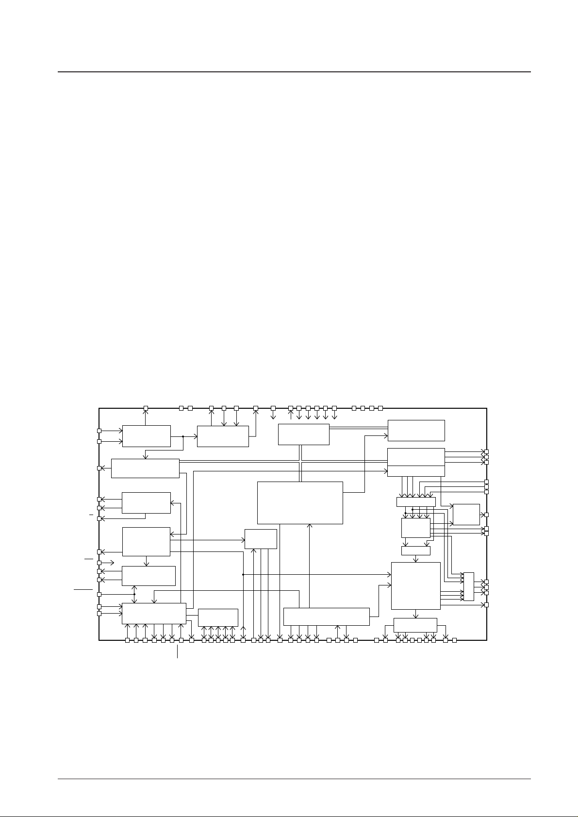
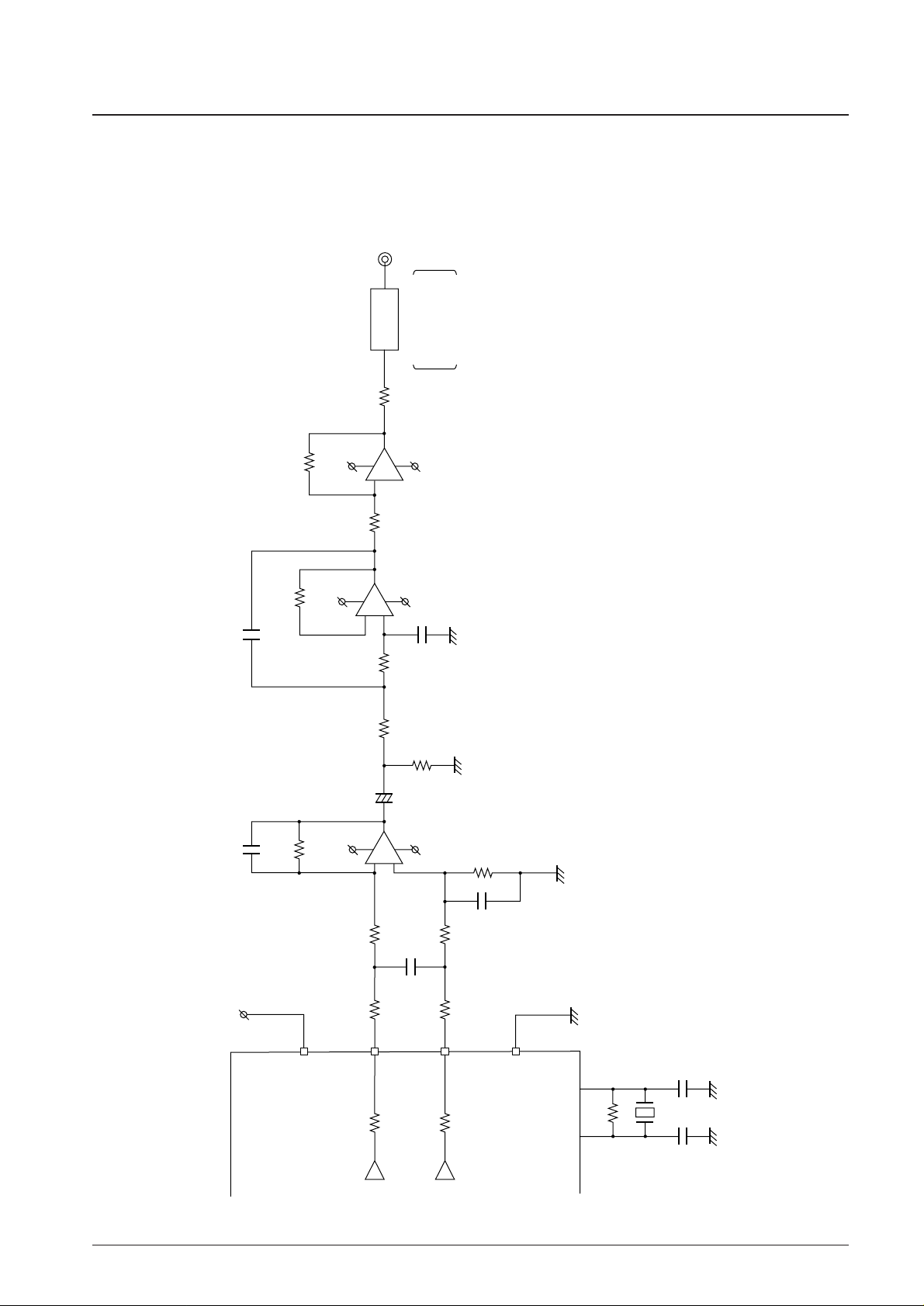
EFMO
VVDDVVSSPDO
ISETFRPCK
TAI
TST11
TEST1
TEST2
TEST3
TEST4
TEST5
VDDVSSV
DD
3V
V
SS
LRSY
C2F
ROMXA
LRCKI
BCKI
DATAI
DOUT
GAIN
HDCD
DFOLO
DACKO
LRCKO
DFORO
RWC
COIN
CQCK
SQOUT
WRQ
CS
TEST6
V/P
Slice level
control
Synchronization
EFM demodulation
CLV
digital servo
Subcode
separation
Q CRC
Microprocessor
interface
Servo
commander
I/O ports
Text
decoder
Crystal oscillator
System timing generator
1-bit DAC
MUX
M
U
X
HDCD
decoder
Interpolation
mute
2k × 8bits
RAM
C1 and C2 error
detection and correction
flag processing
VCO
clock control
RAM address
generator
Bilingual
MUX, S–P
Digital
output
8·Fs HDCD
interpolation
filter
De-emphasis
attenuator
CLV–
CLV+
FSEQ
EFMIN
DEFI
MUTEL
LV
DD
LCHN
LCHP
RV
SS
LV
SS
RCHP
MUTER
RV
DD
XVDDXOUT
XIN
XV
SS
FSX
CK2
4.2M
16M
EFLG
SRDT
DQSY
SCLK
EMPH
P4
P3
P2
P1
P0
TGL
RES
JP+
JP–
TOFF
TES
PCCL
HFL
RCHN
A12795
Block Diagram
Page 3
Pin Assignment
No. 6329-3/40
LC78628E
A12796
SQOUT
COIN
CQCK
RES
TST11
SCLK
DQSY
4.2M
LC78628E
SRDT
TEST5
CS
LRSY
CK2
ROMXA
C2F
TEST1
P2
P1
P0
GAIN
DACKO
DFOLO
DFORO
LRCKO
EMPH
TEST4
16M
JP–
JP+
VDD3V
TEST3
HDCD
40
39
38
37
36
35
34
33
32
31
30
29
28
27
26
25
65
66
67
68
69
70
71
72
73
74
75
76
77
78
79
80
RWC64
WRQ63
FSX62
BCKI61
TEST660
DATAI59
EFLG58
LRCKI57
DOUT56
MUTER55
RV
DD
54
RCHP53
RCHN52
RV
SS
51
LV
SS
50
LCHN49
LCHP48
LV
DD
47
MUTEL46
XV
SS
45
XOUT44
XIN43
XV
DD
42
P341
DEFI 1
TAI 2
PDO 3
VV
SS
4
ISET 5
VV
DD
6
FR 7
V
SS
8
V
SS
9
EFMO 10
EFMIN 11
TEST2 12
CLV+ 13
CLV– 14
V/P 15
V
DD
16
P4 17
PCCL 18
HFL 19
TES 20
PCK 21
FSEQ 22
TOFF 23
TGL 24
Parameter Symbol Conditions Ratings Unit
Maximum supply voltage
V
DD
max1 VDD, VVDD, XVDD, LVDD, RV
DD
VSS– 0.3 to VSS+ 6.0 V
V
DD
max2 VDD3V VSS– 0.3 to VSS+ 4.0 V
Input voltage
V
IN
5 max VSS– 0.3 to VDD1 + 0.3 V
V
IN
3 max VSS– 0.3 to VDD2 + 0.3 V
Output voltage
V
OUT
5 max VSS– 0.3 to VDD1 + 0.3 V
V
OUT
3 max VSS– 0.3 to VDD2 + 0.3 V
Allowable power dissipation Pd max 500 mW
Operating temperature Topr –20 to +75 °C
Storage temperature Tstg –40 to +125 °C
Specifications
Absolute Maximum Ratings at Ta = 25°C, VSS= 0 V
Parameter Symbol Conditions
Ratings
Unit
min typ max
Supply voltage
V
DD
1VDD, VVDD, XVDD, LVDD, RV
DD
4.5 5.0 5.5 V
V
DD
2VDD3V 3.0 3.3 3.6 V
V
IH
1
DEFI, COIN, RES, HFL, TES, RWC, CQCK, TAI, SCLK,
0.8 VDD1V
DD
1V
High-level input voltage
CS, PCCL, LRCKI, BCKI, DATAI
V
IH
2 P0 to P4, TEST1 to TEST5, EMPH 0.7 VDD1V
DD
1V
V
IH
3 EFMIN 0.6 VDD1V
DD
1V
V
IL
1
DEFI, COIN, RES, HFL, TES, RWC, CQCK, TAI, SCLK,
0 0.2 VDD1V
Low-level input voltage
CS, PCCL, LRCKI, BCKI, DATAI
V
IL
2 P0 to P4, TEST1 to TEST5, EMPH 0 0.3 VDD1V
V
IL
3 EFMIN 0 0.4 VDD1V
Allowable Operating Conditions at Ta = 25°C, VSS= 0 V
Continued on next page.
Page 4
No. 6329-4/40
LC78628E
Continued from preceding page.
Notes: The same voltage must be applied to all 5 V system power supply pins.
* When used in conjunction with an ASP that provides a command interface, the stricter ratings of the ASP shall be given priority.
Parameter Symbol Conditions
Ratings
Unit
min typ max
Input level
V
IN
1 EFMIN: Slice level control 1.0 Vp-p
V
IN
2 XIN: Capacitor coupled input 1.0 Vp-p
Data setup time t
SU
COIN, RWC, *: See figure 1. 400 ns
Data hold time t
HD
COIN, RWC, *: See figure 1. 400 ns
High-level clock pulse width t
WH
CQCK, *: See figures 1 and 2. 400 ns
Low-level clock pulse width t
WL
CQCK, *: See figures 1 and 2. 400 ns
Data read access time t
RAC
SQOUT: See figures 2. 0 400 ns
Command output time t
RWC
RWC, *: See figures 1. 1000 ns
Subcode Q readout enable time t
SQE
WRQ, normal speed: See figures 2, RWC = VIL1 11.2 ms
Port input setup time t
CSU
P0 to P4, RWC: See figures 3. 400 ns
Port input hold time t
CHD
P0 to P4, RWC: See figures 3. 400 ns
Port input clock setup time t
RCQ
CQCK, RWC, *: See figures 3. 100 ns
Port output data delay time t
CDD
P0 to P4, RWC: See figure 4. 1200 ns
Text readout period t
CW
DQSY, normal speed: See figure 5. 1.5 3.3 3.7 ms
DQSY pulse width t
W
DQSY, normal speed: See figure 5. 60 136 150 µs
SCLK high-level clock pulse width t
WTH
SCLK: See figure 5. 100 ns
SCLK low-level clock pulse width t
WTL
SCLK: See figure 5. 100 ns
SCLK clock delay time t
D
1 SCLK: See figure 5. 100 ns
Text data delay time
t
D
2 SRDT: See figure 5. 50 ns
t
D
3 SRDT: See figure 5. 50 ns
Reset time t
RES
RES 400 ns
Operating frequency range f
OP
EFMIN 10 MHz
Crystal oscillator frequency f
X
XIN, X
OUT
16.9344 MHz
Page 5
No. 6329-5/40
LC78628E
Parameter Symbol Conditions
Ratings
Unit
min typ max
Current drain
I
DD
1VDD, VVDD, XVDD, LVDD, RVDD: 4.5 V to 5.5 V 17 24 mA
I
DD
2VDD3V: 3.0 V to 3.6 V 55 85 mA
I
IH
1
DEFI, EFMIN, SCLK, COIN, RES, HFL, TES, RWC, –10 +10 µA
High-level input current
CQCK, TEST1, LRCKI, BCKI, DATAI, XIN: V
IN
= VDD1
I
IH
2 TAI, TEST2 to TEST5, CS, PCCL: VIN= VDD1 10 200 µA
DEFI, EFMIN, SCLK, COIN, RES, HFL, TES, RWC,
Low-level input current I
IL
CQCK, TAI, TEST1 to TEST5, CS, PCCL, LRCKI, BCKI, –10 +10 µA
DATAI, XIN: V
IN
= 0 V
V
OH
1 EFMO: IOH= –1 mA 4 V
CLV
+
, CLV–, V/P, P0 to P4, PCK, FSEQ, TOFF, TGL,
JP
+
, JP–, 16M, EMPH, LRCKO, DACKO, DFOLO,
V
OH
2 DFORO, GAIN, MUTEL, MUTER, DOUT, EFLG, TEST6, VDD1 – 2.1 V
High-level output voltage FSX, WRQ, SQOUT, TST11, DQSY, 4.2M, SRDT, LRSY,
CK2, ROMXA, C2F: I
OH
= –4 mA
V
OH
3 HDCD: IOH= –12 mA VDD1 – 2.1 V
V
OH
4 LCHP, LCHN, RCHP, RCHN: IOH= –1 mA 3.0 4.5 V
V
OL
1 EFMO: IOL= 1 mA 1V
CLV
+
, CLV–, V/P, P0 to P4, PCK, FSEQ, TOFF, TGL,
JP
+
, JP–, 16M, EMPH, LRCKO, DACKO, DFOLO,
Low-level output voltage
V
OL
2 DFORO, GAIN, MUTEL, MUTER, DOUT, EFLG, TEST6, 0.4 V
FSX, WRQ, SQOUT, TST11, DQSY, 4.2M, SRDT, LRSY,
CK2, ROMXA, C2F: I
OL
= 4 mA
V
OL
3 HDCD: IOL= 12 mA 0.4 V
V
OL
4 LCHP, LCHN, RCHP, RCHN: IOH= 1 mA 0.5 2.0 V
Output off leakage current I
OFF
1
PDO, CLV
+
, CLV–, JP+, JP–, P0 to P4, EMPH, SQOUT,
–10 +10 µA
EFMO: In the high-impedance output state
Charge pump output current
I
PDOH
PDO: R
ISET
= 68 kΩ 64 80 96 µA
I
PDOL
PDO: R
ISET
= 68 kΩ –96 –80 –64 µA
Electrical Characteristics at Ta = 25°C, VDD1 = 5 V, VDD2 = 3.3 V, VSS= 0 V
Page 6

No. 6329-6/40
LC78628E
Parameter Symbol Conditions
Ratings
Unit
min typ max
LCHP, LCHN, RCHP RCHN;
Total harmonic distortion THD + N 1 kHz: 0 dB data input 0.009 0.012 %
With the 20 kHz low-pass filter (internal AD725D) used.
LCHP, LCHN, RCHP, RCHN;
Dynamic range DR
1 kHz: –60 dB data input
83 86 dB
With the 20 kHz low-pass and A filters (internal AD725D)
used.
LCHP, LCHN, RCHP, RCHN;
Signal-to-noise ratio S/N
1 kHz: 0 dB data input
98 103 dB
With the 20 kHz low-pass and A filters (internal AD725D)
used.
LCHP, LCHN, RCHP, RCHN;
Crosstalk (separation) CT 1 kHz: 0 dB data input 96 98 dB
With the 20 kHz low-pass filter (internal AD725D) used.
D/A Converter Block Analog Characteristics at Ta = 25°C, VDD= LVDD= RVDD= XVDD= VVDD= 5 V,
VDD3V = 3.3 V, VSS= LVSS= RVSS= XVSS= VVSS= 0 V.
Figure 1 Command Input
COIN
CQCK
RWC
t
SU
t
SU
t
WL
t
WH
t
HD
t
HD
t
RWC
A12797
Figure 2 Subcode Q Output
t
WH
t
SQE
t
WH
t
WL
WRQ
CQCK
SQOUT
RWC
t
RAC
A12798
Note: Measured in the normal speed playback of the Sanyo 1-bit D/A converter reference circuit.
Page 7

CQCK
RWC
P0 to P4
HDCD
GAIN
SQOUT
4.2M
RWC
t
CDD
P0 to P4
t
RA
P0 P1 P2 P3 P4
HDCD GAIN
t
CHD
t
RCQ
t
CW
t
CSU
t
D2
t
D3
t
D1
t
WTL
t
W
DQSY
SCLK
SRDT
t
WTL
Flag
D0 D1 D2 D127
A12799
A12800
A12801
No. 6329-7/40
LC78628E
Figure 3 General-Purpose Port Input Timing
Figure 4 General-Purpose Port Output Timing
Figure 5 Text Data Output Timing
Page 8
Reference Circuit for the 1-Bit D/A Converter Output Block
No. 6329-8/40
LC78628E
+
–
+
–
+
–
+
LC78628E
LV
DD
(RV
DD
)
LV
SS
(RV
SS
)
XOUT
8pF
X'tal:16.9344MHz
8pF
XIN
1MΩ
1kΩ
1kΩ
8.2kΩ
R1
+5V
+10V
–10V
R2
R3
R4
C1
360pF
C6
1200pF
C3
100pF
8.2kΩ
6.2kΩ
24kΩ
R5
C2
C4 R9
R10
47µF
100pF C5 4700pF
6.2kΩ
1.5kΩ
R8
1.5kΩ
10kΩ
100kΩ
LPF
Internal AD725D
manufactured
by Shibasoku.
LCH
(RCH)
Analog output
R11
R13
R12
OP2
OP1
OP3
13kΩ
+10V
10kΩ
+10V
–10V
–10V
R6
24kΩ
R7
10kΩ
LCHP
(RCHP)
LCHN
(RCHN)
A12802
Page 9
No. 6329-9/40
LC78628E
Pin Functions
Pin No. Pin I/O Function
1 DEFI I Defect detection signal (DEF) input (Must be connected to 0 V if unused.)
2 TAI I Test input. A pull-down resistor is built in. This pin must be connected to 0 V.
3 PDO O External VCO control phase comparator output
4VV
SS
—
PLL-related pins
Internal VCO ground. This pin must be connected to 0 V.
5I
SET
AI PDO output current adjustment resistor connection
6VV
DD
— Internal VCO power supply. 5 V system
7 FR AI VCO frequency range adjustment resistor connection
8V
SS
— Ground. This pin must be connected to 0 V.
9V
SS
— Ground. This pin must be connected to 0 V.
10 EFMO O
Slice level control
EFM signal output
11 EFMIN I EFM signal input
12 TEST2 I Test input. A pull-down resistor is built in. This pin must be connected to 0 V.
13 CLV
+
O
Spindle control servo outputs. CLV
+
outputs a high level for accelerate, and CLV–outputs a high level for decelerate.
14 CLV
–
O
A command is provided to set these pins to three-state output.
15 V/P O
Automatic rough servo/phase control switching monitor output. A high level indicates rough servo and a low level indicates
phase control.
16 V
DD
— 5 V system power supply
17 P4 I/O
General-purpose I/O port. If unused, this port must either be set to input mode and connected to the 0 V level, or be set to
output mode and left open.
General-purpose I/O command identification. A pull-down resistor is built in.
18 PCCL I High: Only general-purpose I/O port commands can be used for control
Low: All commands can be used for control.
19 HFL I Track detection signal input. This is a Schmitt input.
20 TES I Tracking error signal input. This is a Schmitt input.
21 PCK O EFM data reproduction clock monitor output. Outputs 4.3218 MHz when the phase is locked.
Synchronizing signal output.
22 FSEQ O Outputs a high level if the synchronizing signal detected from the EFM signal and the internally generated synchronizing
signal match.
23 TOFF O Tracking off state output
24 TGL O Tracking gain switching output. A low level output raises the gain.
25 HDCD O HDCD identification output. High: An HDCD disc is being played, Low: A normal disc is being played.
26 TEST3 I Test input. A pull-down resistor is built in. This pin must be connected to 0 V.
27 V
DD
3V — 3 V system power supply
28 JP
+
O
Track jump outputs.
JP
+
:
A high level indicates either acceleration during a jump towards outer tracks, or deceleration during a jump towards inner tracks.
29 JP
–
O
JP
–
:
A high level indicates either acceleration during a jump towards inner tracks, or deceleration during a jump towards outer tracks.
A command is provided to set these pins to three-state output.
30 16M O 16.9344 MHz clock output
31 TEST4 I Test input. A pull-down resistor is built in. This pin must be connected to 0 V.
Deemphasis monitor output/input. A high level is output during playback of a deemphasis disc. When external data is applied
32 EMPH I/O to the HDCD filter engine, this pin is used for deemphasis switching. After a reset, this pin goes to monitor output mode in the
high-impedance state.
33 LRCKO O HDCD filter engine output word clock (8fs) or L/R clock output from the HDCD decoder (1fs).
34 DFORO O HDCD filter engine output right channel data (8fs)
35 DFOLO O HDCD filter engine output left channel data (8fs) or L/R data output from the HDCD decoder (1fs).
36 DACKO O HDCD filter engine output bit clock (8fs) or HDCD decoder output bit clock (1fs).
Analog output stage gain indicator
37 GAIN O
In internal gain scaling mode, this pin always outputs a high level (unused). Gain scaling is performed internally. Normal discs
are –6 dB. When external gain scaling is used, peak extend should be turned on when this pin is high, and should be turned
off when this output is low.
38 P0 I/O
General-purpose I/O port. If unused, this port must either be set to input mode and connected to the 0 V level, or be set to
output mode and left open.
39 P1 I/O
General-purpose I/O port. If unused, this port must either be set to input mode and connected to the 0 V level, or be set to
output mode and left open.
40 P2 I/O
General-purpose I/O port. If unused, this port must either be set to input mode and connected to the 0 V level, or be set to
output mode and left open.
41 P3 I/O
General-purpose I/O port. If unused, this port must either be set to input mode and connected to the 0 V level, or be set to
output mode and left open.
Continued on next page.
Page 10
No. 6329-10/40
LC78628E
Continued from preceding page.
Pin No. Pin I/O Function
42 XV
DD
— Crystal oscillator power supply. 5 V system.
43 X
IN
I
Connections for the 16.9344 crystal element and capacitors. Since no feedback resistor is built in, an external feedback
44 X
OUT
O
resistor must be provided.
45 XV
SS
— Crystal oscillator ground. This pin must be connected to 0 V.
46 MUTEL O Left channel audio data mute detection output
47 LV
DD
— Power supply. 5 V system.
48 LCHP O Left channel audio data P output
49 LCHN O Left channel audio data N output
50 LV
SS
—
Ground. This pin must be connected to 0 V.
51 RV
SS
— Ground. This pin must be connected to 0 V.
52 RCHN O Right channel audio data N output
53 RCHP O Right channel audio data P output
54 RV
DD
— Power supply. 5 V system.
55 MUTER O Right channel audio data mute detection output
56 DOUT O Digital output
57 LRCKI I Left/right clock input for external data input to the HDCD filter engine (1fs)
58 EFLG O C1/C2 single/double error correction monitor output
59 DATAI I Data input for external data input to the HDCD filter engine (20 bits)
60 TEST6 O Test output. Outputs the subcode frame sync signal. This pin must be left open when used.
61 BCKI I Bit clock input for external data input to the HDCD filter engine (48fs)
62 FSX O Outputs the 7.35 kHz sync detection signal divided from the crystal oscillator clock.
63 WRQ O Subcode Q output standby (ready) state output
64 RWC I Read/write control input. This is a Schmitt input.
65 SQOUT O Subcode Q output
66 COIN I Input for commands from the microcontroller
67 CQCK I Command input acquisition clock input, or clock input for readout of subcode data from SQOUT. This is a Schmitt input.
68 RES I IC reset input. Applications must apply a low level to this pin after power is first applied.
69 TST11 O Test output. This pin must be left open (it normally outputs a low level).
70 SCLK I Text data shift clock input
71 DQSY O Text data readout permission output
72 4.2M O 4.2336 MHz output
73 SRDT O Text data output
74 TEST5 I Test input. A pull-down resistor is built in. This pin must be connected to 0 V.
75 CS I Chip select input. A pull-down resistor is built in. (This pin must be connected to 0 V when not controlled.)
76 LRSY O Left/right clock output
77 CK2 O
ROMXA support outputs
Bit clock output (at reset) Polarity inverted clock output (in CK2CON mode)
78 ROMXA O Interpolated data output (at reset) ROM data output (in ROMXA mode)
79 CF2 O C2 flag output
80 TEST1 I Test input. There is no built-in pull-down resistor. This pin must be connected to 0 V.
Note: The equal power-supply voltage must be applied to all the 5 V system power supply pins.
Page 11
No. 6329-11/40
LC78628E
Internal Functions
1. HF signal input circuit — Pin 11: EFMIN, pin 10: EFMO, pin 1: DEFI, pin 13: CLV
+
When an HF signal is input to the EFMIN pin, an
EFM signal (NRZ) sliced at the optimal level is
acquired. As a measure to handle defects, when the
DEFI pin (pin 1) goes high, the slice level
controller output from the EFMO pin (pin 10) goes
to the high-impedance state, and the slice level is
held. However, this is only valid when the CLV
circuit is in phase control mode, that is, when the
V/P pin (pin 15) is outputting a low level.
This function can be implemented in combination
with the DEF pin from an LA9230/9240 series
product.
*: If the EFMIN and CLV+lines are run close
together, the error rate may increase due to
spurious radiation. We recommend inserting
either a ground or VDDshield line between these
lines.
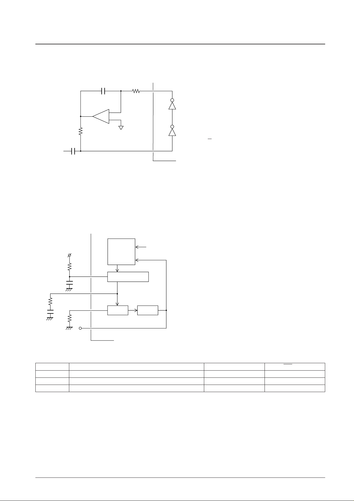
2. PLL clock regeneration circuit — Pin 3: PDO, pin 5: ISET, pin 7: FR, pin 21: PCK
The LC78628E includes a built-in VCO circuit,
and a PLL circuit is formed by adding external
resistors and capacitors. The ISET pin sets the
charge pump reference current, PDO sets the VCO
circuit loop filter, and FR sets the VCO frequency
range.
Sample values for reference purposes:
R1 = 68 kΩ, C1 = 0.1 µF
R2 = 680 Ω, C2 = 0.1 µF
R3 = 1.2 kΩ
+
–
SLC
SLI
VREF
1110EFMIN
EFMO
HF signal
A12803
V
DD
R1
C2
R2
R3
C1
5 ISET
EFM(NRZ)
PDO
FR
PCK
VCO 1/N
Charge pump
Frequency
and phase
comparator
3
21
7
A12804
Code Command Frequency divisor RES = low
$AC VCO × 2 SET 1
$AD VCO × 1 SET 2
$AE VCO × 0.5 SET 0.5
●●
The divisor used by the divider to create PCK from the VCO can be set using the VCO × 2, VCO ×1, and VCO × 0.5 SET instructions. Normally, the circuit
operates in the VCO × 0.5 SET state after a reset.
Page 12
3. VCO monitor — Pin 21: PCK
This pin monitors the 4.3218 MHz (on average) signal created by dividing the VCO frequency. In 2 × speed playback
mode, the frequency becomes 8.6436 MHz.
4. Sync detection monitor — Pin 22: FSEQ
When the frame sync (a positive sync signal) read from the EFM signal by PCK and the timing (interpolated sync
signal) generated with a counter match, this pin outputs a high level. Thus this pin functions as a sync detection
monitor. Note that it holds the high level for a single frame.
5. Servo command function — Pin 64: RWC, pin 66: COIN, pin 67: CQCK, pin 18: PCCL
The LC78628E instructions can be executed by setting RWC high and inputting the command to COIN in
synchronization with the CQCK clock. Note that the command is executed starting at the fall of the RWC signal.
Focus start
Track jump
Muting control - - - - - - One-byte commands
Disc motor control
Other control commands
Track check- - - - - - - - - - - - - - - - - - - - - - - - - - - - Two-byte command (RWC set twice)
General-purpose port I/O, E/D settings
Digital attenuator settings - - - - - - Two-byte commands (RWC set once)
HDCD control register settings
No. 6329-12/40
LC78628E
MSBLSB
MSB
LSB
Command ($F0, $F8) Data ($008 to $FE) or command ($FF)
MSB
LSB
RWC
CQCK
COIN
RWC
CQCK
COIN
A12805
A12806
• One-byte commands
• Two-byte command (RWC set twice)
Page 13

No. 6329-13/40
LC78628E
MSB
LSB
Data
Command ($81 to $87, $DB, $DC, $D8)
MSB
LSB
RWC
CQCK
COIN
A12807
• Two-byte commands (RWC set once)
Code Command RES = low
$FE Command input noise reduction mode
$EE Reset command input noise reduction mode ●●
This command reduces noise on the CQCK signal. Although this command is effective for noise pulses of less than 500 ns, the CQCK timing parameters tWL,
t
WH
, and tSUmust all be set to 1µs or longer.
• Command noise reduction
Code Command RES = low
$04 Disc motor start (accelerate)
$05 Disc motor CLV (CLV)
$06 Disc motor brake (decelerate)
$07 Disc motor stop (stop) ●●
The CLV+signal accelerates the disc in the forward direction, while the CLV–signal decelerates the disc. The corresponding mode, accelerate, decelerate,
CLV, or stop, is selected by the command sent from the microcontroller. The table below lists the CLV
+
and CLV–outputs in each of these modes.
6. CLV servo circuit — Pin 13: CLV+, pin 14: CLV–, pin 15: V/P
PCCL input level Command transfer during track check, track jump, and internal motor braking operations
L Incorrect operation occurs if a command is transferred (if a high level is applied to RWC).
H Transfer of only the port related ($DBXX and $DCXX) and HDCD register setting ($D8XX) commands is allowed.
Mode CLV
+
CLV
–
Accelerate H L
Decelerate L H
CLV Pulse output Pulse output
Stop L L
• PCCL
The PCCL control pin is provided to allow the use of certain commands for which command transfer is disabled during
track check, track jump, and internal motor braking operations.
A12808
1413CLV–
CLV+
+
–
+–
Disc motor
M
Note: The CLV servo control commands set the TOFF pin low during CLV mode, and high at all other times. The TOFF pin can only be controlled by
commands during CLV mode.
Page 14

• CLV mode
In CLV mode, the disc rotation is detected from the HF signal, and proper linear velocity rotation is achieved by
changing the DSP internal modes. The basic PWM period corresponds to a frequency of 7.35 kHz. The V/P pin outputs
a high level during rough servo operation and a low level during phase control.
No. 6329-14/40
LC78628E
Internal mode CLV
+
CLV
–
V/P
Rough servo (low-speed rotation recognized) H L H
Rough servo (high-speed rotation recognized) L H H
Phase control (PCK locked) PWM PWM L
Code Command RES = low
$A8 Disc 8 cm Set
$A9 Disc 12 cm Set ●●
The CLV control gain in rough servo mode can be set 8.5 dB lower for 8 cm discs that for 12 cm discs.
• Rough servo gain switching
Code Command RES = low
$B1 CLV phase comparator divided by 2
$B2 CLV phase comparator divided by 4
$B3 CLV phase comparator divided by 8
$B0 CLV No phase comparator division ●●
The phase control gain can be modified by switching the divisor provided by the divider circuit in the front end of the phase comparator.
• Phase control gain switching
13
CLV+
1/N
1/N
Phase
comparator
7.35 kHz
PCK/588
CLV–
14
A12809
CLV+
CLV+
CLV–
CLV–
Acceleration Deceleration
High-impedance output
3-value output
2-value output
A12810
Code Command RES = low
$B4 CLV 3-value output
$B5 CLV 2-value output (earlier technique) ●●
The CLV 3-value output command allows CLV control to be implemented using a single output pin. However, note that since the spindle gain is reduced by
6 dB, the servo side gain must be increased.
• CLV 3-value output
Page 15

No. 6329-15/40
LC78628E
Code Command RES = low
$C5 Internal braking: on
$C4 Internal braking: off ●●
$A3 Internal braking: control
$CB Internal braking continuous mode
$CA Reset continuous mode ●●
$CD Internal braking TON mode
$CC Reset TON mode ●●
• Issuing the internal braking on ($C5) command sets the LC78628E to internal brake mode. In this mode, the disc deceleration state can be monitored from
the WRQ pin when a brake command ($06) is executed.
• In this mode the disc deceleration state is determined by counting the EFM signal density in a single frame, and when the EFM signal count falls under four,
the CLV
–
pin is dropped to low. At the same time the WRQ signal, which functions as a brake completion monitor, goes high. When the microprocessor
detects a high level on the WRQ signal, it should issue a STOP command to fully stop the disc. In internal braking continuous mode, the CLV
–
pin highlevel output braking operation continues even after the WRQ brake completion monitor goes high. Note that if errors occur in deceleration state
determination due to noise in the EFM signal, the problem can be rectified by changing the EFM signal count from four to eight with the internal brake
control command ($A3).
• In internal braking TON mode ($CD), the TOFF pin is held low during internal braking operations. We recommend using this feature, since it is effective at
preventing incorrect detection at the disc mirror surface.
Notes: 1. If focus is lost during the execution of an internal brake command, the pickup must first be refocused and then the internal brake command must be
reissued.
2. Since incorrect state determination is possible depending on the EFM signal playback state (e.g., disc defects, access in progress), we recommend
using these functions in combination with a microprocessor.
• Internal brake modes
WRQ
CLV–
Disc motor
braking ($06)
EFM signal
CLV+
A12811
Code Command RES = low
$22 New track count mode (using the TES/HFL combination) ●●
$23 Previous track count mode (directly counts the TES signal)
The earlier track count function used the TES signal directly as the internal track counter clock.
To reduce counting errors resulting from noise on the rising and falling edges of the TES signal, the new track count function prevents noise induced errors
by using the combination of the TES and HFL signals, and implements a more reliable track count function. However, dirt and scratches on the disc can still
result in HFL signal dropouts that may result in missing track count pulses. Thus care is required when using this function.
7. Track jump — Pin 19: HFL, pin 20: TES, pin 23: TOFF, pin 24: TGL, pin 28: JP+, pin 29: JP
–
• Track counting types
The LC78628E supports the two track count modes listed below.
Page 16

No. 6329-16/40
LC78628E
Code Command RES = low
$A0 Previous Track Jump Mode ●●
$A1 New Track Jump Mode
$11 1 TRACK JUMP IN #1
$12 1 TRACK JUMP IN #2
$31 1 TRACK JUMP IN #3
$52 1 TRACK JUMP IN #4
$10 2 TRACK JUMP IN
$13 4 TRACK JUMP IN
$14 16 TRACK JUMP IN
$30 32 TRACK JUMP IN
$15 64 TRACK JUMP IN
$17 128 TRACK JUMP IN
$19 1 TRACK JUMP OUT #1
$1A 1 TRACK JUMP OUT #2
$39 1 TRACK JUMP OUT #3
$5A 1 TRACK JUMP OUT #4
$18 2 TRACK JUMP OUT
$1B 4 TRACK JUMP OUT
$1C 16 TRACK JUMP OUT
$38 32 TRACK JUMP OUT
$1D 64 TRACK JUMP OUT
$1F 128 TRACK JUMP OUT
$16 256 TRACK CHECK
$0F TOFF
$8F TON ●●
$8C TRACK JUMP BRAKE
$21 JP pulse period TOFF output mode
$20 Reset the JP pulse period TOFF output mode ●●
• Track jump commands
c
ba
JP–(+)
JP+(–)
(Braking period)
(JP pulse width)
TGL
A12812
When the LC78628E receives a track jump instruction as a servo command, it first generates accelerating pulses (period
a) and next generates deceleration pulses (period b). The passage of the braking period (period c) completes the specified
jump. During the braking period, the LC78628E detects the beam slip direction from the TES and HFL inputs. TOFF is
used to cut the components in the TES signal that aggravate slip. The jump destination track is captured by increasing the
servo gain with TGL. In JP pulse period TOFF output mode, TOFF goes high during the period that JP pulses are
generated.
Note: Of the modes related to disc motor control, the TOFF pin goes low only in CLV mode, and will be high during
start, stop, and brake operations. Note that the TOFF pin can be turned on and off independently by microprocessor
issued commands. However, this function is valid only when disc motor control is in CLV mode.
Page 17

No. 6329-17/40
LC78628E
• Track jump modes
The table lists the relationships between acceleration pulses (period a), deceleration pulses (period b), and the braking
period (period c).
Item
Previous track jump mode New track jump mode
abcabc
1 TRACK JUMP IN (OUT) #1 233 µs 233 µs 60 ms 233 µs 233 µs 60 ms
1 TRACK JUMP IN (OUT) #2
0.5 track
233 µs 60 ms
0.5 track The same time
60 ms
jump periods jump periods as a
1 TRACK JUMP IN (OUT) #3
0.5 track
233 µs
This period does 0.5 track The same time This period does
jump periods not exist. jump periods as a not exist.
1 TRACK JUMP IN (OUT) #4
0.5 track
233 µs
60 ms;
TOFF is low
0.5 track The same time 60 ms;
TOFF is low
jump periods
during the C period.
jump periods as a
during the C period.
2 TRACK JUMP IN (OUT) None
1 track The same time
60 ms
jump period as a
4 TRACK JUMP IN (OUT)
2 track
466 µs 60 ms
2 track The same time
60 ms
jump periods jump periods as a
16 TRACK JUMP IN (OUT)
9 track 7 track
60 ms
9 track The same time
60 ms
jump periods jump periods jump periods as a
32 TRACK JUMP IN (OUT)
18 track 14 track
60 ms
18 track 14 track
60 ms
jump periods jump periods jump periods jump periods
64 TRACK JUMP IN (OUT)
36 track 28 track
60 ms
36 track 28 track
60 ms
jump periods jump periods jump periods jump periods
128 TRACK JUMP IN (OUT)
72 track 56 track
60 ms
72 track 56 track
60 ms
jump periods jump periods jump periods jump periods
TOFF goes high during the period TOFF goes high during the period
256 TRACK JUMP IN (OUT)
when 256 tracks are passed over.
60 ms
when 256 tracks are passed over.
60 ms
The a and b period pulses are not The a and b period pulses are not
output. output.
TRACK JUMP BRAKE There are no a and b periods. 60 ms There are no a and b periods. 60 ms
Notes: 1. As indicated in the table, actuator signals are not output during the 256 TRACK CHECK function. This is a mode in which the TES signal is counted
in the tracking loop off state. Therefore, feed motor forwarding is required.
2. The servo command register is automatically reset after one cycle of the track jump sequence (a, b, c) completes.
3. If another track jump command is issued during a track jump operation, the track jump operation is immediately interrupted. Therefore, applications
must not issue a new command during a jump operation. However, port related commands and the HDCD register setting command can be used
by setting the PCCL pin.
4. The 1 TRACK JUMP #3 mode does not have a braking period (the C period). Since brake mode must be generated by an external circuit, care is
required when using this mode.
5. Although there was no braking period (period c) for the 2 TRACK JUMP IN/OUT new track jump mode in the LC78620/21/25 products, in this IC
(the LC78628E) the braking period for this mode has been modified to be 60 ms.
Page 18

No. 6329-18/40
LC78628E
A12813
+
–
HFL
19
24
TGL
23
TOFF
29
JP–
28
T.Coil
JP+
20
Slip detection
High during the braking period
TES
T.E.
(THLD)
TES (when moving out)
TES (when moving in)
HFL
TOFF output
A12814
JP+
JP+
JP–
JP–
Two-value output
Three-value output
High-impedance output
A12815
The THLD signal is generated by the LA9230/40 and the tracking error signal is held during the JP pulse period.
* Tracking brake
• The figure shows the relationships between the TES, HFL, and TOFF signals during the track jump c period. The
TOFF signal is extracted from the HFL signal by TES signal edges. When the HFL signal is high, the pickup is over
the mirror surface, and when low, the pickup is over pits region. Thus braking is applied based on the TOFF signal
being high when the pickup is moving from a mirror region to a pits region and on TOFF being low when the pickup
is moving from a data region to a mirror region in the increased gain state (TGL = low).
Code Command RES = low
$B6 JP three-value output
$B7 JP two-value output (earlier technique) ●●
The JP three value output command allows the track jump operation to be controlled from a single pin. However, the spindle gain is 6 dB lower when this pin
is used, so applications must increase the gain in the servo system.
• JP three-value output
Page 19

No. 6329-19/40
LC78628E
Code Command RES = low
$F0 Track check in
$F8 Track check out
$FF Two-byte command reset ●●
The LC78628E will count exactly one more than the specified number of tracks when the microprocessor sends an arbitrary binary value in the range 8 to
254 after issuing either a track check in or a track check out command.
Notes: 1. When the desired track count has been input in binary, the track check operation is started by the fall of RWC.
2. During a track check operation the TOFF pin goes high and the tracking loop is turned off. Therefore, feed motor forwarding is required.
3. When a track check in/out command is issued the function of the WRQ signal switches from the normal mode subcode Q standby monitor function
to the track check monitor function. This signal goes high when the track check is half completed, and goes low when the check finishes. The
control microprocessor should monitor this signal for a low level to determine when the track check completes.
4. If a two-byte reset command is not issued, the track check operation will repeat. That is, to skip over 20,000 tracks, issue a track check 199
command once, and then count the WRQ signal 100 times. This will check 20,000 tracks.
5. After performing a track check operation, use the brake command to have the pickup lock onto the track.
8. Error flag output — Pin 58: EFLG, pin 62: FSX
The FSX signal is a 7.35 kHz frame sync signal generated by dividing the crystal oscillator clock. The error correction
state for each frame is output from EFLG. While FSX is low, EFLG indicates the C1 correction and while FSX is high it
indicates the C2 correction. The playback OK/NG state can be easily determined from the number of high level pulses
that appear here.
The FSX and EFLG pins can be held at the low level by applying an FSX, TEST6, EFLG, LO command ($0A).
Applying an FSX, TEST6, EFLG, EN command ($0B) returns the IC to the original output mode.
• Track check mode
Two-byte command reset
($FF)
Falls to low when the track
check completes.
Rises at 1/2 the specified
track count
Input of the desired
number of tracks
minus 1 in binary
Track check in/out
command
($F0 or $F8)
RWC
WRQ
Track count
Command
Brake command
($8C)
A12816
C1
Single
correction
Double
correction
Correction
not possible
No errors
EFLG
FSX
C2
A12817
Page 20

No. 6329-20/40
LC78628E
Code Command RES = low
$09 ADDRESS FREE
$89 ADRESS = low ●●
Subcode Q can be read from the SQOUT pin by applying a clock to the CQCK pin.
Of the eight bits in the subcode, the Q signal is used for song (track) access and display. WRQ will be high only if the data passed the CRC error check and
the subcode Q format internal address is 1 *. The control microprocessor can read out data from SQOUT in the order shown below by detecting this high
level and applying CQCK. When CQCK is applied the DSP disables register update internally. The microprocessor gives update permission by setting RWC
high briefly after reading has completed. This causes WRQ to fall to low at this time. Since WRQ falls to low 11.2 ms after going high, CQCK must be applied
during the WRQ high period. Note that data is read out LSB first.
Note: * These conditions will be ignored if an address free command is sent. This is provided to handle CD-ROM applications.
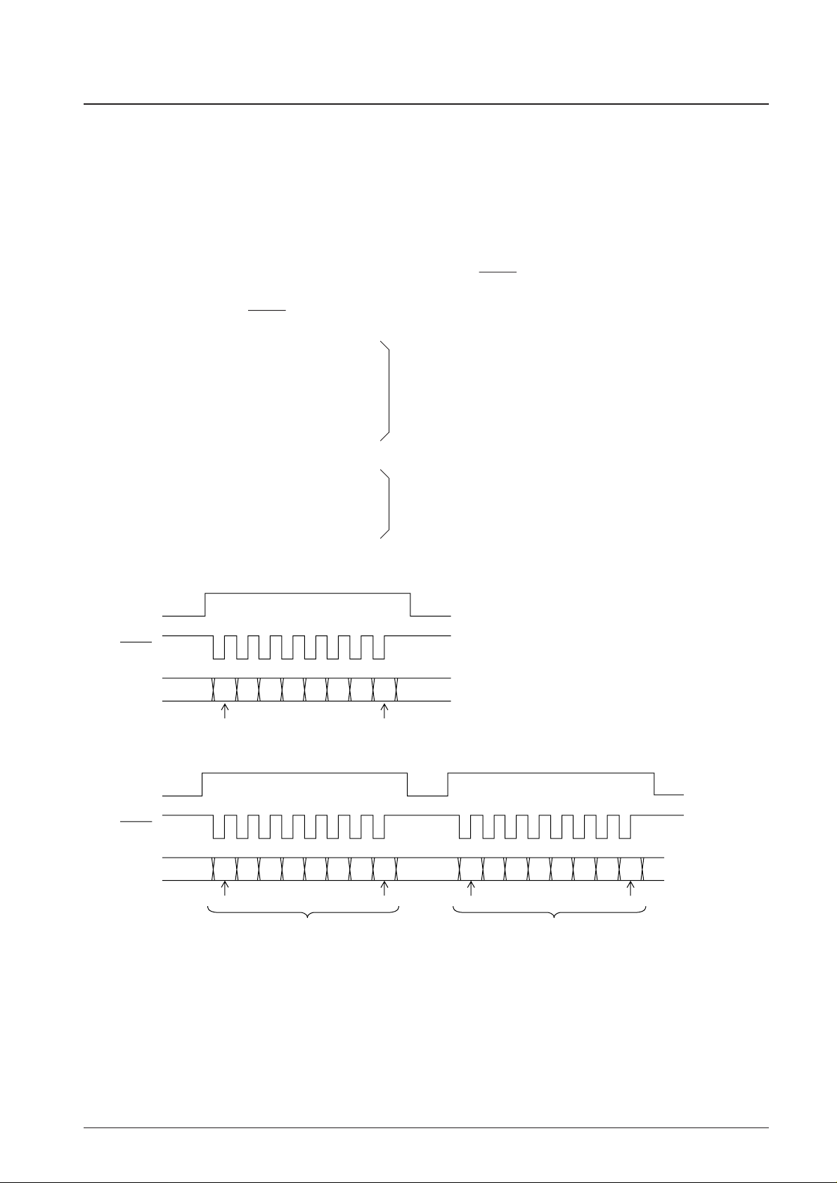
9. Subcode Q output circuit — Pin 63: WRQ, pin 64: RWC, pin 65: SQOUT, pin 67: CQCK, pin 75: CS
ADR CONT AFRAME
80 bits
WRQ
CQCK
SQOUT
RWC
SUBQ data
A12818
CONT
TNO
INDEX (POINT)
MIN
SEC Note: Items in parentheses
refer to the read-in area.
FRAME
ZERO
AMIN (PMIN)
ASEC (PSEC)
AFRAME (PFRAME)
ADR
8 bits
Notes: 1. Normally, the WRQ pin indicates the subcode Q standby state. However, it is used for a different monitoring purpose in track check mode and
during internal braking. (See the items on track counting and internal braking for details.)
2. The LC78628E becomes active when the CS pin is low, and subcode Q data is output from the SQOUT pin. When the CS pin is high, the SQOUT
pin goes to the high-impedance state.
Page 21

10. Text circuit
The text function decodes and outputs the song titles and other text data written to the subcode R through W channels
in the compact disc read entry area.
A single pack, which is the subcode R through W data for 24 symbols (18 bytes = 144 (24 × 6 = 18 × 8) bits),
consists of 4 bytes of ID data, 12 bytes of text data, and 2 bytes of CRC data. The data that can be read out from the
LC78628E consists of a result flag for the CRC check (1 bit) and the 16 bytes of the ID and text data. When the IC is
in a state where the data can be read out, it outputs a low-level pulse (minimum: 60 µs, maximum: 150 µs) from the
DQSY pin and outputs, from the SRDT pin, the CRC check result flag (OK: high, NG: low) for the one pack of data
that can be read out. After the control microprocessor detects the low level on the DQSY pin, it can read out the data
serially from the SRDT by applying 128 transfer clock pulses to the SCLK pin. The application must complete the
readout of one pack of data within 3.3 ms in normal-speed playback mode, and within 1.5 ms in 2 × -speed playback
mode. Since the type and other information concerning the following text data is encoded in the ID data, the control
microprocessor must interpret the text data according to the ID data.
No. 6329-21/40
LC78628E
Data for one pack
1 packet = 4 packs
SBSY
DQSY
SCLK
SRDT
DQSY
SCLK
SRDT
CRC D0 D1 D2 D3 D4 D5 D6 D127 D0 D1 D2 D3 D4 D5
D126
••••••••••••••••••••••••••••••••••••
CRC
•••••••••
A12819
: Correct data
: Flagged data
: Linearly interpolated data
: Data converging
to the mute level
A12820
Code Command RES = low
$01 MUTE 0 dB
$02 MUTE –12 dB
$03 MUTE –∞ dB ●●
An attenuation of 12 dB (MUTE –12 dB) or full muting (MUTE –∞ dB) can be applied by issuing the appropriate command from the table. Since zero cross
muting is used, there is minimal noise associated with this function. Zero cross is defined for this function as the top seven bits being all ones or all zeros.
Caution: Note that it may become impossible to detect HDCD discs if either the $02 or $03 instruction is executed.
11. Muting control circuit
12. Interpolation circuit
The output of incorrect audio data that could not be corrected by the error detection and correction circuit would
result in loud noise in the output. To minimize this noise, the LC78628E replaces the incorrect data with linearly
interpolated data based on the correct data on either side of the incorrect data. More precisely, the LC78628E uses
this technique if C2 flags occurred up to three times in a row. If C2 flags occurred four or more times in a row, the
LC78628E converges the output level to the muting level. However, when correct data is finally output following
four or more C2 flag occurrences, the LC78628E replaces the 3 data items between the data actually output at the
fourth preceding item and the correct data with data linearly interpolated between those two values.
Page 22

No. 6329-22/40
LC78628E
Code Command RES = low
$28 STO CONT ●●
$29 Lch CONT
$2A Rch CONT
• Following a reset or when a stereo ($28) command has been issued, the left and right channel data is output to the left and right channels respectively.
• When an Lch set ($29) command is issued, the left and right channels both output the left channel data.
• When an Rch set ($2A) command is issued, the left and right channels both output the right channel data.
• This function applies to the 16-bit data output to the HDCD decoder and ROMXA pin. This means that it may become impossible to recognize HDCD discs
when either the Lch CONT or Rch CONT mode in this function has been set up.
13. Bilingual function
Code Command RES = low
$88 CD-ROMXA
$8B CD-ROM XA reset ●●
$C9 CK2 polarity inversion
14. CD-ROM outputs — Pin 76: LRSY, pin 77: CK2, pin 78: ROMXA, pin 79: C2F
Although the LC78628E is initially set up to output audio data from the interpolation circuit MSB first from the
ROMXA pin in synchronization with the LRSY signal, it can be switched to output CD-ROM data by issuing a CDROMXA command. Since this data has not been processed by the interpolation, muting, and other digital circuits, it
is appropriate for input to a CD-ROM encoder IC. CK2 is a 2.1168 MHz clock, and data is output on the CK2 falling
edge. However, this clock polarity can be inverted by issuing a CK2 polarity inversion command. C2F is the flag
information for the data in 8-bit units.
SPDHDCD ROMXA Data output from the DOUT pin RES = low
0 0 16-bit audio data after interpolation and muting processing ●●
0 1 16-bit data before interpolation and muting processing
10
20-bit audio data following HDCD processing.
11
15. Digital output circuit — Pin 56: DOUT
This output pin is provided for use with a digital audio interface. Data is output in the EIAJ format. The data output
from DOUT can be switched as listed below by the ROMXA flag set by the CD-ROMXA ($88) or CD-ROMXA
reset ($8B) commands and by the SPDHDCD flag in the HDCD control register.
CK2 positive
polarity mode
CK2 inverted
polarity mode
LRSY
ROMXA
0 “0” “0”
151413121110 9 8 7 6 5 4 3 2 1 0 151413121110 9 8 7 6 5 4 3 2 1 0
214847464544434241403938373635343332312625242322212019181716151413121110983214847
214847464544434241403938373635343332312625242322212019181716151413121110983214847
LSB
LRSY = 44.1 kHz (N times disc speed)
CK2 = 2.1168 MHz (N times disc speed)
Rch
MSBLSB
Lch
LSB C2 flags MSB C2 flags LSB C2 flagsMSB C2 flags
MSB
C2F
A12821
Page 23

No. 6329-23/40
LC78628E
Code Command Function RES = low
$42 DOUT ON Enabled state for output of the various data types from DOUT. ●●
$43 DOUT OFF Sets the DOUT output to be fixed at the low level.
$40 UBIT ON Of the DOUT data, the subcodes Q through W are output as the UBIT information. ●●
$41 UBIT OFF Of the DOUT data, the UBIT information is set to all zeros.
$88 CDROM-XA The ROMXA flag is set to 1.
$8B ROMXZ-RST The ROMXA flag is set to 0. ●●
The following table lists the DOUT related commands. See the item on the HDCD control register for details on the
method for setting the SPDHDCD flag.
16. One-bit D/A converter — Pin 48: LCHP, pin 49: LCHN, pin 52: RCHN, pin 53: RCHP, pin 46: MUTEL,
pin 55: MUTER
The LC78628E PWM block outputs a single data value in the range –3 to +3 once every 64 fs period. To reduce
carrier noise, this block adopts an output format in which each data switching block is adjusted so that the PWM
output level does not invert. This block outputs a positive phase signal to the LCHP (RCHP) pin and a reverse phase
signal to the LCHN (RCHN) pin. High-quality analog signals can be acquired by taking the differences of these two
output pairs using external low-pass filters. Note that the LC78628E includes built-in radiation suppression resistors
(1 kΩ) in each of the LCHP/N and RCHP/N pins.
Additionally, if the played back song data (source signal) goes to zero continuously for longer than a certain fixed
period (about 100 ms in normal-speed playback), the IC goes to D/A converter muting mode and outputs zero-valued
data (a 50/50 duty). Since this zero detection function operates independently for the left and right channels, when
zero is detected and muting mode is turned on, a high level is output from either the MUTEL or MUTER pin,
according to the channel in which zero was detected.
PWM output format
–3
+3)
–2
+2
–1
+1
0
0
+1
–1
+2
–2
+3
(–3
LCHP
(RCHP)
One data item
2.8224 MHz(64 fs)
LCHN
(RCHN)
+3
–3)
+2
–2
+1
–1
0
0
–1
+1
–2
+2
–3
(+3
–2–3+3 +1+1–10+2
Data value
LCHP
(RCHP)
LCHN
(RCHN)
A12823
A12822
PWM output example
Page 24

No. 6329-24/40
LC78628E
XDSEL Zero detection D/A converter muting circuit source signal RES = low
0 16-bit data read from the disc ●●
1 Data input from the LRCKI, BCKI, and DATAI pins
The source signal for the zero detection D/A converter muting circuit can be switched as shown below by the XDSEL
flag in the HDCD control register.
17. HDCD function
• Detailed block diagram of the HDCD function area
• HDCD block functions
— Automatic discrimination of HDCD encoded discs
— PE, GS, and LLE processing (HDCD decoder block)
— HDCD and GAIN signal output
—8 × oversampling HDCD filters, deemphasis, and attenuation (HDCD filter block)
— Output of HDCD decoded signals to the digital interface block
— Output of HDCD decoded signals to LRCKO, DACKO, and DFOLO
— Output of HDCD filtered signals from LRCKO, DACKO, DFOLO, and DFORO
— Output of HDCD filtered signals to the D/A converter block
— HDCD filter block source signal switching
When data with value other than zero is input as a source signal, the mute detection circuit immediately turns off and
the MUTEL or MUTER pin returns to the low level.
EMPH
LRCKI,BCKI,DATAI
MUTER
MUTEL
GAIN
HDCD
RCHP
RCHN
LCHN
LCHP
DAC
HDCD decoder
NS,
PWM
Zero
detection
muting
HDCD filter
attenuator,
8 fs HDCD
Interpolation
filter,
De-emphasis
LRCKO
DACKO
DFOLO
DFORO
DOUT
Digital output
interface
M
U
X
M
U
X
M
U
X
M
U
X
M
U
X
M
U
X
HDCD
detection
Deemphasis
control signal
Interpolation
and
muting
HDCD
control
register
PE,
LLE,
GS
PE: Peak extension
LLE: Low-level extension
GS: Gain scaling
A12824
Page 25

Peak Extension (PE)
HDCD includes a function called peak extension. Peak extension is an optional function that applies a digitally
implemented soft limit (6 dB) to rare peaks in the music signal before recording on the disc. HDCD discs include ones to
which peak extension has been applied, and ones to which peak extension has not been applied. The LC78628E HDCD
decoder block automatically detects this optional peak extension processing and restores the attenuated peaks to their
original shape.
Gain Scaling (GS)
After decoding, recordings to which peak extension was applied have peaks that are 6 dB higher, and the D/A converter
must reproduce these peaks. Therefore, the D/A converter input block average level is reduced by 6 dB. This average
level must be matched to the average level when recordings made without peak extension or non-HDCD recordings are
played back. This average level adjustment is called gain scaling (GS).
The LC78628E allows applications to switch between performing this gain scaling digitally within the IC or externally
using analog circuits. The EXSCA flag in the HDCD control register is used for this setting. The GAIN pin is used as the
control signal if gain scaling is performed in the analog domain.
Low-Level Extension (LLE)
HDCD includes a function called low-level extension. This is a function that compares the average level of a song to a
threshold level and raises that average level (i.e., it compresses the low levels). This is an optional function, and there are
both HDCD recordings that are made with low-level extension, and ones in which it is not used. The LC78628E
automatically recognizes low-level extension discs and returns compressed low levels to their original values.
HDCD Signal Output — Pin 25: HDCD
If the disc being played back was HDCD encoded, the HDCD output pin outputs a high level. At all other times it outputs
a low level. This pin output can be used in end products to provide an LED indicator that indicates when an HDCD disc
is being played. The HDCD signal can also be read by the control microprocessor using the port input instruction.
Gain Signal Output — Pin 37: GAIN
The GAIN pin is used when gain scaling is performed in the analog domain. This pin must be left open if gain scaling is
performed in the digital domain.
When analog gain scaling is used, a high level is output from the GAIN pin to indicate that peak extension processing
had been applied to the disc being played back. A low level is output from the GAIN pin for HDCD discs that did not
have peak extension applied and for non-HDCD discs. For analog domain gain scaling, the application must include an
external circuit that, when the GAIN pin output level is high, increases the output level by 6 dB over the level when the
pin output level is low. The GAIN signal can also be read out using the port input instruction.
Digital Attenuator
The HDCD filter block includes a digital attenuator that allows the attenuation level to be set in 0.5 dB steps with
commands. After a reset, the attenuation level goes to fully muted (the –∞ muted state with an attenuation code of $00).
This means that applications must set the attenuation code to $FF (the maximum setting value) to output the audio signal.
The attenuation code can be set to one of 256 values from $00 to $FF (0.5 dB steps) by applying commands from the
control microprocessor. The setting command is a 2-byte command. This command differs from the 2-byte command
used for track checking, and is the type where 16 bits of command data are transferred consecutively after setting RWC
high. There is no need to send the 2-byte command reset instruction ($FF) after using this command. (See the “Two-byte
commands (RWC set once)” section on page 13.)
No. 6329-25/40
LC78628E
EXSCA Gain scaling type RES = low
0 Digital gain scaling ●●
1 Analog gain scaling
Page 26

No. 6329-26/40
LC78628E
Code Command RES = low
$81xx ATT DIRECT SET DATA $00 SET (ATT –∞dB)
$82xx ATT 4-STEP UP
$83xx ATT 4-STEP DOWN
$84xx ATT 8-STEP UP
$85xx ATT 8-STEP DOWN
$86xx ATT 16-STEP UP
$87xx ATT 16-STEP DOWN
The attenuator STEP UP/DOWN commands ($82xx to $87xx) can be used to gradually change the attenuation level to
the target value in one code step (0.5 dB) at a time every 4, 8, or 16 samples. The target value can be loaded directly by
using the attenuator DIRECT SET command ($81xx).
When the attenuator STEP UP command is used, the target attenuation code must have a larger value than the code set at
that point. When the attenuator STEP DOWN command is used, inversely, the target attenuation code must have a
smaller value than the code set at that point. Also note that when either the attenuator STEP UP or DOWN command is
issued, the next attenuator setting command must not be issued until the preceding STEP UP/DOWN command has
completed, i.e. the circuit has reached the target value.
The following formula can be used to estimate the time required for the attenuation value to reach the target value set by
an attenuator STEP UP/DOWN command.
(target code – current code) × (4, 8, or 16)
———————————————————— [ms]
44.1 kHz (normal speed) or 88.2 kHz (2 × speed)
The attenuator can be set in 0.5 dB steps, and the amount of attenuation can be calculated from the following formula.
attenuation = (data value – 255) × 0.5 [dB]
Note that since this digital attenuator is located after the HDCD detection circuit, it will not affect HDCD discrimination,
no matter what attenuation level is set.
8 × Oversampling HDCD Interpolation Filters
The 20-bit 1 fs data processed in the HDCD decoder block is 8 × oversampled by the 8 × oversampling HDCD
interpolation filters in the HDCD filter block. However, 4 × oversampling is used in double-speed playback.
RWC
Command
LSB MSB
Attenuator setting commandAttenuation code
A12825
LR
Internal fs signal
Four steps down
ATT DATA
Start Stop
44.1 kHz (normal speed), 88.2 kHz (2 × speed)
A12826
Page 27

No. 6329-27/40
LC78628E
Deemphasis Filter — Pin 32: EMPH
The HDCD filter block includes a built-in deemphasis filter so that music that is recorded with preemphasis applied can
be played back with deemphasis. The HDCD filter block can operate with its input taken from either the audio signal
read from a disc or from the audio signal input to the LRCKI, BCKI, and DATAI pins.
The EMPH pin in an I/O pin that provides two functions:
• Monitor output for the preemphasis on/off bit for the audio signal being read out from the disc.
• Input for a signal that controls deemphasis on/off for the audio signal input to the pins.
These functions are switched by the XDSEL and EMPHOEN flags in the HDCD control register as listed below.
HDCD Decoded Signal Output to the Digital Interface Block
The 20-bit data processed by the HDCD decoder can be output as digital data from the DOUT pin. The average level of
the output data will differ depending on the digital/analog setting for the gain scaling mode and the type of the disc being
played back. The values shown in the table are levels relative to the average value of the source signal.
HDCD Decoded Signal Output from LRCKO, DACKO, DFOLO, and DFORO — Pin 33: LRCKO, pin 36: DACKO,
pin 35: DFOLO, pin 34: DFORO
HDCD decoded 1fs 20-bit data can be output digitally from the LRCKO, DACKO, DFOLO, and DFORO pins. The
output data is identical to that output from the DOUT pin.
It is also possible to output post-HDCD decoder processing HDCD processed 8 × oversampled 20-bit data (or 4 ×
oversampled 20-bit data in double-speed mode) from the LRCKO, DACKO, DFOLO, and DFORO pins. This 8 ×
oversampled signal has had internal deemphasis filtering and attenuator processing applied.
The 1FSOUT flag in the HDCD control register is used to switch between the above two types of data output.
The 16-bit data read out from the disc can also be output from the DOUT pin. That switching is controlled by the
SPDHDCD flag in the HDCD control register.
EMPOEN XDSEL EMPH pin state Deemphasis filter control signal source RES = low
0 0 Must be tied either high or low.
The subcode Q preemphasis on/off information
●●
High: on, low: off.
01
The deemphasis on/off signal must be applied. The signal applied to the EMH pin
High: on, low: off. High: on, low: off.
10
Outputs the subcode Q preemphasis on/off information The subcode Q preemphasis on/off information
High: on, low: off. High: on, low: off.
1 1 Do not set this mode. The IC may operate incorrectly.
GS mode Digital scaling Analog scaling
Disc type (EXSCA = 0) (EXSCA = 1)
PE processed HDCD disc –6 dB
When GAIN is low: 0 dB
When GAIN is high: –6 dB
HDCD disc that was not PE processed –6 dB 0 dB
Non-HDCD disc –6 dB 0 dB
SPDHDCD Data output from the DOUT pin RES = low
0 Pre-HDCD decoder processing 1 fs 16-bit data ●●
1 Post-HDCD decoder processing 1 fs 20-bit data
1FSOUT Data output from LRCKO, DACKO, DFOLO, and DFORO RES = low
0 Post-HDCD filter processing 8 fs data ●●
1 Pre-HDCD filter processing 1 fs data
Page 28

No. 6329-28/40
LC78628E
XDSEL DIN16 Input source signal to the HDCD filter block RES = low
00
HDCD decoder block 20-bit output data
●●
01
1 0 20-bit data input to the LRCKI, BCKI, DATAI, and EMPH pins
1 1 16-bit data input to the LRCKI, BCKI, DATAI, and EMPH pins
• Timing when 1FSOUT is 0
• Timing when 1FSOUT is 1
HDCD Filter Processed Signal Output to the D/A Converter Block
The 8 × oversampled data (4 × oversampled in double-speed playback) processed by the HDCD filter block is transferred
to the internal D/A converter block, converted to PWM data, and output from the LCHP, LCHN, RCHN, and RCHP pins.
This 8 × oversampling filter output signal has had internal deemphasis filtering and attenuator processing applied.
HDCD Filter Block Source Switching — Pin 57: LRCKI, pin 61: BCKI, pin 59: DATAI, pins 32: EMPH
The signal to be processed in the HDCD filter block can be set to be either the 20-bit data from the HDCD decoder block
or external data with the XDSETL flag in the HDCD control register. If data input from outside the IC is selected as the
HDCD filter block source signal, the bit length of that data (i.e. the serial input format) can be switched as shown in the
table below using the DIN16 flag in the HDCD control register.
LRCKO
LSB
DFOLO
DFORO
DACKO
2 1
LSB
2 1
LRCKO
LSB MSB
DFOLO
1716151413121110 9 8 7 6 5 4 3 2 1
18
1/352.8 kHz
MSB
18 17 16 15 14 13 12 11 10 9 8 7 6 5 4 3 2 1
MSB
181716151413121110987654321
Normal speed: 1/44.1 kHz, 2 × speed: 1/88.2 kHz
LSB
MSB
18171615 1314 121110 9 8 7 6 5 4 3 2 1
LSB
LSB
MSB
MSB
A12827
LSB
DFORO
DACKO
Lch
Rch
A12828
Page 29

No. 6329-29/40
LC78628E
Normal speed: 1/44.1 kHz, 2 × speed: 1/88.2 kHz
Rch
18
LSB MSB
1716151413121110 9 8 7 6 5 4 3 2 1
LSB
MSB
18171615 1314 121110 9 8 7 6 5 4 3 2 1
LSB
Lch
DATAI
LRCKI
BCKI
A12829
Normal speed: 1/44.1 kHz, 2 × speed: 1/88.2 kHz
Rch
LSB
151413121110 9 8 7 6 5 4 3 2 1
LSB
MSB
1314 121110 9 8 7 6 5 4 3 2 1
LSB
Lch
DATAI
LRCKI
BCKI
A12830
01234567COIN
CQCK
RWC
A12831
• Timing when 20-bit data is input to IC pins
• Timing when 16-bit data is input to IC pins
• Use 20-bit input mode when inputting, to the LRCKI, BCKI, and DATAI pins, post-HDCD decoding 20-bit data that
was recorded on MD and using this IC’s internal D/A converter for playback.
• When the HDCD filter block input source is set to pin input by setting XDSEL flag to 1, do not set the IC to CD
playback state. In this case, if gain scaling is set to analog gain scaling mode, the GAIN pin will output a low level,
and if set to digital gain scaling mode, it will output a high level.
• Clocks applied to the LRCKI and BCKI pins must be synchronized with the LC78628E’s system clock.
HDCD Control Register (CRHDCD)
The HDCD control register consists of 6 flags used for setting the modes associated with HDCD operations. This section
presents the method for setting this register and the meanings of the flags.
• Setting procedure
The HDCD control register is set using the following 2-byte command.
Instruction code: $D8xx (2-byte command)
Here, xx corresponds to the flags in CRHDCD, and bits transferred as a high level are set to 1.
Page 30

No. 6329-30/40
LC78628E
• Flag bit allocation in the register
Flag Function After a reset
EXSCA
0 The 6 dB gain scaling operation is performed internally. ●●
(bit 0)
1 The 6 dB gain scaling operation is performed externally. The GAIN output pin is used.
XDSEL
0 Data from the HDCD decoder block is applied to the HDCD filter block. ●●
(bit 1)
1 Data input from the LRCKI, BCKI, and DATAI pins is applied to the HDCD filter block.
1FSOUT
0 Data from the HDCD filter block is output from the LRCKO, DACKO, DFOLO, and DFORO pins. (8 fs) ●●
(bit 2)
1 Data from the HDCD decoder block is output from the LRCKO, DACKO, DFOLO, and DFORO pins. (1 fs)
Reserved
— This flag must always be set to 0. —
(bit 3)
SPDHDCD
0 Pre-HDCD processing 16-bit data read out from the disc is output from the DOUT pin. ●●
(bit 4)
1 The 20-bit data from the HDCD decode block is output from the DOUT pin.
Reserved
— This flag must always be set to 0. —
(bit 5)
DIN16
0 The data input to the DATAI pin has a bit length of 20 bits. ●●
(bit 6)
1 The data input to the DATAI pin has a bit length of 16 bits.
EMPHONEN
0 The EMPH pin output is disabled (high impedance). ●●
(bit 7)
1 The EMPH pin output is enabled (monitor data is output).
18. General-purpose I/O ports — Pin 38: P0, pin 39: P1, pin 40: P2, pin 41: P3, pin 17: P4, pin 18: PCCL
The LC78628E provides 5 I/O ports. These are set to input mode after a reset. Unused I/O port pins must either be set
to input mode and conntected to ground or set to output mode and left open.
Applications can use the PORT READ command to read out the port information, the HDCD signal and the GAIN signal
in the order P0 to P4, HDCD, GAIN from the SQOUT pin in synchronization with the falling edge of the CQCK signal.
This command has a 1-byte command format.
Only those commands related to the general-purpose ports and the HDCD control register can be used during track
check, track jump, and internal motor braking operations by setting the PCCL pin. To use these commands during a track
check or other operation, the application must set the PCCL pin high. (When the PCCL pin is high, the LC78628E will
not accept commands other than those mentioned above.) The application must set the PCCL pin low before applying
any other command. However, note that if commands are applied during a track check or other operation when the PCCL
pin is low, that operation will be interrupted. These high and low levels must be applied to the PCCL pin when the RWC
pin is at the low level.
Code Command RES = low
$DD PORT READ
$DB PORT I/O SET PORT I SET
$DC PORT OUTPUT SET
RWC
CQCK
MSBLSB
COIN
10111011
SQOUT
P0 P1 P2 P3 P4
HDCD
GAIN
A12832
Page 31

Another point here is that these pins can be independently set to be used as control output pins with the PORT I/O set
command. The ports are selected with the lower 5 bits of the one byte of data. The one byte of data corresponds to
P0, P1, P2, P3, and P4 starting with the low order bit. This command has the two-byte command format (RWC set
once).
dn = 1 ... Sets Pn to be an output pin.
dn = 0 ... Sets Pn to be an input pin.
n = 0 to 4
No. 6329-31/40
LC78628E
One data byte + $DB PORT I/O SET
Ports set up to be output pins can independently output either a high or low level. The low order 5 bits of the one byte
of data correspond to those ports. The one byte of data corresponds to P0, P1, P2, P3, and P4 starting with the low
order bit. This command has the two-byte command format (RWC set once).
dn = 1 ... Outputs a high level from Pn, which is set up for output.
dn = 0 ... Outputs a low level from Pn, which is set up for output.
n = 0 to 4
One data byte + $DC PORT OUTPUT SET
19. Clock oscillator — Pin 43: XIN, pin 4: XOUT
20. 16M and 4.2M pins — Pin 30: 16M, pin 72: 4.2M
The 16M pin outputs the 16.9344 MHz clock which is output of the buffer for the 16.9344 MHz crystal oscillator.
The 4.2M pin outputs a 4.2336 MHz clock signal which can be used as the system clock for an LA9230/40 Series IC.
When the oscillator is turned off both these pins will be fixed at either high or low.
The clock that is used as the time base is generated by connecting a 16.9344
MHz oscillator element between these pins. The OSC OFF command turns
off both the VCO and crystal oscillators.
When implementing a system that supports double-speed playback, the
playback speed is set with either the double-speed playback command or
the normal speed playback command.
Recommended oscillator element: CSA-309 (Citizen Watch Co., Ltd.)
SCA16.93MXZ040 (Toyama Murata Mfg. Co., Ltd.)
The oscillator circuit should be located as close as possible to the IC. We
recommend evaluating oscillator performance on the printed circuit board
actually used to determine the values of the resistor (Rf) and capacitors (C)
used.
Code Command RES = low
$8E OSC ON ●●
$8D OSC OFF
$CE XTAL 16M ●●
$C2 Normal-speed playback ●●
$C1 Double-speed playback
XIN
Oscillator
element
XOUT
Rf
4443
CC
A12833
Page 32

21. Reset circuit — Pin 68: RES
When power is first applied, this pin should be briefly set low and then set high. This will set the muting to –∞ dB
and stop the disc motor.
22. Other pins — Pin 2:TAI, pin 80: TEST1, pin 12: TEST2, pin 26: TEST3, pin 31: TEST4, pin 74: TEST5, pin 69:
TST11, pin 60: TEST6
These pins are used for testing the IC’s internal circuits. The TAI and TEST1 to TEST5 pins must be connected to
ground (0 V). TST11 is an output pin, and should be left open in normal applications. TST11 normally outputs a low
level. TEST6 is an output pin, and should be left open in normal applications. TEST6 outputs a low level after an
FSX, TEST6, or EFLG LO instruction ($0A) has been applied.
23. Circuit Block Operating Descriptions
• RAM address control
The LC78628E incorporates an 8-bit × 2K-word RAM on chip. This RAM has an EFM demodulated data jitter
handling capacity of ±4 frames for bufer memory implemented using address control. The LC78628E continuously
checks the remaining buffer capacity and controls the data write address to fall in the center of the buffer capacity by
making fine adjustments to the frequency divisor in the PCK side of the CLV servo circuit. If the ±4 frame buffer
capacity is exceeded, the LC78628E forcibly sets the write address to the ±0 position. However, since the errors that
occur due to this operation cannot be handled with error flag processing, the IC applies muting to the output for a 128
frame period.
Setting the RES pin low directly sets the LC78628E to the settings enclosed in boxes in the table.
No. 6329-32/40
LC78628E
CLV servo related START STOP BRAKE CLV
Muting control 0 dB –12 dB –∞
Subcode Q address condition Address 1 Address Free
Track jump mode Previous New
Track count mode Previous New
Digital attenuator DATA0 DATA$00 to $FF
OSC ON OFF
Playback speed Normal speed Double-speed
Position Divisor or Handling
–4 or lower Forcibly moves to ±0
–3 589
–2 589 Advancing divisors
–1 589
±0 588 Standard divisor
+1 587
+2 587 Decreasing divisors
+3 587
+4 or greater Forcibly moves to ±0
+5V
68
RES
+
A12834
Page 33

• C1 and C2 error correction
The LC78628E writes EFM demodulated data to internal RAM to compensate for jitter and then performs the
following processing with uniform timing based on the crystal oscillator clock. First, the LC78628E performs C1 error
checking and correction in the C1 block, determines the C1 flags, and writes the C1 flag register. Next, the LC78628E
performs C2 error checking and correction in the C2 block, determines the C2 flags, and writes data to internal RAM.
Notes: 1. If the positions of the errors determined by the C2 check agree with the those indicated by the C1 flags, the correction is performed and the flags
are cleared. However, if the number of C1 flags is 7 or higher, C2 correction may fail. In this case correction is not performed and the C1 flags are
taken as the C2 flags without change. Error correction is not possible if one error position agrees but the other does not. Furthermore, if the number
of C1 flags is 5 or under, the C1 check result can be seen as unreliable. Accordingly, the flags will be set in this case. Cases where the number of
C1 flags is 6 or more are handled in the same way, and the C1 flags are taken as the C2 flags without change. When there is not even one
agreement between the error positions, error correction is, of course, impossible. Here, if the number of C1 flags was 2 or under, data that was
seen as correct after C1 correction is now seen as incorrect data. The flags are set in this case. In other cases, the C1 flags are taken as the C2
flags without change.
2. When the data is determined to have three or more errors and be uncorrectable, correction is, of course, impossible. Here, if the number of C1 flags
was 2 or under, data that was seen as correct after C1 correction is now seen as incorrect data. The flags are set in this case. In other cases the C1
flags are taken as the C2 flags without change.
No. 6329-33/40
LC78628E
C1 Check Correction and Flag Processing
No errors Correction not required - flags cleared
Single error Correction performed - flags cleared
Two errors Correction performed - flags set
Three or more errors Correction not possible - flags set
C2 Check Correction and Flag Processing
No errors Correction not required - flags cleared
Single error Correction performed - flags cleared
Two errors C1 flags referenced. *1
Three or more errors C1 flags referenced. *2
Page 34

No. 6329-34/40
LC78628E
24. Command summary table
Blank entry: Illegal command, *: Latching commands (mode setting commands),
@: Commands shared with an ASP (LA9240M/41M or similar device),
Items in parentheses are ASP commands (provided for reference purposes)
$00 (ADJ.RESET) $10 2TJ IN $20 *In TJ mode: TOFF = low $30 32TJ IN
$01 *MUTE 0 dB $11 1TJ IN #1 $21 *In TJ mode: TOFF = high $31 1TJ IN #3
$02 *MUTE –12 dB $12 1TJ IN #2 $22 *New track count technique $32
$03 *MUTE –∞ dB $13 4TJ IN $23 *Old track count technique $33
$04 *DISC MTR START $14 16TJ IN $24 $34
$05 *DISC MTR CLV $15 64TJ IN $25 $35
$06 *DISC MTR BRAKE $16 256TC $26 $36
$07 *DISC MTR STOP $17 128TJ IN $27 $37
$08 @FOCUS START #1 $18 2TJ OUT $28 *STEREO OUT $38 32TJ OUT
$09 *ADDRESS FREE $19 1TJ OUT #1 $29 *LCH MONAURAL OUT $39 1TJ OUT #3
$0A *FSX, TEST6, EFLG Lo $1A 1TJ OUT #2 $2A *RCH MONAURAL OUT $3A
$0B *FSX, TEST6, EFLG EN $1B 4TJ OUT $2B $3B
$0C $1C 16TJ OUT $2C $3C
$0D $1D 64TJ OUT $2D $3D
$0E $1E $2E $3E
$0F *TRACKING OFF $1F 128TJ OUT $2F $3F
$40 *UBIT ON $50 $60 $70
$41 *UBIT OFF $51 $61 $71
$42 *DOUT ON $52 1TJ IN #4 $62 $72
$43 *DOUT OFF $53 $63 $73
$44 $54 $64 $74
$45 $55 $65 $75
$46 $56 $66 $76
$47 $57 $67 $77
$48 *Disables setting the V flag $58 $68 $78
in mute mode
$49 *Enables setting the V flag $59 $69 $79
in mute mode
$4A *ATIME priority on $5A 1TJ OUT #4 $6A $7A
$4B *ATIME priority off $5B $6B $7B
$4C *TEXT ACTIVE MODE $5C $6C $7C
$4D *TEXT STANDBY MODE $5D $6D $7D
$4E $5E $6E $7E
$4F $5F $6F $7F
Continued on next page.
Page 35

No. 6329-35/40
LC78628E
Continued from preceding page.
Blank entry: Illegal command, *: Latching commands (mode setting commands),
@: Commands shared with an ASP (LA9240M/41M or similar device),
Items in parentheses are ASP commands (provided for reference purposes)
$80 $90 (*F.OFF.ADJ.ST) $A0 *Old track jump technique $B0 *CLV-PH1 division mode
$81 *ATTNUATOR DATA SET $91 (*F.OFF.ADJ.OFF) $A1 *New track jump technique $B1 *CLV-PH2 division mode
$82 *ATTENUATOR 4 FS UP $92 (*T.OFF.ADJ.ST) $A2 FOCUS START #2 $B2 *CLV-PH4 division mode
$83 *ATTENUATOR 4 FS DN $93 (*T.OFF.ADJ.OFF) $A3 *Internal brake cont. $B3 *CLV-PH8 division mode
$84 *ATTENUATOR 8 FS UP $94 (*LASER.ON) $A4 $B4 *CLV 3-value output on
$85 *ATTENUATOR 8 FS DN $95 (*LSR.OF/F.SV.ON) $A5 $B5 *CLV 3-value output off
$86 *ATTENUATOR 16 FS UP $96 (*LSR.OF/F.SV.OFF) $A6 $B6 *JP 3-value output on
$87 *ATTENUATOR 16 FS DN $97 (*SP.8 cm) $A7 $B7 *JP 3-value output off
$88 *CDROMXA $98 (*SP.12 cm) $A8 *DISC 8 cm SET $B8
$89 *
ADDRESS FREE 1 CHECK
$99 (*SP.OFF) $A9 *DISC 12 cm SET $B9
$8A $9A (*SLED.ON) $AA $BA
$8B *ROMXA RESET $9B (*SLED.OFF) $AB $BB
$8C TRACK JMP BRK $9C (*EF.BAL.START) $AC *VCO × 2 SET $BC
$8D *OSC OFF $9D (*T.SERVO.OFF) $AD *VCO × 1 SET $BD
$8E *OSC ON $9E (*T.SERVO.ON) $AE *VCO × 0.5 SET $BE
$8F *TRACKING ON $9F $AF $BF
$C0 $D0 $E0 $F0 *@TRACK CHECK IN
(2 bytes DETECT)
$C1 *Double-speed playback $D1 $E1 $F1
$C2 *Normal speed playback $D2 $E2 $F2
$C3 $D3 $E3 $F3
$C4 *Internal braking off $D4 $E4 $F4
$C5 *Internal braking on $D5 $E5 $F5
$C6 $D6 $E6 $F6
$C7 $D7 $E7 $F7
$C8 $D8 *HDCD CTRL REG SET $E8 $F8 *@TRACK CHECK OUT
(2-byte command) (2 bytes DETECT)
$C9 *CK2 polarity reversed $D9 $E9 $F9
$CA *Internal BRK-DMC low $DA $EA $FA
$CB *Internal BRK-DMC high $DB *PORT I/O SET $EB $FB
$CC *During internal braking: $DC *PORT OUTPUT SET $EC $FC
TOFF
$CD *During internal braking: $DD PORT READ $ED $FD
TON
$CE *X’tal 16M $DE PORT READ $EE *Command noise reduction $FE @NOTHING
off
$CF $DF $EF *Command noise reduction $FF *@2 bytes CMD RESET
on
Page 36

Sample Application Circuit
No. 6329-36/40
LC78628E
+
+
To microcontroller
+
+
+
+
+
+
–
+
–
+
–
+
–
+
+
+
+
+
–
+
–
+
–
+
–
P3
Control or
detection
P0
P1
P2
40
P2
P1
PO
GAIN
DACKO
DFOLO
DFORO
LRCKO
EMPH
TEST4
16M
JP–
JP+
VDD3V
TEST3
HDCD
DEFI
TAI
PDO
VVSSISET
VVDDFR
VSSVSSEFMO
EFMIN
TEST2
CLV+
CLV–
V/P
VDDP4
PCCL
HFL
TES
PCK
FSEQ
TOFF
TGL
JP–
JP+
TGL
TOFF
TES
HFL
SLOF
CV–
CV+
RFSM
SLI
DEF
CLK
CL
DATCEDRF
SL–
SL+
PCCL
SL+
SL–
DRF
GND
SRDT
DQSY
SCLK
RES
CQCK
COIN
SQOUT
RWC
WRQ
39
38
37
36
35
34
33
32
31
1235678
9
101112131415161718192021222324
4
6463626059585756555453525150494847464544434241
16.9344MHz
XV
DD
XV
SS
61
30
29
28
27
26
25
65
SQOUT
CION
CQCK
RES
TST11
SCLK
DQSY
LC78628E
4.2M
SRDT
TEST5
CS
LRSY
CK2
ROMXA
C2F
TEST1
66
67
68
69
70
71
72
73
74
75
76
77
78
79
80
LED
VDD3
VDD5
RWC
WRQ
FSX
BCKI
TEST6
DATAI
EFLG
LRCKI
DOUT
MUTER
RV
DD
RCHP
RCHN
RV
SS
LV
SS
LCHN
LCHP
LV
DD
MUTEL
XV
SS
XOUT
XIN
XV
DD
P3
GAIN
H
L
H
Rch
Audio GND
Audio V
CC
Lch
L
A12835
Page 37

No. 6329-37/40
LC78628E
CD DSP Comparison Chart
Product
LC78621E LC78625E LC78630E LC78624E
LC78626E/ LC78622E/
LC78628E
Function LC78626KE LC78622NE
EFM-PLL
Built-in VCO Built-in VCO Built-in VCO Built-in VCO Built-in VCO Built-in VCO Built-in VCO
FR = 1.2 kΩ FR = 1.2 kΩ FR = 1.2 kΩ FR = 1.2 kΩ
FR = 5.1 or 1.2 kΩ
FR = 1.2 kΩ FR = 1.2 kΩ
RAM 16 K 16 K 18 K 16 K 16 K 16 K 16 K
Playback speed 2 × 2 × 4 × 2 × 2 × 2 × 2 ×
Digital output ●● ●● ●● ●● ●● ●● ●●
Interpolation 4 4 2 2224
Zero cross muting
●● ●● ●● ●● ●● ●● ●●
–12 dB, –∞ –12 dB, –∞ –∞ –∞ –∞ –∞ –12 dB, –∞
Level meter and peak search
●● ●● ЧЧЧЧЧ
Bilingual ●● ●● ●● ●● ●● ●● ●●
Digital attenuator ●● ●● ●● × ●● ●● ●●
Digital filters 8 fs 8 fs 2 fs × 4 fs / 8 fs 4 fs / 8 fs 8 fs
Digital deemphasis ●● ●● ●● × ●● ●● ●●
General-purpose
Output 2 2 2 ××× / (3) ×
ports
I/O × (4) 2 + (4) 5 1 + (3) 5 5
VCD support × ●● ●● ×××●●
Anti-shock interface *2 *2 *2 *1 Not required ××
●●
Anti-shock controller ××××max. 4M-DRAM/ ××
max. 16M-DRAM
CD text ×××●● ××●●
CD-ROM I/F ●● ●● ●● ×××●●
HDCD decoder ЧЧЧЧЧЧ●●
1-bit DAC ●● ●● ●● × ●● ●● ●●
L.P.F ××××●● ●● ×
Supply voltage 3.6 to 5.5 V 3.0 to 5.5 V 3.6 to 5.5 V 3.0 to 5.5 V
3.0 to 5.5 V/ 3.0 to 5.5 V/ 3.0 to 3.6 V,
3.0 to 3.6 V 3.6 to 5.5 V 4.5 to 5.5 V
Package QIP80E QIP80E QIP80E QIP64E QIP100E QIP64E QIP80E
Anti-shock interface: 1.An anti-shock system can be formed with an external anti-shock controller plus an external digital filters and D/A converter IC.
2. An anti-shock system can be formed with an external anti-shock controller using the internal digital filter and D/A converter.
(However, there are restrictions on the timing between XIN and the clock input used for the digital filter.)
Page 38

Design Notes
While it goes without saying that the absolute maximum ratings, the allowable operating ranges, and the recommended
operating conditions for the LC78628E must be observed strictly to achieve reliable end products, care is also required
with respect to both the conditions in the applications operating environment, such as the ambient temperature and static
electricity, and the mounting conditions. This section presents notes on points that require particular attention during
design, mounting, and other times.
Handling Unused Pins
• If this IC is operated with unused input pins in the open state, certain internal aspects may become unstable. If there are
specific instructions in the device documentation for handling specific pins when unused, be sure to follow those
instructions. Also be careful not to allow any output pins to be connected to power, ground, or any other output pin.
• If any general-purpose I/O port is unused, it should either be set to function as an output port with a low-level output,
or it should be left as an input port with the level held fixed, either pulled up or pulled down.
Latch-Up Prevention
• Due to the structure of the IC itself, the same potential must be applied to all of the 5 V system power supply pins.
* The same potential must also be applied to the servo system ASP. The slice level control circuit is shared with this
IC, and the same potential must be applied. Note that the same potential must be applied to all of the ASP power
supply pins.
• The voltage levels on the input and output pins must not exceed VDDand must not fall below VSS. This point means
that the timing when power is first applied requires care.
• Do not allow overvoltages or abnormal noise levels to be applied to this IC.
• In general, latch-up can be prevented by applying either VDDor VSSto all unused input pins. However, the notes on
pin handling listed in the pin descriptions with this IC must be followed.
• Do not short the outputs.
Interface
When the inputs and outputs of different devices are connected, differences between the input VIL/VIHand output
VOL/VOHlevels can result in incorrect operation. When connecting devices with different supply voltages, such as
devices in dual power supply systems, always insert level shifters so that the devices are not destroyed.
Load Capacitances and Output Current
• If large load capacitances are connected, the effective output short state may continue for an extended period and result
in overloaded wiring. Furthermore, high charge and discharge currents can cause noise leading to degraded
performance or incorrect operation. Only use loads with the recommended capacitance.
• High output source and sink currents can also result in similar problems. Use the recommended current values while
taking the allowable power dissipation rating into account.
Notes on Power Application and Reset
• There are points that require care when power is first applied, during a reset, and when the reset state is cleared. Refer
to the notes in the device spec sheet and adopt designs that are appropriate for the product.
• The pin output states and I/O settings as well as the contents of the IC internal registers, are not guaranteed after power
is first applied. The states of items that are defined by the reset operation and by mode setting operations are only
guaranteed after those operations have been performed. After power is first applied, the application must perform a
reset operation. Note that the contents of registers and pin states that are undefined may change over time from their
values early in the design process due to long-term changes in sample-to-sample variations.
• The general-purpose I/O ports go to the input state after a reset. From the standpoint of failsafe design, if any of these
pins must be tied high or low, one effective technique is to connect each one of these pins through an individual resistor
to either VDD(pull up) or VSS(pull down).
• If the 4.2M output is used as the microcontroller master clock, the reset circuit should be shared with the
microcontroller. Since the microcontroller will not be reset unless a clock is supplied, the LC78628E reset input must
not be controlled from a microcontroller output port. If the LC78628E is not reset, there is no guarantee that the
4.2 MHz signal will be output, and the microcontroller will also not be reset. This can lead to the application failing to
operate correctly.
No. 6329-38/40
LC78628E
Page 39

Notes on Thermal Design
The failure rate of semiconductor devices is significantly accelerated by increases in ambient temperature and power
dissipation. To assure high reliability, possible variations in the ambient conditions must be considered and adequate
margins provided in the thermal design.
Notes on Printed Circuit Board Pattern Design
• Separate VDDand ground lines should be used for each system to reduce the influence of shared impedances.
• The VDDand ground lines should be made as short and wide as possible, and their high-frequency impedance should
be made as low as possible. Ideally, decoupling capacitors (0.01 to 1 µF) should be inserted between each VDDand
ground. These capacitors must be placed as close as possible to the power supply pins of the IC. Also, it is appropriate
to insert capacitor of about 100 to 220 µF between each VDDand ground as low-frequency filters. However, note that if
these capacitors are too large, latch-up may result.
* In the servo system, the reference voltage V
REF
line should be handled in the same way as the driver VDDand ground
lines. The driver ground lines should be made particularly wide. The recommended driver pattern, which takes heat
dissipation directly under the device into account, must be used.
* If a current output type pickup is used, the light sensor element connector and the ASP RF input must be located as
close together as possible. If a voltage output type pickup is used, the current-voltage conversion resistor located at
the ASP input should be located near the ASP RF input.
• The EFM signal line should be made as short as possible, and either kept away from other signal lines or a VSSor V
DD
shield line should be placed between this line and the adjacent signal line.
The slice level controller output (EFMO) and the ASP clock output (4.2M) can easily cause interference in the EFM
signal line. Therefore the resistor connected to the output pin should be placed as close to the pin as possible. Also note
that the influence of spurious radiation is increased when this resistor is small, and that the output level requires care
when the resistor is larger. The 4.2M output must be designed while taking the ASP input level into account (design
center: 1 Vp-p).
• Noise occurring in the microcontroller interface may result in incorrect operation. Although this will depend on the
application itself, the interface lines should be made as short as possible and inductances and capacitances minimized.
However, be careful that crosstalk does not become a problem.
If the interface lines must be long, or external noise is a problem, it may be effective to insert noise reducers. These
filters must be designed with the interface timing taken into consideration. Applying the command noise reduction
command ($EF) to the LC78628E can also be effective.
• Cover the area around the crystal oscillator circuit with a ground pattern layer.
Notes on Software Design
• Software designers must follow the instructions in the device documentation concerning recommendations and
forbidden aspects when designing software for this device.
• If the digital output is used, apply a UBIT OFF ($41) command to the LC78628E at initialization. A UBIT ON ($40)
command should only be issued during playback to prevent DIR unlock and to prevent incorrect subcode operation.
• At initialization, after releasing the LC78628E reset state, and after issuing an OSC ON command to the LC78628E,
issue a 2-byte command reset ($FF) to the ASP (an LA9230M Series or LA9240M Series IC) and set up the ASP
command register.
• If the subcode Q data cannot be received for over a certain period during CD playback, it may be due to noise entering
the microcontroller interface. Before switching to stop processing, issue an $FF command and then try to receive the
subcode Q data again.
• Since the ASP (an LA9230M Series or LA9240M Series IC) uses the LC78628E 4.2M output as the master clock, an
additional 30 ms setup time in addition to the oscillator stabilization time is required at initialization, after clearing the
LC78628E reset state, and after issuing an OSC ON command to the LC78628E. Note that this 30 ms setup time is also
required after issuing an ASP RESET ($00) command to the ASP.
• Since the command timing for the ASP (an LA9230M Series or LA9240M Series IC) is slower than that for the
LC78628E, be sure to refer to the ASP documentation when designing the software.
No. 6329-39/40
LC78628E
Page 40

PS No. 6329-40/40
LC78628E
Other Notes
If you have any questions, contact your Sanyo sales representative during the design process. This IC is designed
especially for CD player applications, and has specifications that differ from those of general-purpose logic devices. Also
be sure to perform full system debugging as required by the equipment system or applications that require failsafe
specifications.
This catalog provides information as of March, 2000. Specifications and information herein are subject to
change without notice.
Specifications of any and all SANYO products described or contained herein stipulate the performance,
characteristics, and functions of the described products in the independent state, and are not guarantees
of the performance, characteristics, and functions of the described products as mounted in the customer’s
products or equipment. To verify symptoms and states that cannot be evaluated in an independent device,
the customer should always evaluate and test devices mounted in the customer’s products or equipment.
SANYO Electric Co., Ltd. strives to supply high-quality high-reliability products. However, any and all
semiconductor products fail with some probability. It is possible that these probabilistic failures could
give rise to accidents or events that could endanger human lives, that could give rise to smoke or fire,
or that could cause damage to other property. When designing equipment, adopt safety measures so
that these kinds of accidents or events cannot occur. Such measures include but are not limited to protective
circuits and error prevention circuits for safe design, redundant design, and structural design.
In the event that any or all SANYO products (including technical data, services) described or contained
herein are controlled under any of applicable local export control laws and regulations, such products must
not be exported without obtaining the export license from the authorities concerned in accordance with the
above law.
No part of this publication may be reproduced or transmitted in any form or by any means, electronic or
mechanical, including photocopying and recording, or any information storage or retrieval system,
or otherwise, without the prior written permission of SANYO Electric Co., Ltd.
Any and all information described or contained herein are subject to change without notice due to
product/technology improvement, etc. When designing equipment, refer to the “Delivery Specification”
for the SANYO product that you intend to use.
Information (including circuit diagrams and circuit parameters) herein is for example only; it is not
guaranteed for volume production. SANYO believes information herein is accurate and reliable, but
no guarantees are made or implied regarding its use or any infringements of intellectual property rights
or other rights of third parties.
A separate contract with Pacific Microsonics, Inc. is required to manufacture and sell electronic
equipment that uses HDCD (High Definition Compatible Digital) technology.
In Japan, contact: Pacific Microsonics, Inc. Asia Office
Telephone: 03-5355-7579
In the US, contact: Pacific Microsonics, Inc.
Telephone: 510-475-8000
Notice
All shipments of this IC (except for sample shipments) after June 1999 has been reported by
Sanyo to Pacific Microsonics, Inc.
 Loading...