

Page 1
Overview
The LC78626E is a monolithic compact disk player signal
processing and servo control CMOS IC equipped with an
internal anti-shock control function. Designed for total
functionality including support for EFM-PLL, and one-bit
D/A converter, and containing analog low-pass filter, the
LC78626E provides optimal cost-performance for low-end
CD players that provide anti-shock systems. The basic
functions provided by this IC include modulation of the
EFM signal from the optical pick-up, deinterleaving,
detection and correction of signal errors, prevention of a
maximum of approximately 10 seconds of skipping, signal
processing such as digital filtering (which is useful in
reducing the cost of the player), and processing of a
variety of servo-related commands from the
microprocessor.
Functions
• When an HF signal is input, it is sliced to precise levels
and converted to an EFM signal. The phase is compared
with the internal VCO and a PLL clock is reproduced at
an average frequency of 4.3218 MHz.
• Precise timing for a variety of required internal timing
needs (including the generation of the reference clock) is
produced by the attachment of an external 16.9344 MHz
crystal oscillator.
• The speed of revolution of the disk motor is controlled
by the frame phase difference signal generated by the
playback clock and the reference clock.
• The frame synchronizing signal is detected, stored, and
interpolated to insure stable data read back.
• The EFM signal is demodulated and converted to 8-bit
symbolic data.
• The demodulated EFM signal is divided into subcodes
and output to the external microprocessor. (Three
general I/O ports are shared [exclusively] for this
purpose.)
• After the subcode Q signal passes the CRC check, it is
output to the microprocessor through a serial
transmission (LSB first).
• The demodulated EFM signal is buffered in the internal
RAM, which is able to absorb ± 4 frame's worth of jitter
resulting from variations in the disk rotation speed.
• The demodulated EFM signal is unscrambled to a
specific sequence, and deinterleaving is performed.
• Error detection and correction is performed, as is a flag
process. (C1: two error/C2: two error correction
method.)
• The C2 flag is set after referencing the C1 flag and the
results of the C2 check, where the signal from the C2
flag is interpolated or held at its previous level. The
interpolation circuit uses double interpolation. When
there are two or more C2 flags in a row, the previous
value is held.
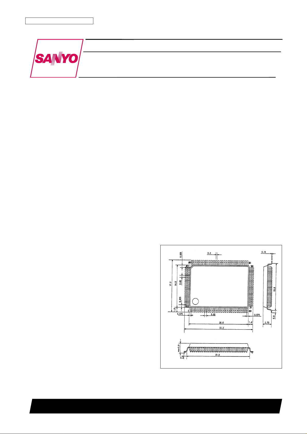
Package Dimensions
unit: mm
3151-QFP100E (FLP100)
CMOS LSI
13098HA(OT) No. 5692-1/32
SANYO: QIP100E (FLP100)
[LC78626E]
SANYO Electric Co.,Ltd. Semiconductor Bussiness Headquarters
TOKYO OFFICE Tokyo Bldg., 1-10, 1 Chome, Ueno, Taito-ku, TOKYO, 110-0005 JAPAN
DSP for Compact Disk Players
LC78626E
Ordering number : EN5692
Continued on next page.
Page 2

No. 5692-2/32
LC78626E
Continued from preceding page.
• Command (such as track jump, start focus, disk motor
start/stop, muting on/off, track count, etc.) is are
executed after they are entered from the microprocessor.
(An 8-bit serial input is used.)
• The digital output is equipped internally.
• High speed access is supported through discretionary
track counting.
• Using the 4× oversampling digital filter, D/A converter
signals with improved continuity of output data are
produced.
• A ∆∑-type D/A converter using a 3-order noise shaper is
equipped internally. (An analog low-pass filter is
equipped internally.)
• Internal digital attenuator (8-bit-[ALPHA]; 239 steps.)
• Internal digital deemphasis.
• Uses 0 cross mute.
• Bilingual compatibility.
• General I/O ports: 4. (Three of these are shared,
exclusively, with the subcode output function.)
• Up to ten seconds of skip prevention (when using 4M of
DRAM) through ADPCM compression/decompression
processing. 1M/4M bit DRAM can be selected.
• Memory overflow detection output.
• Free memory output.
Features
• 100-pin QFP
• A single 3.2 V/5 V power supply
Page 3
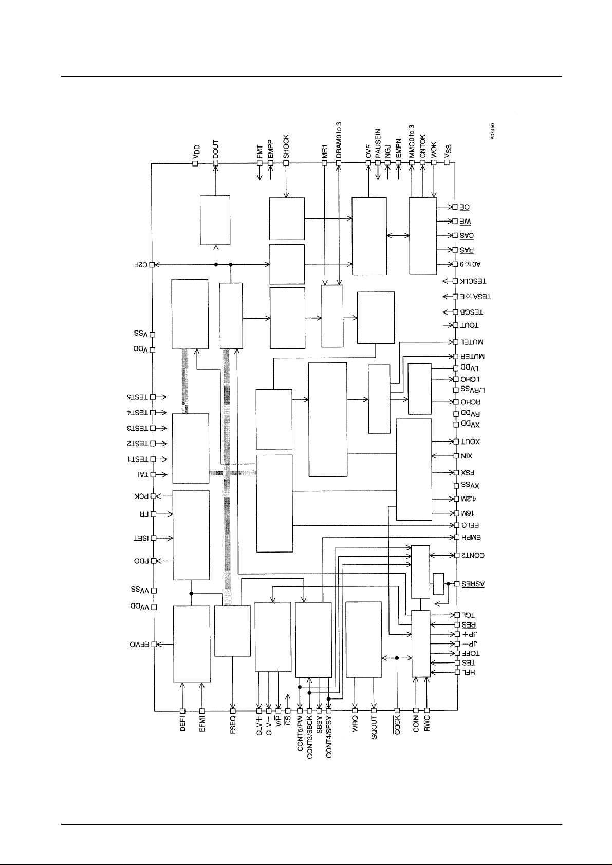
Equivalent Circuit Block Diagram
No. 5692-3/32
LC78626E
Digital out
RAM address
generator
Interpolation mute
Shock
detector
Contact
detector
ADPCM
encoder
Data width
changer
2K × 8-bit RAM
Digital
attenuator
4 × oversampling digital filter
C1, C2 error detection and
correction flag process
VCO clock production
clock control
Slice level control
Sync detect
EFM
demodulation
CLV digital servo
Subcode partition
QCRC
Microprocessor
interface
Servo commands
General ports
Disable
Crystal oscillator-system
timing generator
One-bit DAC
Low-pass
filter
ADPCM
decoder
DRAM control
Overflow process
initiation control
Page 4
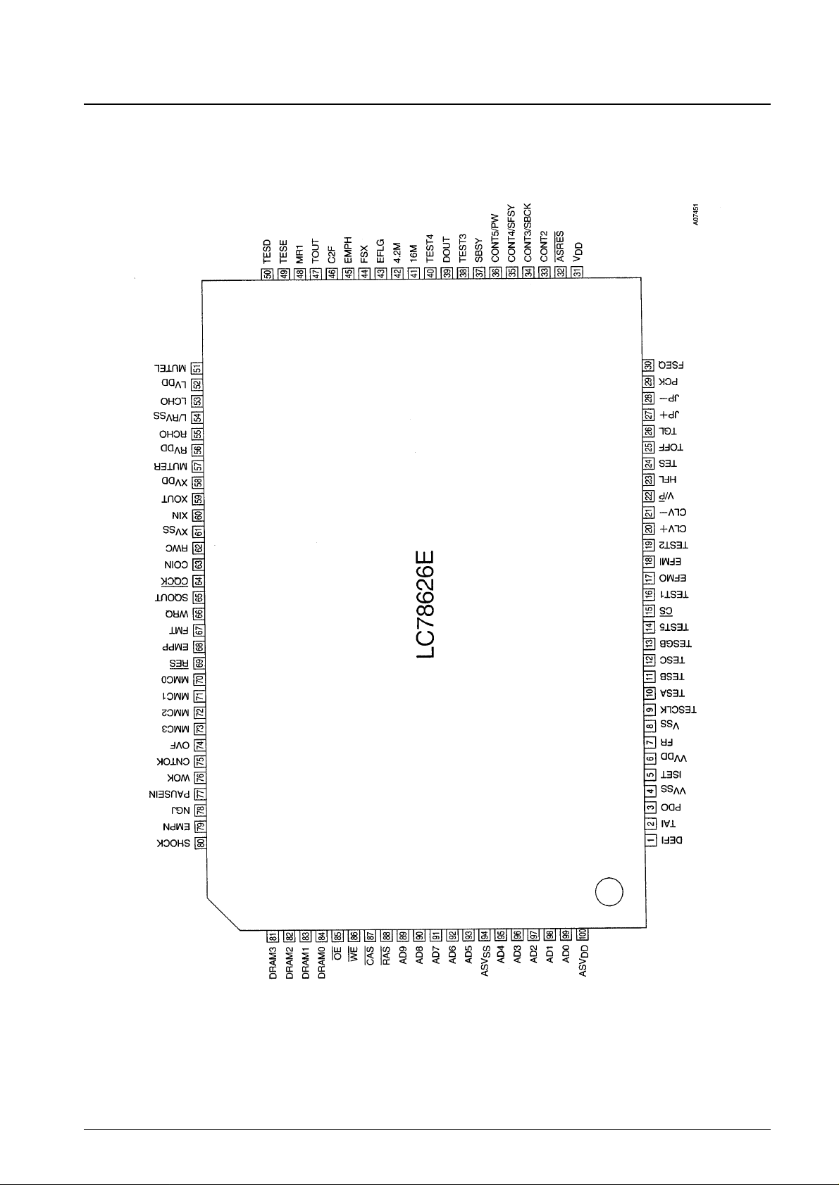
Pin Assignment
No. 5692-4/32
LC78626E
Top view
Page 5
No. 5692-5/32
LC78626E
Parameter Symbol Conditions Ratings Unit
Maximum power supply voltage V
DD
max VSS–0.3 to VSS+7.0 V
Input voltage V
IN
VSS–0.3 to VDD+0.3 V
Output voltage V
OUT
VSS–0.3 to VDD+0.3 V
Allowable power dissipation Pd max 400 mW
Operating temperature range Topr –20 to +75 °C
Storage temperature range Tstg –40 to +125 °C
Specifications
Absolute Maximum Ratings at Ta = 25°C, VSS= 0V
Parameter Symbol Conditions
Ratings
Unit
min typ max
V
DD
1
V
DD
, XVDD, LVDD, RVDD, VVDD:
3.0 5.5 V
Power supply voltage
ATT/DF/DAC to the normal speed
V
DD
2
V
DD
, XVDD, LVDD, RVDD, VVDD:
3.6 5.5 V
All functions guaranteed to 2× speed
V
IH
1
I/O and input pins with the exception of
0.7V
DD
V
DD
V
Input high level voltage
EFMI and DRAM0 to DRAM3
V
IH
2 EFMI 0.6V
DD
V
DD
V
V
IH
3 DRAM0 to DRAM3 0.45V
DD
V
DD
V
V
IL
1
I/O and input pins with the exception of
0 0.3V
DD
V
Input low level voltage
EFMI and DRAM0 to DRAM3
V
IL
2 EFMI 0 0.4V
DD
V
V
IL
2 DRAM0 to DRAM3 0 0.2V
DD
V
Data setup time t
SU
COIN, RWC: Figure 1 400 ns
Data hold time t
HD
COIN, RWC: Figure 1 400 ns
High level clock pulse width t
WH
SBCK, CQCK: Figures 1 to 3 400 ns
Low level clock pulse width t
WL
SBCK, CQCK: Figures 1 to 3 400 ns
Data read access time t
RAC
SQOUT, PW: Figures 2 and 3 0 400 ns
Command transfer time t
RWC
RWC: Figure 1 1000 ns
Subcode Q read enable time t
SQE
WRQ: Figure 2, no RWC signal 11.2 ms
Subcode ready cycle time t
SC
SFSY: Figure 3 136 µs
Subcode read enable time t
SE
SFSY: Figure 3 400 µs
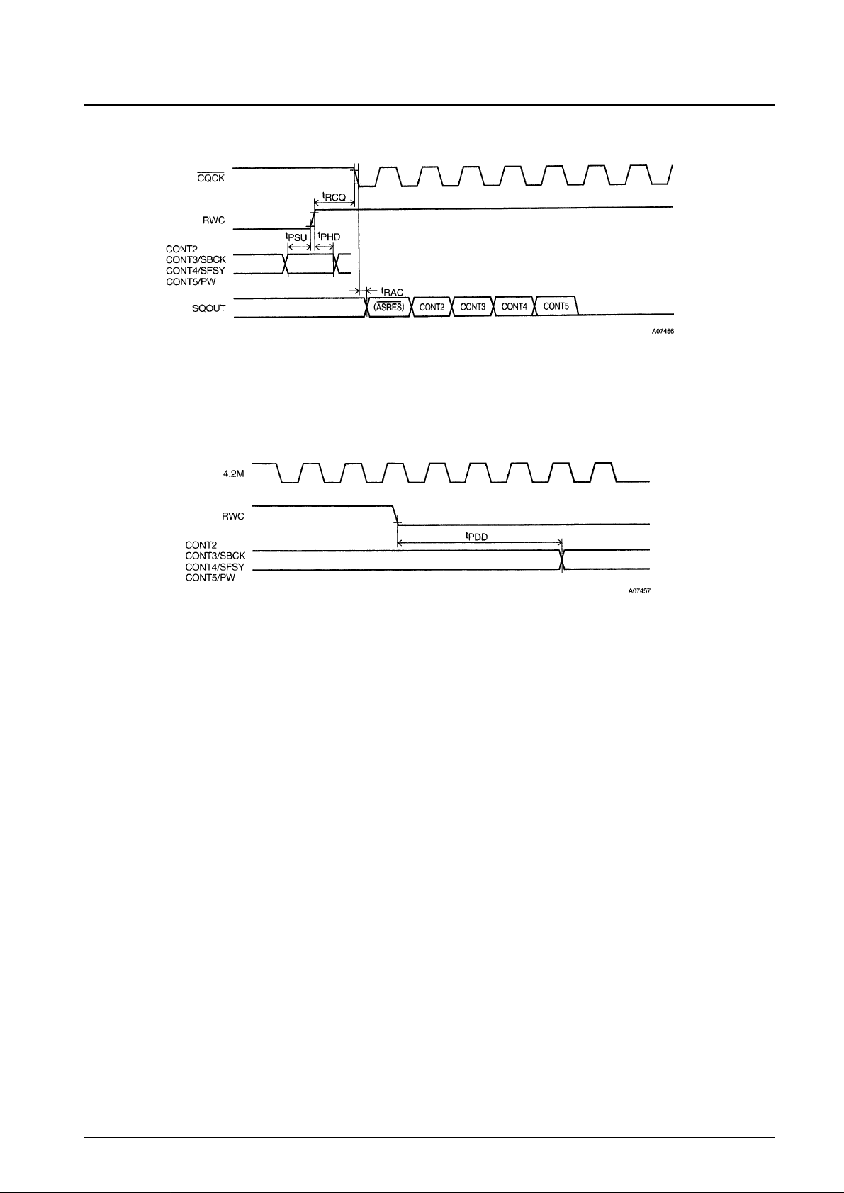
Port input data setup time t
CSU
CONT2 to CONT5, RWC: Figure 4 400 ns
Port input data hold time t
CHD
CONT2 to CONT5, RWC: Figure 4 400 ns
Port input clock setup time t
RCQ
RWC, CQCK: Figure 4 100 ns
Port output data delay time t
CDD
CONT2 TO CONT5, RWC: Figure 5 1200 ns
Input level
V
IN
1 EFMI: slice level control, VDD= 3.0 V 0.8 Vp-p
V
IN
2 XIN: C coupling input 1.0 Vp-p
Range of operating frequencies f
OP
EFMI 10 MHz
Crystal oscillator frequency f
X
XIN, XOUT 16.9344 MHz
Allowable Operating Range at Ta = 25°C, VSS= 0V
Parameter Symbol Conditions
Ratings
Unit
min typ max
Consumption current I
DD
VDD, XVDD, LVDD, RVDD, VVDD:
14 20 mA
V
DD
= 3.0 to 3.4 V with normal playback
DEFI, EFMI, HFL, TES, RWC, COIN, CQCK,
I
IH
1
FMT, MR1, RES, TESD, WOK, PAUSE IN,
5 µA
SHOCK, TESCLK, TESA, TESB, TESC,
Input high level current.
TESGB, TEST1: V
IN
= V
DD
IIH2
TAI, TEST2 to TEST5, CS, TESE:
15 55 µA
V
IN
= VDD= 3.4 V
Electrical Characteristics at Ta = 25°C, VDD= 3.2 V VSS= 0V
Continued on next page.
Page 6
No. 5692-6/32
LC78626E
Continued from preceding page.
Parameter Symbol Conditions
Ratings
Unit
min typ max
DEFI, EFMI, HFL, TES, RWC, COIN, CQCK,
FMT, MR1, RES, TESE, TESD, WOK,
Input low level current I
IL
PAUSE IN, SHOCK, TESCLK, TESA, TESB, –5 µA
TESC, TESGB, TAI, TEST1 to TEST5, CS :
V
IN
= 0 V
EFMO, CLV
+
, CLV–, V/P, TOFF, TGL, JP+,
V
OH
1 JP–, PCK, FSEQ, EFLG, FSX, EMPH : 2.56 V
I
OH
= –1 mA
CONT2 to CONT5, SBSY, MUTEL, MUTER,
Output high level current
VOH2 C2F, WRQ, SQOUT, 16M, 4.2M, EMPP, 2.56 V
OVF, CNTOK, NGJ : I
OH
= –0.5 mA
V
OH
3 DOUT : IOH= –12 mA 2.72 V
V
OH
4
OE, WE, CAS, RAS, AD9 to AD0, 256 V
DRAM3 to DRAM0 : I
OH
= –0.5 mA
V
OH
5 MMC0 to MMC3 : IOH= –2 mA 2.24 V
V
OL
1
EFMO, CLV
+
, CLV–, V/P, TOFF, JP+, JP–,
0.64 V
PCK, FSEQ, EFLG, FSX, EMPH : I
OL
= 1 mA
CONT2 to CONT5, SBSY, MUTEL, MUTER,
V
OL
2 C2F, WRQ, SQOUT, 16M, 4.2M, EMPP, 0.32 V
Output low level current
OVF, CNTOK, NGJ : I
OL
= 2 mA
V
OL
3 DOUT : IOL= 12 mA 0.48 V
V
OL
4
OE, WE, CAS, RAS, AD9 to AD0,
0.44 V
DRAM3 to DRAM0 : I
OL
= 0.5 mA
V
OL
5 MMC0 to MMC3 : IOL= 2 mA 0.96 V
PDO, CLV
+
, CLV–, JP+, JP–,
I
OFF
1 CONT2 to CONT5, DRAM0 to DRAM3, 5 µA
Output off leakage current
ASRES : V
OUT
= V
DD
PDO, CLV+, CLV–, JP+, JP–,
I
OFF
2 CONT2 to CONT5, DRAM0 to DRAM3, –5 µA
ASRES : V
OUT
= 0 V
Charge pump output current
I
PDOH
PDO : RISET = 68 kΩ 30 42 54 µA
I
PDOL
PDO : RISET = 68 kΩ –54 –42 –30 µA
Parameter Symbol Conditions
Ratings
Unit
min typ max
Total harmonic distortion rate TRD+N
LCHO, RCHO; 1 kHz: Uses the 0 dB data
0.015 0.018 %
input and the 20 kHz-LPF (in the AD725D).
LCHO, RCHO; 1 kHz: Uses the -60 dB data
Dynamic range DR input, the 20 kHz-LPF (in the AD725D), and 85 90 dB
the A filter.
LCHO, RCHO; 1 kHz: Uses the –0 dB data
Signal to noise ratio S/N input, the 20 kHz-LPF (in the AD725D), and 87 92 dB
the A filter.
Cross talk CT
LCHO, RCHO; 1 kHz: Uses the 0 dB data
79 82 dB
input and the 20 kHz-LPF (in the AD725D).
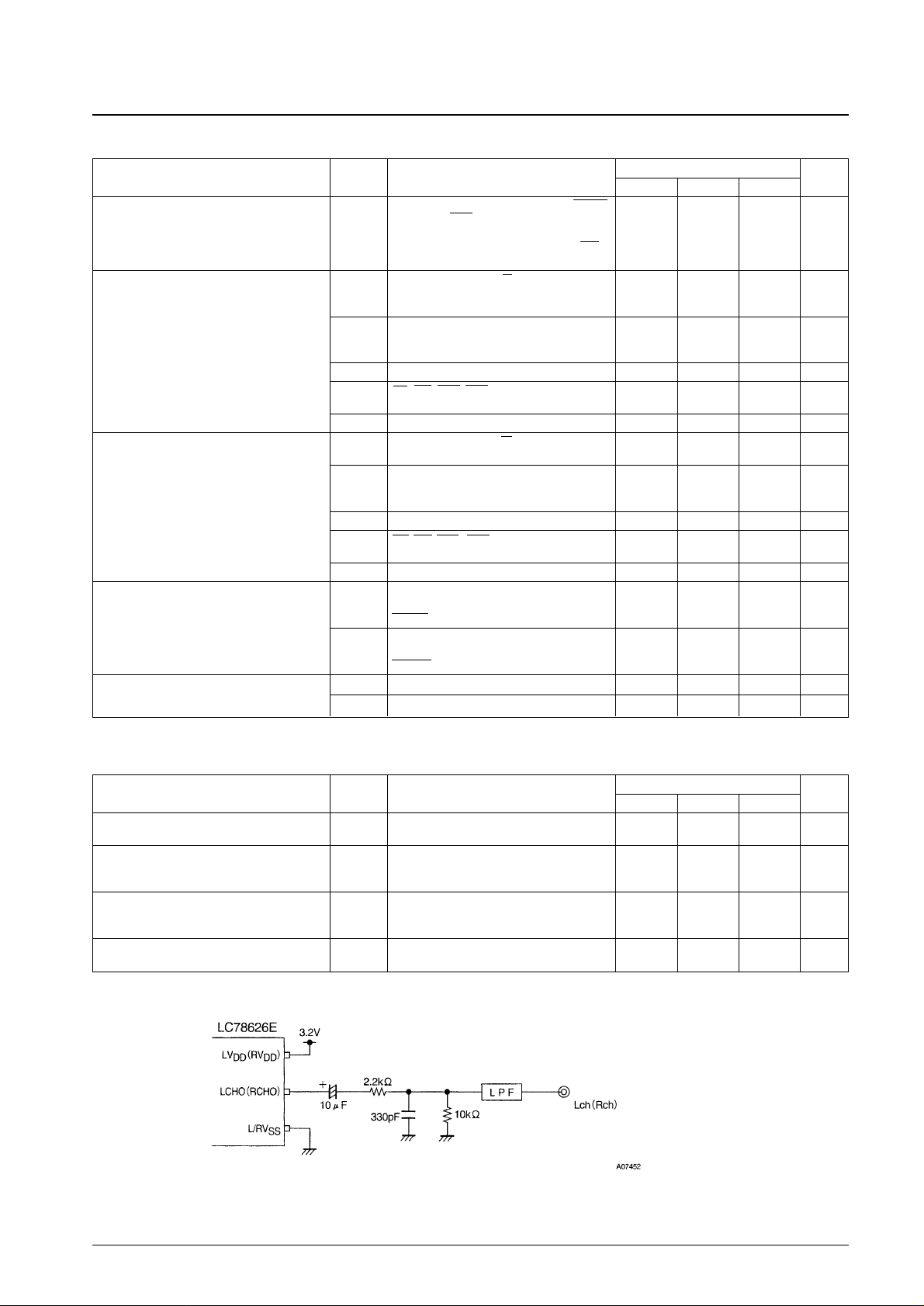
One-bit D/A Converter Analog Characteristics at
Ta = 25°C, VDD= LVDD= RVDD= 3.2 V, VSS= L/RVSS= 0 V
Analog output
Note: Measured with the normal-speed playback mode in the Sanyo one-bit D/A converter block reference digital attenuator circuit.
Page 7
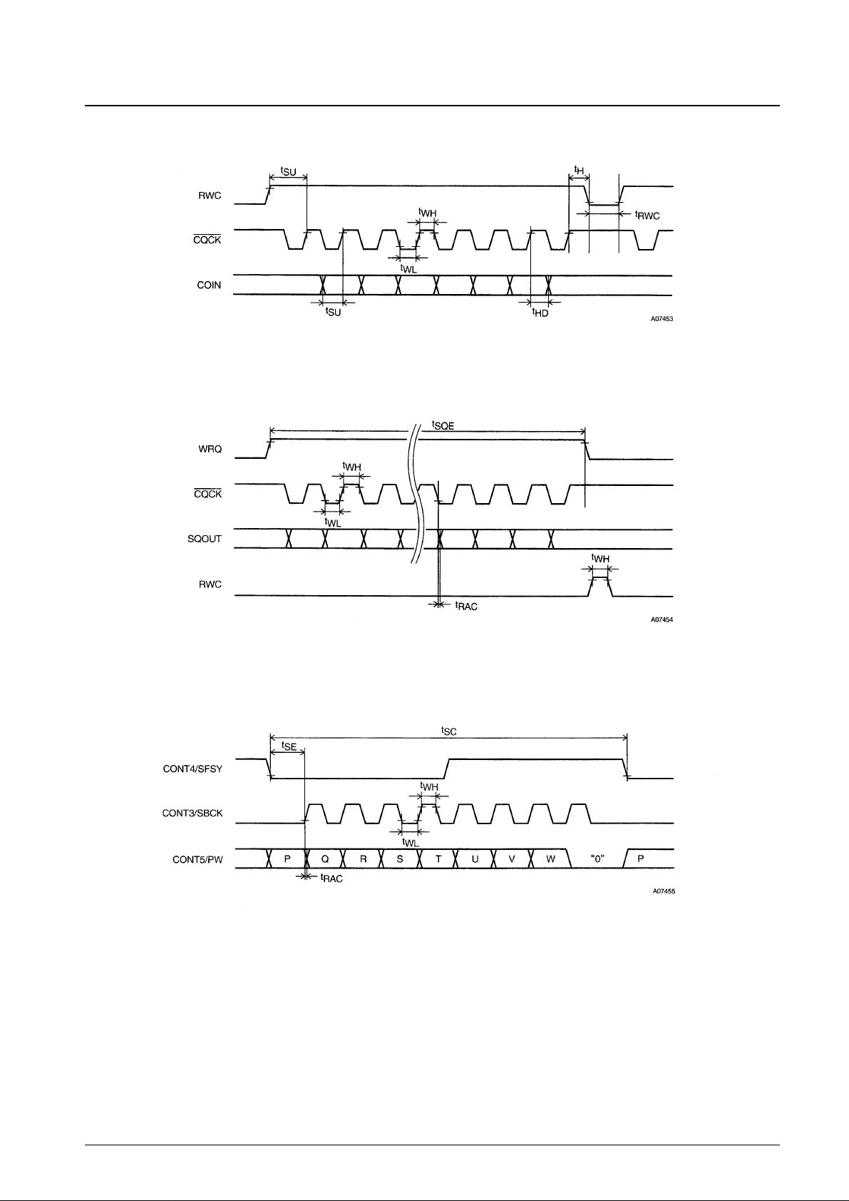
Figure 1 Command Input
Figure 2 Subcode Q Output
Figure 3 Subcode Output
No. 5692-7/32
LC78626E
Page 8
No. 5692-8/32
LC78626E
Figure 4 General Port Input Timing
Figure 5 General Port Output Timing
Page 9
No. 5692-9/32
LC78626E
Description of Pins
Pin Pin
I/O Function
No. Name
1 DEFI I Defect detection signal (DEF) input. When not used, must be connected to 0 V.
2 TAI I Test input. Equipped with internal pull-down resistor. Must be connected to 0V.
3 PDO O External VCO control phase comparator output.
4 VV
SS
P
For the PLL
Internal VCO ground. Must be connected to 0 V.
5 ISET AI PDO output current adjustment resistor connection.
6 VV
DD
P Internal VCO power supply.
7 FR AI VCO frequency range adjustment
8 V
SS
P Digital system ground. Must be connected to 0 V.
9 TESCLK I Test clock input. Must be connected to VDD.
10 TESA I Test operation mode control input. Must be connected to VDD.
11 TESB I Test operation mode control input. Must be connected to VDD.
12 TESC I Test operation mode control input. Must be connected to VDD.
13 TESGB I Test operation mode control input. Must be connected to VDD.
14 TEST5 I Test input. Equipped with internal pull-down resistor. Must be connected to 0 V.
15 CS I Chip select input. Equipped with internal pull-down resistor. When not controlled, must be connected to 0 V.
16 TEST1 I Test input. Must be connected to 0 V.
17 EFMO O For slice EFM signal output.
18 EFMI I level control. EFM signal input.
19 TEST2 I Test input. Equipped with internal pull-down resistor. Must be connected to 0 V.
20 CLV
+
O
Disk motor control output. Can have a 3-state output depending on the command.
21 CLV
–
O
22 V/P O
Rough servo/phase control automatic switching monitor output. If a high level then rough servo mode. If a low level then
phase control mode.
23 HFL I Track detect signal input. Schmidt input.
24 TES I Tracking error signal input. Schmidt input.
25 TOFF O Tracking off output.
26 TGL O Tracking gain switch output. Gain is increased with low level.
27 JP
+
O
Track jump control output. Can be 3-state output depending on the command.
28 JP
–
O
29 PCK O EFM data playback clock monitor. 4.3218 MHz during phase lock.
30 FSEQ O
Sync signal detect output. A high level when the sync signal detected from the EFM signal matches the internally
generated sync signal.
31 V
DD
P Digital system power supply.
Reset signal input for initializing only the anti-shock control part (i.e. excluding the DSP part). Resets when this
pin is low level, and release the reset when this pin is high level. Tie this pin to the low level (i.e., connected to 0 V) if
when using software control on the anti-shock part alone through the anti-shock part only reset disable/release
32 ASRES I(I/O) command ($F4) or the anti-shock only reset enable/inrush command ($F5).
Note: This pin is assigned as the least significant bit of the general I/O port however, use as a general I/O
pin is disabled. When the port I/O set command ($DB) is executed, the least significant bit is always “0,” and the
output driver is not turned ON.
33 CONT2 I/O
General I/O pin 2. This controls the commands from the microcontroller. When not used, either set this as an input
port and connect to 0 V, or set this as an output port and leave it open.
Continued on next page.
Page 10
No. 5692-10/32
LC78626E
Continued from preceding page.
Pin Pin
I/O Description
No. Name
General I/O pin 3. This controls the commands from the microcontroller. This pin is shared exclusively with
34 CONT3/SBCK I/O the subcode read clock input (SBCK). When not used, either set this as an input port and connect to 0 V, or set
this as an output port and leave it open.
General I/O pin 4. This controls the commands from the microcontroller. This pin is shared exclusively with
35 CONT4/SFSY I/O the subcode frame sync signal output (SFSY). When not used, either set this as an input port and connect to 0
V, or set this as an output port and leave it open.
General I/O pin 5. This controls the commands from the microcontroller. This pin is shared, exclusively, with
36 CONT5/PW I/O the subcode P, Q, R, S, T, U, V, W output (PW). When not used, either set this as an input port and connect to
0 V, or set this as an output port and leave it open.
37 SBSY O Subcode block sync signal output.
38 TEST3 I Test input. Equipped with an internal pull-down resistor. Must be connected to 0 V.
39 DOUT O Digital output. EIAJ format.
40 TEST4 I Test input. Equipped with an internal pull-down resistor. Must be connected to 0 V.
41 16M O 16.9344 MHz output.
42 4.2M O 4.2336 MHz output.
43 EFLG O C1, C2, one error, two error error correction monitor output
44 FSX O 7.35 kHz sync signal output (frequency divided from the crystal oscillator).
45 EMPH O Deemphasis monitor output. When high level, a deemphasis disk is being played back.
46 C2F O C2 flag output.
47 TOUT O Test output. Under normal operation, this should be left open.
48 MR1 I DRAM switch: high : 1M, low : 4M
49 TESE I Test input. Must be connected to 0V.
50 TESD I Test input. Must be connected to 0V.
51 MUTESL O L channel mute output.
52 LV
DD
P L channel power supply.
53 LCHO AO L channel output.
54 L/RV
SS
P
For the one-bit D/A
L/R channel ground. Must be connected to 0 V.
55 RCHO AO
converter
R channel output.
56 RV
DD
P R channel power supply.
57 MUTER O R channel mute output.
58 XVDD P Crystal oscillator power supply.
59 XOUT O
16.9344 MHz crystal oscillator connection.
60 XIN I
61 XVSS P Crystal oscillator ground. Must be connected to 0 V.
62 RWC I Read/write control input. Schmidt input.
63 COIN I Microcontroller command input.
64 CQCK I Input pin for the command input latch clock and the subcode readout clock. Schmitt input.
65 SQOUT O Subcode Q output.
66 WRQ O Subcode Q output standby output.
67 FMT I Operating mode switch: high: shock proof, low: through.
68 EMPP O DRAM empty (an RZP pulse is output when the DRAM is empty).
69 RES I External reset input: low reset (all internal blocks are reinitialized).
Continued on next page.
Page 11

No. 5692-11/32
LC78626E
Continued from preceding page.
PIn Pin
I/O Description
No. Name
70 MMC0 O Remaining DRAM output.
71 MMC1 O Remaining DRAM output.
72 MMC2 O Remaining DRAM output.
73 MMC3 O Remaining DRAM output.
74 OVF O DRAM write terminated. (An RZP pulse is output when there is an overflow or a shock.)
75 CNTOK O Data contact point detection complete signal: low→ high: detection complete. (DRAM write start).
76 WOK I DRAM write enable signal input: high: write enable.
77 PAUSE IN I Pause signal input: high: pause.
78 NGJ O C2F data contact point detection start signal: low → high: detection start.
79 EMPN O Remaining DRAM alarm output: low: memory low.
80 SHOCK I C2F shock detect pause signal input: low: pause shock detection.
81 DRAM3 I/O DRAM data bus
82 DRAM2 I/O DRAM data bus
83 DRAM1 I/O DRAM data bus
84 DRAM0 I/O DRAM data bus
85 OE O DRAM control signal.
86 WE O DRAM control signal.
87 CAS O DRAM control signal.
88 RAS O DRAM control signal.
89 AD9 O DRAM address bus
90 AD8 O DRAM address bus
91 AD7 O DRAM address bus
92 AD6 O DRAM address bus
93 AD5 O DRAM address bus
94 V
SS
P Digital system ground. Must be connected to 0 V.
95 AD4 O DRAM address bus
96 AD3 O DRAM address bus
97 AD2 O DRAM address bus
98 AD1 O DRAM address bus
99 AD0 O DRAM address bus
100 V
DD
P Digital system power supply.
Page 12

Pin Applications
1 The HF Signal Input Circuit Pin 18: EFMI, Pin 17: EFMO, Pin 1: DEFI, and Pin 20: CLV
+
When an HF signal is input to the EFMI, an EFM signal (NRZ),
sliced at the optimal levels, is obtained.
As a countermeasure against defects, when the DEFI pin (Pin 1)
is high, the slice level control output EFMO pin (Pin 17) goes to
a high impedance state, and the slice level is held. However, this
is only enabled when the CLV is in phase-control mode, or in
other words, when the V/P pin (Pin 22) is low. This can be
structured from a combination with the DEF pin of LA9230/40
series ICs.
* When the EFMI and CLV+signal lines are close to each other
then the error rate due to unnecessary radiation may increase.
It is recommended that these two lines be separated by a
ground line or by a VDDline as a shield line.
2 The PLL Clock Playback Circuit Pin 3: PDO, Pin 5: ISET and Pin 7: FR
The VCO circuit is equipped internally, and the PLL circuit is
structured using external resistors and external capacitors. The
ISET is the reference current for the charge pump. The PDO is
the loop filter for the VCO circuit, and the FR is the resistor that
determines the frequency range of the VCO.
Reference Values
R1 = 68 kΩ C1 = 0.1 µF (standard speed)
C1 = 0.047 µF (2× speed)
R2 = 680 Ω C2 = 0.1 µF
R3 = 5.1 kΩ
* It is recommended that a carbon coated resistor with a
tolerance of ± 5.0% be used for R3.
3 The VCO Monitor Pin 29: PCK
This is the monitor pin with an average frequency of 4.3218 MHz, which is a 1/2 frequency division from VCO.
4 The Sync Detect Monitor Pin 30: FSEQ
The EFM signal goes high when the frame sync signal (the true sync signal) from the PCK matches the timing (the
interpolated sync signal) generated by the counter. This serves as the sync detect monitor (holding the high level over
a single frame).
No. 5692-12/32
LC78626E
HF Signal
Frequency
and phase
comparator
Charge pump
Page 13

5 The Servo Command Functions Pin 62: RWC, Pin 63: COIN, Pin 64: CQCK
Various commands can be executed by setting RWC to high and by inputting the command from COIN synchronized
with the CQCK clock. The commands are executed beginning with the falling edge of RWC.
Focus start
Track jump
Mute control Single-byte commands
Disk motor control
Other control
Track check Two-byte command (two sets of RWC).
Digital attenuator
Two-byte commands (once set of RWC).
General port I/O settings
(1) Single-byte Commands
(2) Two-byte commands (RWC 2 set: for the track count)
(3) Two-byte commands (RWC 1 set: digital attenuation and setting the general I/O port)
(4) Eliminating Command Noise
This command makes it possible to reduce the noise that is mixed into the CQCK clock. This is effective for noise of
less than 500 ns; however, the CQCK timing must be set to have 1 µs or more for tWL, tWH, and tSU.
No. 5692-13/32
LC78626E
Code COMMAND RES = low
$EF Command input noise reduction mode
$EE Resets the command input noise reduction mode.
●●
Command ($F0, $F8)
Data ($08 to $FE), command ($FF)
At least 1 µs
Data Commands ($81 to $87, $DB, $DC)
Page 14

6 The CLV Servo Circuit Pin 20: CLV+, Pin 21: CLV-, Pin 22: V/P
CLV+is the signal for accelerating the disk in the forward direction, while CLV–is the signal for decelerating the
disk. Depending on the commands from the microcontroller, one of the following four modes is selected: Accelerate,
decelerate, CLV, or stop. The CLV+and CLV–outputs for each mode are as shown in the table below.
* The CLV servo control command is such that the TOFF pin is low only when the CLV mode is in effect, and it is high
otherwise. The TOFF pin control by the command is only active when the CLV mode is in effect.
(1) The CLV Mode
In the CLV mode the rotation of the disk is detected from the HF signal, and a precise linear speed of rotation is
derived by exerting the respective forms on control when the internal modes of the DSP change. The PWM frequency
is 7.35 kHz. The V/P has a high output when the internal mode is the rough servo, and a low output when the internal
mode is phase control.
(2) Switching the Rough Servo Gain
When the internal mode is the rough servo, the CLV control gain for the 8 cm disk can be reduced by 8.5 dB from the
level for the 12 cm disk.
No. 5692-14/32
LC78626E
Code COMMAND RES = low
$04 DISC MOTOR START (Accelerate)
$05 DISC MOTOR CLV (CLV)
$06 DISC MOTOR BRAKE (Decelerate)
$07 DISC MOTOR STOP (Stop) ●●
MODE CLV
+
CLV
–
Accelerate high low
Decelerate low high
CLV Pulse output Pulse output
Stop low low
Internal mode CLV
+
CLV
–
V/P
Rough servo (when the rotational speed is determined to be low) high low high
Rough servo (when the rotational speed is determined to be high) low high high
Phase control (when the PCK clock is running) PWM PWM low
Code COMMAND RES = low
$A8 DISC 8 cm Set
$A9 DISC 12 cm Set ●●
Page 15

(3) Switching the Phase Control Gain
By changing the frequency division value of the first-stage frequency divider of the phase comparator it is possible to
change the phase control gain.
(4) The CLV 3-state Output
The CLV 3-state output command makes it possible to control the CLV with a single pin. However, because this will
cause the spindle gain to fall by 6 dB, it will be necessary to increase the gain on the servo side.
No. 5692-15/32
LC78626E
Code COMMAND RES = low
$B1 CLV phase comparator 1/2 frequency division.
$B2 CLV phase comparator 1/4 frequency division.
$B3 CLV phase comparator 1/8 frequency division.
$B0 CLV phase comparator, no frequency division. ●●
Code COMMAND RES = low
$B4 CLV 3-state output
$B5 CLV 2-state output (traditional method) ●●
Phase
comparator
2-state output
3-state output
Acceleration
Deceleration
High impedance output
Page 16

(5) The Internal Brake Mode
* The internal brake mode is turned on by inputting the internal brake on command ($C5). When in this mode, when
the brake command ($06) is executed it becomes possible to monitor the state of deceleration of the disk using the
WRQ pin.
* In this mode, the status of deceleration of the disk is determined by counting the density of the EFM signals in a
single frame, and the CLV–is low if the number of EFM signals is 4 or less. At the same time, the WRQ signal is
put to high as the break complete monitor. The microcontroller issues the STOP command if it senses that the
WRQ signal is high, and thus brings the disk to a complete stop. In the internal break continuous mode the CLV–=
high brake operation continues even when the break complete monitor WRQ goes high.
When noise in the EFM signal causes the deceleration status to be judged incorrectly, it may be advisable to use the
internal break control command ($A3) to change the EFM signal count from 4 to 8.
* In the TOFF output inhibited mode ($CD), TOFF is low while the internal break is in operation. Its use is
recommended because it is effective in preventing incorrect detection at the mirrored surface of the disk.
* When there is a loss of focus during the execution of an internal break command it will be necessary to reissue the
internal brake command after the focus has been reestablished.
* Because there is a risk that the EFM signal will be discerned incorrectly depending on the playback status
(scratched disks, access processes, etc.), use in conjunction with the microcontroller is recommended.
* When the internal brake mode is in effect, then it is possible to monitor the disk deceleration status at the WRQ Pin
by executing the DISC MTR BRAKE command ($06) in this DSP. However, if another command is executed
while this command is in process, then the command will be aborted. When you wish to prevent the function from
being aborted, then, after issuing the DISC MTR BRAKE command ($06), do not issue any other commands until
a high WRQ signal is detected and the DISC MTR STOP command ($07) is issued.
7 The Track Jump Circuit Pin 23: HFL, Pin 24: TES, Pin 25: TOFF, Pin 26: TGL, Pin 27: JP+, Pin 28: JP
–
(1) Types of Track Counters
The following two track count modes have been provided.
The conventional track counter uses the TES signal itself as the internal track counter clock. In the new track count
method, however, the TES signal is combined with the HFL signal to reduce the amount of noise, producing a more
accurate track count through reducing the number of miscounts due to noise in the rising edge and falling edge of the
TES signal. However, when the HFL signal is absent because of dust, scratches, etc., there is the danger that there
will be no track count pulse, and thus caution is required when using this method.
No. 5692-16/32
LC78626E
Code COMMAND RES = low
$C5 Internal Break ON
$C4 Internal Break OFF ●●
$A3 Internal brake control
$CB Internal brake continuous mode
$CA Internal brake continuous mode reset ●●
$CD Internal brake TON mode
$CC Internal brake TON mode reset ●●
Code COMMAND RES = low
$22 The new track count (a combination of TES and HFL). ●●
$23 The conventional track count (direct count of the TES signal).
EFM signal
$06 command
Page 17

(2) The TJ Command
When the track jump command is input to the servo command an acceleration pulse is generated (period a), following
which a deceleration pulse is generated (period b), after which the specific jump is completed after the brake period
(period c) elapses. In this break period the beam slip direction is detected through the TES and HFL inputs, and the
segment of the TES signal that propagates the internal slip is cut by TOFF. Moreover, by increasing the servo gain
using TGL, it is possible to lock onto the track that is the jump destination. In the JP pulse interval TOFF output
mode, TOFF is high during the interval when the JP pulse is generated.
* The TOFF pin is only low when the CLV mode is active when related to the disk control mode, and this terminal is
high during start, stop, and break control. Moreover, the TOFF pin can be turned on and off independently using
commands. However, the disk motor control is only enabled when the CLV mode is active.
No. 5692-17/32
LC78626E
Code COMMAND RES = low
$A0 The conventional track jump ●●
$A1 The new track jump.
$11 1 TRACK JUMP IN #1
$12 1 TRACK JUMP IN #2
$31 1 TRACk JUMP IN #3
$52 1 TRACK JUMP IN #4
$10 2 TRACK JUMP IN
$13 4 TRACK JUMP IN
$14 16 TRACK JUMP IN
$30 32 TRACK JUMP IN
#15 64 TRACK JUMP IN
$17 128 TRACK JUMP IN
$19 1 TRACK JUMP OUT #1
$1A 1 TRACK JUMP OUT #2
$39 1 TRACK JUMP OUT #3
$5A 1 TRACK JUMP OUT #4
$18 2 TRACK JUMP OUT
$1B 4 TRACK JUMP OUT
$1C 16 TRACK JUMP OUT
$38 32 TRACK JUMP OUT
$1D 64 TRACK JUMP OUT
$1F 128 TRACK JUMP OUT
$16 256 TRACK CHECK
$0F TOFF
$8F TON ●●
$8C TRACK JUMP BRAKE
$21 JP pulse period TOFF output mode.
$20 JP pulse period TOFF output mode reset. ●●
(Brake period)
(JP pulse period)
Page 18

(3) The TJ Mode
The relationships between the acceleration pulse, deceleration pulse, and brake interval are as shown in the table
below.
* The 256 TRACK CHECK does not produce an actuator drive signal as shown in the table above, rather because the mode is such that the TES signal is
counted when the tracking loop is off, it is necessary to provide a feed to the feed motor.
* When the track jump sequence (a, b, c) is completed, the servo command register is reset automatically.
* When a new command has been input when the track jump is in process, that command is executed at that instant.
* In the 1 TRACK JUMP #3 command there is no brake period (period c), but rather caution is warranted because it is necessary to generate the brake
mode using an external circuit.
* Although in the 2TRACK JUMP IN (OUT) of the new track jump mode the brake period (period c) did not exist for the LC78620E/21E/25E ICs, in this IC
period C has been changed to 60 ms.
No. 5692-18/32
LC78626E
Command
When in the conventional track jump mode When in the new track jump mode.
a b c a b c
1 TRACK JUMP IN (OUT) #1 233 µs 233 µs 60 ms Same as in the conventional mode.
1 TRACK JUMP IN (OUT) #2
0.5 TRACK
233 µs 60 ms
0.5 TRACK The same
60 ms
JUMP period JUMP period as for a
1 TRACK JUMP IN (OUT) #3
0.5 TRACK
233 µs
This period 0.5 TRACK The same This period
JUMP period does not exist JUMP period as for a does not exist
1 TRACK JUMP IN (OUT) #4
0.5 TRACK
233 µs
60 ms TOFF =“L” 0.5 TRACK The same 60 ms TOFF =“L”
JUMP period during period C JUMP period as for a during period C
2 TRACK JUMP IN (OUT) None
1 TRACK The same
60 ms
JUMP period as for a
4 TRACK JUMP IN (OUT)
2 TRACK
466 µs 60 ms
2 TRACK The same
60 ms
JUMP period JUMP period as for a
16 TRACK JUMP IN (OUT)
9 TRACK 7 TRACK
60 ms
9 TRACK The same
60 ms
JUMP period JUMP period JUMP period as for a
32 TRACK JUMP IN (OUT)
18 TRACK 14 TRACK
60 ms Same as in the conventional mode.
JUMP period JUMP period
64 TRACK JUMP IN (OUT)
36 TRACK 28 TRACK
60 ms Same as in the conventional mode.
JUMP period JUMP period
128 TRACK JUMP IN (OUT)
72 TRACK 56 TRACK
60 ms Same as in the conventional mode.
JUMP period JUMP period
TOFF is high during the period over
256 TRACK JUMP IN (OUT) which 256 tracks elapse and pulses a 60 ms Same as in the conventional mode.
and b are not produced.
TRACK JUMP BRAKE There is no a or b period. 60 ms Same as in the conventional mode.
Slip detector
High during the brake interval
Page 19

The THLD Signal is generated on the LA9230M, 9240M Series side, and causes the tracking error signal to be held
during the JP pulse period.
* The Tracking Brake
The relationship between the TES, HFL, and TOFF signals during the track jump period c is as shown below. The
TOFF signal is generated from the HFL signal with the changing edge of the TES signal. The high of the HFL signal
is for the mirrored area, while the low is for the pitted area. As the beam sweeps from the mirrored surface to the
pitted area, TOFF becomes high, and as the beam sweeps from the pitted area to the mirrored surface, TOFF is made
low in the gain-enhanced state (TGL low), and the brake is applied.
(4) The JP 3-state Output
Using the JP 3-state command, the track jump can be controlled with a single pin, however, the gain must be
increased on the servo side because the kick gain will decrease by 6 dB.
(5) The Track Check Mode
After the track check IN or track check OUT command has been entered, then when a discretionary number between
8 and 254 is entered as binary data, a track count of the specified number - 1 will be performed.
No. 5692-19/32
LC78626E
Code COMMAND RES = low
$B6 JP 3-state output
$B7 JP 2-state output (conventional method) ●●
Code COMMAND RES = low
$F0 Track check IN
$F8 Track check OUT
$FF Two byte command reset ●●
TES (when moving towards the outside)
TES (when moving towards the inside)
HFL
TOFF output
2-state output
3-state output
High impedance output
The number of desired track checks = the number of track checks input – 1
Command
Track check
Track check
In/Out command
Binary input of the desired
number of tracks + 1
Double byte
command reset
Rising edge at the
number of tracks/2
Goes low when the track
check is complete.
Brake command
Page 20

* When the desired number of tracks is entered as a binary number, the track check operation begins with the falling
edge of the RWC.
* During the track check the TOFF pin becomes high and the tracking loop turns off, and thus there is the need to
provide a feed to the feed motor.
* When the track check In/Out commands are entered, the WRQ signal changes from the subcode Q standby monitor
that it is during normal times to become the track check monitor. This signal becomes high when half of the number
of tracks have been checked, and becomes low when the check is complete. The microcontroller sees that the WRQ
signal has become low and determines that the check has been completed.
* If the two-byte reset command is not entered, the track check operation begins again. In other words, if you wished to
advance 20,000 tracks, then a single 201 track check code would be sent and then when 100 cycles of the WRQ have
been counted, then there have been 20,000 track checks.
* When the track check is performed, the brake command is used to lock the pickup to a track.
8 The Error Flag Output Pin 43: EFLG, Pin 44: FSX
The FSX is the 7.35 kHz frame sync signal that is created by frequency dividing the crystal clock. For each frame, the
error correction status is output to EFLG. It is easy to tell the quality of the playback by the number of high pulses
that appear in the EFLG signal.
9 The Subcode P, Q and R to W Output Circuits Pin 34: SBCK, Pin 35: SFSY/CONT4, Pin 36: PW/CONT5,
Pin 37: SBSY
PW is the subcode signal output pin. (Note: Pin 35 and Pin 36 are, respectively, a general I/O pin and an exclusively
shared pin, and the selection of the pin depends on commands from the micro controller. See Item 19 on page 24.) By
applying 8 clocks to SBCK within 136 µs of the falling edge of SFSY, it is possible to read all codes until P, Q, and R
to W. The signal that appears at the PW pin changes with the rising edge of SBCK. When no clock is applied to
SBCK, the “P” code is output to PW. SFSY is a signal that is output for each subcode frame, and the falling edge of
this signal indicates that the subcode symbol (P to W) output is in standby. The subcode data P is output at the falling
edge of this signal.
SBSY is a signal output for each subcode block. This signal becomes high during sync signals S0 and S1, and its
falling edge indicates the end of the subcode sync signal and the beginning of the data in subcode block (in EIAJ
format).
No. 5692-20/32
LC78626E
1 correction
2 correction
Correction
function
No errors
Page 21

10 The Subcode Q Output Circuit Pin 66: WRQ, Pin 62: RWC, Pin 65: SQOUT, Pin 64: CQCK, Pin 15 CS
It is possible to read the subcode Q from the SQOUT pin by inputting a clock into the CQCK pin. Of the 8-bit
subcodes, the “Q” signal is useful in accessing musical selections, in displays, etc. WRQ is only high when the CRC
has been passed and the address in the subcode Q format is “1.” (See Note 1.) When the microcontroller detects this
high level, it can transmit a CQCK signal to read the data from SQOUT in the order shown below. When the CQCK
transmission begins, data changes in the internal registers of the DSP are inhibited. Once the microcontroller has
completed its read, RWC temporarily goes high, enabling data updating. At this time, WRQ goes low. Because WRQ
goes low after being high for 11.2 ms, the CQCK input starts during the interval when WRQ is high. The data can be
read beginning with the least significant bit.
Note 1: This conditions is ignored if an address-free command is sent (corresponding to the CDV).
The items within the parentheses are for the read-in area.
* The WRQ pin normally indicates the subcode Q standby; however, when in the track counter mode and when there is
an internal bake, it becomes a different monitor. (See the track count and internal brake items.)
* This IC becomes active when the CS pin is low, and the subcode Q data is output from the SQOUT pin. When the CS
pin is high, the SQOUT pin enters a high impedance state.
No. 5692-21/32
LC78626E
Code COMMAND RES = low
$09 ADDRESS FREE
$89 ADDRESS 1 ●●
CONT ADR
TNO
INDEX (POINT)
MIN
SEC
FRAME
ZERO
AMIN (PMIN)
ASEC (PSEC)
AFRAME (PFRAME)
Sub Q data
Page 22

11 The Bilingual Function
* At reset or when a stereo command ($28) has been entered, Lch and Rch are output, respectively, to Lch and Rch.
* When the Lch set command ($29) is entered, the Lch data is output to both Lch and Rch.
* When the Rch set command ($2A) is entered, the Rch data is output to both Lch and Rch.
12 Deemphasis Pin 45: EMPH
Of the subcode Q control data, the pre-emphasis On/Off bit is output from the EMPH pin. When this pin is high, the
deemphasis circuit within this IC is activated, and the D/A converter output are de-emphasized.
13 The Digital Attenuator
It is possible to apply digital attenuation to the audio data by setting the RWC high and inputting from the COIN a
two byte command synchronized with the CQCK clock.
After reset, the attenuation level is set to “MUTE” (the attenuation coefficient is 00H, where MUTE = –∞), and thus
it is necessary to directly set the attenuation coefficient EEH using the direct set (ATT DATA SET) command in
order to produce a sound. The attenuation level can be set to a range from 00H to EEH (239 different levels) by the
microcontroller commands.
This two byte command is different from the two byte commands used in track counting in that RWC only needs to
be set once, and it is not necessary to reset the two byte command either. (See the two byte command RWC1 set on
page 13.)
After inputting the target attenuation level in terms of 00H to EEH, then if the attenuate step-up/step-down
commands are transmitted, the system steps closer to the target with the corresponding step size of 4, 8, or 16,
synchronized with the rising edge of LRSY. However, when the ATT DATA SET command has been used, then the
target value is set directly. When new data is entered during the transition, then the target value is approached from
whatever value is in effect at that time. Caution is required when using the step-up/step-down commands at this time.
No. 5692-22/32
LC78626E
Code COMMAND RES = low
$28 STO CONT ●●
$29 Lch CONT
$2A Rch CONT
Code COMMAND RES = low
$81 ATT DATA SET DATA 00H Set
$82 ATT 4STEP UP (MUTE –∞dB)
$83 ATT 4STEP DOWN
$84 ATT 8STEP UP
$85 ATT 8STEP DOWN
$86 ATT 16STEP UP
$87 ATT 16STEP DOWN
Command
Attenuation data 00H to EEH
Attenuate set command
Page 23

ATT DATA
The audio output level = 20 log ————— [dB]
100H
Because, for example, the time that it would take to increase the attenuation level from “00H” to “EEH” using the 4
step-up command would be as calculated below, this amount of time must be left before entering the next attenuation
level command:
238 level × 4 Step-up
————————— ≈ 21.6 ms (approx.)
44.1 kHz (LRSY)
* In order to prevent noise due to arithmetic overflow in the one-bit D/A converter, settings greater than EEH are
prohibited.
14 The Mute Output Pin 51: MUTEL, Pin 57: MUTER
When the Mute control (MUTE –∞ dB: $03) is exerted, and once the data for each channel has been continuously at
“0” for a specified amount of time, then this output goes high. Afterwards, when data is again entered, this output
immediately goes low.
15 The C2 Flag Output Pin 46: C2F
C2F is an 8-bit unit flag that indicates the data error status.
16 The Digital OUT Output Circuit Pin 39: DOUT
This is the digital audio interface output pin. Its output is in EIAJ format. This signal is interpolated, and the signal is
output through the MUTE circuit. Because this output pin is equipped with an internal driver, it can drive a
transformer directly.
* The digital OUT pin can be fixed low by inputting the DOUT OFF command.
* Of the DOUT data, the UBIT data can be fixed at low by entering the UBIT OFF command.
* By entering the CDROM-XA command, the DOUT pin can be switched to CD-ROM data that is not subjected to
interpolation or to mute control. (When this is done, the audio output is put into mute mode.) The ROMXA-RST
command returns the DOUT pin to the audio data output mode which is subject to interpolation and mute control.
(When this is done, the audio output mute is released.)
17 The Mute Control Circuit
The sound level can be muted (MUTE –∞ dB) by the entry of the commands above. Because zero cross mute is used,
there is little noise during this operation. The zero cross determination is made in the range where the most significant
7 bits are all “1” or all “0.” Because the MUTE–12 dB command ($02) that was found in the LC78620E and 78621E
has been deleted, the digital attenuator is used and ATT DATA = 60 ($3C) is set.
No. 5692-23/32
LC78626E
Code COMMAND RES = low
$42 DOUT ON ●●
$43 DOUT OFF
$40 UBIT ON ●●
$41 UBIT OFF
$88 CDROM-XA
$8B ROMXA-RST ●●
Code COMMAND RES = low
$01 MUTE 0 dB
$03 MUTE –∞ dB ●●
44.1 kHz (normal speed), 88.2 kHz (double speed)
Start
Stop
Page 24

18 The Interpolation Circuit
If, when the error correction circuit cannot correct an error, the erroneous audio data is output without any correction,
the result would be excessive noise. In order to reduce this noise, the erroneous data is replaced with a linear
approximation based on the correct data on either side of the incorrect data. When there are two or more C2 flags, the
previous data level is held. However, when new data is output after two or more continuous flags, then a linear
approximation is made based on the correct data and the held value that is two points earlier and the middle point is
replaced with this linear approximation.
19 The General I/O Ports Pin 33: CONT2, Pin 34: CONT3, Pin 35: CONT4/SFSY, Pin 36: CONT5/PW
The four signal lines, CONT2 to CONT5, have I/O ports. These lines are all input terminals at the time of reset.
Unused ports must either be connected to ground or set as output ports. Moreover, pins 35 and 36 are pins that are
shared (exclusively) as, respectively, the subcode frame sync signal output pin (SFSY) and the subcode output pin
(PW). The selection of the function of these pins is done by commands from the microcontroller.
The port data is read out sequentially from CONT2, CONT3, CONT4, and CONT5 with the falling edge of the
CQCK from the SQOUT pin when there is a port read command. The command uses a single-byte command format.
* When a command is applied to this DSP during a track check, track jump, or internal MTR brake operation, then the
DSP will terminate those operations. If you do not wish to terminate these operations, do not apply unnecessary
commands (including general port operation commands) during track check, track jump, or internal MTR brake
operations.
These ports can each be set individual as control output ports by the port I/O set command. The ports are selected by
the lower four bits of a single byte. Starting with the least significant bit, these four bits of this single byte data
correspond to CONT2, CONT3, CONT4, and CONT5. The command uses a two-byte command format (RWC1 set).
No. 5692-24/32
LC78626E
Code COMMAND RES = low
$DD PORT READ
$DB PORT I/O SET PORT I SET
$DC PORT OUTPUT
Code COMMAND RES = low
$F6 SFSY, PW output enabled
$F7 SFSY, PW output disabled ●●
(1) When there is an error in one place
Correct data
Flagged data
Interpolated data
Held at the previous value.
(2) When there are continuous errors (three errors in this example).
Page 25

dn = 1: Set CONTn to be an output pin
dn = 0: Set CONTn to be an input pin.
Where n = 2 to 5
The ports that are set to output pins then they can independently output either high or low levels. The lower four bits
of the single byte of data correspond to the respective ports. Starting with the least significant bit of this single byte of
data, the bits correspond to CONT2, CONT3, CONT4, and CONT5. The command uses a two-byte command format
(RWC1 set).
dn = 1: Outputs a high level from the CONTn that is set to being an output
dn = 0: Outputs a low level from the CONTn that is set to being an output
20 The Clock Oscillator Pin 60: XIN, Pin 59: XOUT
By connecting a 16.9344 MHz oscillator to these pins a clock is generated that serves as the time base.
The OSC OFF command is a command to stop the oscillation of the oscillator and the VCO oscillation. Moreover,
depending on the command, double speed playback is also possible.
(1) When structuring a double speed playback system, connect a 16.9344 MHz oscillator between the XIN (Pin 60) and
the XOUT (Pin 59), and set the playback speed using the double speed playback command.
(2) Recommended crystal/ceramic oscillator constants.
The load capacitance Cin and Cout will have different requirements depending on the actual print circuit board used,
and thus it is necessary to perform verification testing on the use print circuit board. Consult the oscillator
manufacturer.
21 The 16M and 4.2M Pins Pin 41: 16M, Pin 42: 4.2M
When using double speed/normal speed playback mode, a 16.9344 MHz signal will be output from the 16M pin after
the external crystal oscillator 16.9344 MHz. A 4.2336 MHz will be output constantly from the 4.2M pin, forming a
LA9230/40 Series LSI system clock. When OSC is OFF, both terminals are constantly either high or low.
No. 5692-25/32
LC78626E
Single-byte data + $DB PORT I/O SET
Single-byte data + $DC PORT OUTPUT
Code COMMAND RES = low
$8E OSC ON ●●
$8D OSC OFF
$CE XTAL 16M ●●
$C2 Normal speed playback ●●
$C1 Double speed playback
Manufacturer Product No. Load Capacitance Dumping Resistance
C1/C2 (C1 = C2) Rd
CITIZEN WATCH CO., LTD.
CSA-309 (16.9344 MHz) 6 pF to 10 pF (±10%) 0Ω
(Crystal Oscillator)
TDK, Ltd. FCR 16.93M2G (16.93 MHz) 15 pF (±10%) 100Ω (±10%)
(Ceramic oscillator) FCR 16.93MCG (16.93 MHz) 30 pF (Internal type) 47Ω (±10%)
Oscillator
(C1)
(C2)
Page 26

22 The Reset Circuit Pin 69: RES
When the power supply is turned on, first set this pin low and then set it to high. The muting is set to –∞dB and the
disk motor is set to stop.
When the RES pin is low, then the statuses found in the boxes above are set directly.
23 Other Pins Pin 2: TAI, Pin 16: TEST1, Pin 19: TEST2, Pin 38: TEST3, Pin 40: TEST4, Pin 14: TEST5
These are pins for testing the circuits within the IC. While TAI and TEST1 to TEST5 are equipped with internal pulldown resistors, for safety reasons, they should be connected to 0 V.
24 Explanation of the Block Functions
(1) RAM Address Control
This IC contains 8 bits × 2K words on on-board RAM, and, depending on the address control, the EFM modulation
data jitter absorption capability can have ± 4 frames as the buffer memory capacity. Moreover, normally this buffer
margin is checked, and by precisely controlling the CLV servo circuit PCK-side frequency ratio it is possible to
control the data write address so that it will be centered on the size of the buffer. Also, when the ± 4 frame buffer
capacity is exceeded, the write address can be forced to ± 0, and because the resulting errors cannot be subjected to
flag processing, the mute is applied for a 128 frame period.
No. 5692-26/32
LC78626E
CLV servo relationship START STOP BRAKE CLV
Muting control 0dB –∞
Subcode Q address parameter Address1 Address Free
Track jump mode Conventional New
Track count mode Conventional New
Digital attenuator DATA0 DATA 00H to EEH
OSC ON OFF
Playback speed Normal speed Double speed
Digital filter normal speed ON OFF
Position Frequency Divider Ratio or Process
–4 or lower Forces transition to ± 0
–3 589
–2 589 Forward frequency division
–1 589
±0 588 Standard frequency division
+1 587
+2 587 Backwards frequency division
+3 587
+4 or greater Forces transition to ± 0
Page 27

(2) C1 and C2 Corrections
Data that has been EFM modulated is written to the internal RAM, the jitters are absorbed, and then, the following
processes are performed with uniform timing through the crystal oscillator clock. First, there is error checking and
correction as the C1 block, the C1 flag is determined and written to the C1 flag register. Next, error checking and
corrections are performed as the C2 block, and the C2 flag is determined and written to the internal RAM.
Note: 1. If the error position determined by the C2 check matches the C1 flag, then the error correction is performed and the flag is reset. However, when
there are seven or more C1 flags, then there would be the risk of an erroneous correction, and thus no correction is performed and the C1 flags
become C2 flags. When one of the error positions match, but another error position does not match, then no correction can be performed. Moreover,
when there are five or less C1 flags, then the C1 check is thought to be somewhat dubious, and thus the flag is set. When there are six or more, the
error correction is not possible and they are handled together, so the C1 flags become C2 flags as they are. When none or the error positions match,
naturally error correction cannot be performed, and when the number of C1 flags is two or less, then there may be errors even in the data that was
deemed OK by the C1 check, and thus the flag is set. In other cases, the C1 flags are used as C2 flags as they are.
2. When it is determined that error correction is not possible because there are three or more errors, then naturally error correction cannot be
performed and when the number of C1 flags is two or less, even the data that was deemed as OK in the C1 check may contain errors, and thus the
flags are set. In other cases, the C1 flags are used as C2 flags directly.
25 The Anti-shock Function Pin 67: FMT, Pin 48: MR1, Pin 76: WOK, Pin 75: CNTOK, Pin 74: OVF, Pin 46:
C2F, Pin 66: WRQ, Pin 65: SQOUT
The anti-shock function of this IC reads data from the disk at double speed and stores it in the external DRAM. By
replaying that data that was stored when an external shock has caused the data acquisition to be defective, it is
possible to avoid defective playback due to external shocks. The anti-shock mode is set by placing the FMT pin high.
When the data is stored in external DRAM, the 16-bit data is compressed to 5 bits using ADPCM. Depending on the
DRAM capacity (256K x 4 bits or 1M x 4 bits) the time that can be stored will be approximately 2.4 seconds (1M) or
approximately 9.5 seconds (4M). Depending on the type of DRAM, the MR1 might have to be set. (See the table.)
When in the anti-shock mode, the double speed data is written to the external DRAM and then read at normal speed
(1x speed) for playback, and thus the external DRAM will eventually become full. When this happens, this IC stops
writing to the DRAM and places the OVF pin high. The microcontroller monitors the OVF and when the
microcontroller senses that the OVF signal has gone high, it places the WOK pin low and in order to find the point at
which the writing was terminated (called the "L" point below) the system must perform a track jump. The
microcontroller has already determined through its monitoring of the frame number in the subcode Q the location of
the L point. The frame number at the point when the OVF pin becomes high track jumps to the location, and the L
point is sought by placing the WOK pin high that many frames earlier. When this IC finds the L point, the CNTOK
pin is put high, and the DRAM data write process begins again. Furthermore, sometimes the L point cannot be found,
such as when there is an external shock during the L point search. If the CNTOK pin has not become high even if the
L point frame number has been passed (by three or more frames), then it is determined that the L point was not found.
When this happens, a track jump is performed again, and the L point search begins again. When the search is
performed again, the track jump is performed with the WOK pin High. This IC determines whether or not there has
been an external shock through the use of the C2F flag. When the C2F flag becomes high then the OVF pin becomes
high just as if the DRAM was full, and writing to the DRAM is terminated. In this case, the microcontroller should
perform the same process as if the DRAM had become full.
No. 5692-27/32
LC78626E
C1 Check Correction and Flag Process
No error Correction not required/flag is reset
1 error Correction performed/flag is reset
2 errors Correction is performed and flag is set
3 or more errors Correction is not possible and flag is set
C2 Check Correction and Flag Process
No error Correction not required/flag is reset
1 error Correction performed/flag is reset
2 errors See the C1 flag. (Note 1)
3 or more errors See the C1 flag. (Note 2)
The Setting pins
Pin High Low
FMT Anti-shock mode: ON Anti-shock mode: OFF
MR1 1M bit (256K × 4 bit) DRAM 4M bit (1M × 4 bit) DRAM
Page 28

A Schematic of the timing of the various signals during the anti-shock operations are shown in the figure below.
26 Anti-shock Independent Reset
It is possible to initialize only the anti-shock controller part (excluding the DSP part) by setting the ASRES pin to
low. The reset is released by setting this pin high. Furthermore, when controlling the independent reset using
commands, the ASRES pin must be tied low (connected to 0 V).
No. 5692-28/32
LC78626E
Code COMMAND RES = low
$F4 Independent reset disable (release)
$F5 Independent reset enable/inrush ●●
Beginning of L point search
L point is found. Beginning of writing to the DRAM
L point because of shock
Track jump
L point because the DRAM is full
Track jump
Page 29

27 Table of Commands
Commands with blank columns: Commands that can not be used. Commands with asterisk marks: Commands that
are latched (i.e. mode set commands).
Commands marked with @ signs: Commands that are shared with the ASP (LA9240M, etc.). Commands in
parentheses: Commands that are exclusive for the ASP (reference).
Commands marked with % signs: Commands changed or added from the LC78622E.
In the DISC MTR BRAKE command ($06) function, when the internal brake ON mode is on, the function that puts
the WRQ pin high is not latched. For details, see the internal brake mode in section 6-(5) on page 16.
No. 5692-29/32
LC78626E
$00 (ADJ. RESET) $20 * TJ-time TOFF “L” $40 * UBIT ON $60
$01 * MUTE 0 dB $21 * TJ-time TOFF “H” $41 * UBIT OFF $61
$02 $22 * New Track Count $42 * DOUT ON $62
$03 * MUTE –∞dB $23 * Old Track Count $43 * DOUT OFF $63
$04 * DISC MTR START $24 $44 $64
$05 * DISC MTR CLV $25 $45 $65
$06 * DISC MTR BRAKE $26 $46 $66
$07 * DISC MTR STOP $27 $47 $67
$08 @ FOCUS START #1 $28 * STO CONT $48 $68
$09 * ADDRESS FREE $29 * LCH CONT $49 $69
$0A $2A * RCH CONT $4A $6A
$0B $2B $4B $6B
$0C $2C $4C $6C
$0D $2D $4D $6D
$0E $2E $4E $6E * DF normal speed “OFF”
$0F * TRACKING OFF $2F $4F $6F * %DF normal speed “ON”
$10 2TJ IN $30 32TJ IN $50 $70
$11 1TJ IN #1 $31 1TJ IN #3 $51 $71
$12 1TJ IN #2 $32 $52 1TJ IN #4 $72
$13 4TJ IN $33 $53 $73
$14 16TJ IN $34 $54 $74
$15 64TJ IN $35 $55 $75
$16 256TC $36 $56 $76
$17 128TJ IN $37 $57 $77
$18 2TJ OUT $38 32TJ OUT $58 $78
$19 1TJ OUT #1 $39 1TJ OUT #3 $59 $79
$1A 1TJ OUT #2 $3A $5A 1TJ OUT #4 $7A
$1B 4TJ OUT $3B $5B $7B
$1C 16TJ OUT $3C $5C $7C
$1D 64TJ OUT $3D $5D $7D
$1E $3E $5E $7E
$1F 128TJ OUT $3F $5F $7F
Page 30

No. 5692-30/32
LC78626E
Commands with blank columns: Commands that can not be used.Commands with asterisk marks: Commands that are
latched (i.e. mode set commands).
Commands marked with @ signs: Commands that are shared with the ASP (LA9240M, etc.). Commands in
parentheses: Commands that are exclusive for the ASP (reference).
Commands marked with % signs: Commands changed or added from the LC78622E.
After the PLL DIV (the 1/2 frequency divider for the PLL part) is reset, then this turns OFF. (the opposite of the
LC78622E). However, the functions of the commands ($AC, $AD) are the same as for the LC78622E.
$80 $A0 * Old Track Jump $C0 $E0
$81 * ATT DATA SET $A1 * New Track Jump $C1 * Double speed playback $E1
$82 * ATT 4STP UP $A2 FOCUS START #2 $C2 * Normal speed playback $E2
$83 * ATT 4STP DOWN $A3 * Internal Brake CONT $C3 $E3
$84 * ATT 8STP UP $A4 $C4 * Internal BRAKE OFF $E4
$85 * ATT 16STP DOWN $A5 $C5 * Internal BRAKE ON $E5
$86 * ATT16STP UP $A6 $C6 $E6
$87 * ATT 16STP DOWN $A7 $C7 $E7
$88 * CDROMXA $A8 * DISC 8cm SET $C8 $E8
$89 * ADDRESS 1 $A9 * DISC 12cm SET $C9 $E9
$8A $AA $CA * Internal BRK-DMC “L” $EA
$8B * ROMXA RST $AB $CB * Internal BRK-DMC “H” $EB
$8C TRACK JMP BRAKE $AC * PLL DIV OFF $CC * Internal BRK-time TOFF $EC
$8D * OSC OFF $AD * PLL DIV ON $CD * Internal BRK-time TON $ED
$8E * OSC ON $AE $CE * X’tal 16M $EE * Command noise OFF
$8F * TRACKING ON $AF $CF $EF * Command noise ON
$90 (* F.OFF.ADJ.START) $B0 *
CLV PH1 frequency divider mode
$D0 $F0 *
@ TRACK CHECK (2BYTE DETECT)
$91 (* F.OFF.ADJ.OFF) $B1 *
CLV PH2 frequency divider mode
$D1 $F1
$92 (* T.OFF.ADJ.START) $B2 *
CLV PH4 frequency divider mode
$D2 $F2
$93 (* T.OFF.ADJ.OFF) $B3 *
CLV PH8 frequency divider mode
$D3 $F3
$94 (* LASER ON) $B4 * CLV 3-state output ON $D4 $F4
*
% Anti-shock part independent
reset disable/release
$95 (* LSR.OFF/F.SV.ON) $B5 * CLV 3-state output OFF $D5 $F5
*
% Anti-shock part independent
reset enable/inrush
$96 (* LSR OFF/F.SV.OFF) $B6 * JP 3-state output ON $D6 $F6 * % PW output enable
$97 (* SP.8cm) $B7 * JP 3-state output OFF $D7 $F7 * % PW output disable
$98 (* SP.12cm) $B8 $D8 $F8 *
@ TRACK CHECK OUT (2BYTE DETECT)
$99 (* SP.OFF) $B9 $D9 $F9
$9A (* SLED ON) $BA $DA $FA
$9B (* SLED OFF) $BB $DB * PORT OP.ED SET $FB
$9C (* EF.BAL.START) $BC $DC * PORT DATA SET $FC
$9D (* T.SERVO OFF) $BD $DD PORT READ $FD
$9E (* T.SERVO ON) $BE $DE $FE @ NOTHING
$9F $BF $DF $FF * @ 2BYTE CMD RESET
Page 31

28 Sample Application Circuit
No. 5692-31/32
LC78626E
Page 32

PS No. 5692-32/32
LC78626E
This catalog provides information as of January, 1998. Specifications and information herein are subject to
change without notice.
■ No products described or contained herein are intended for use in surgical implants, life-support systems, aerospace
equipment, nuclear power control systems, vehicles, disaster/crime-prevention equipment and the like, the failure of
which may directly or indirectly cause injury, death or property loss.
■ Anyone purchasing any products described or contained herein for an above-mentioned use shall:
➀ Accept full responsibility and indemnify and defend SANYO ELECTRIC CO., LTD., its affiliates, subsidiaries and
distributors and all their officers and employees, jointly and severally, against any and all claims and litigation and all
damages, cost and expenses associated with such use:
➁ Not impose any responsibility for any fault or negligence which may be cited in any such claim or litigation on
SANYO ELECTRIC CO., LTD., its affiliates, subsidiaries and distributors or any of their officers and employees
jointly or severally.
■ Information (including circuit diagrams and circuit parameters) herein is for example only; it is not guaranteed for
volume production. SANYO believes information herein is accurate and reliable, but no guarantees are made or implied
regarding its use or any infringements of intellectual property rights or other rights of third parties.
29 Comparison of CD-DSP Functions
Model LC7861NE→
LC78621E LC78622E LC78624E LC78625E LC78626E LC78630E
Function LC7861KE
EFM-PLL Paired with Internal VCO Internal VCO Internal VCO Internal VCO Internal VCO Internal VCO
LA9210M FR = 1.2kΩ FR = 1.2kΩ FR = 1.2kΩ FR = 1.2kΩ FR = 5.1kΩ FR = 1.2kΩ
RAM 16k 16k 16k 16k 16k 16k 18k
Replay speed 2× (4×) 2× 2× 2× 2× 2× 4×
Digital out ●● ●● ●● ●● ●● ●● ●●
Interpolation 4 4 2 2 4 2 2
Zero cross mute
●● ●● ●● ●● ●● ●● ●●
–12dB, –∞ –12dB, –∞ –∞ –∞ –12dB, –∞ –∞ –∞
Level meter peak search × ●● × × ●● × ×
Bilingual × ●● ●● × ●● ●● ●●
Digital attenuator × ●● ●● × ●● ●● ●●
Digital filter 2fs 8fs 4fs × 8fs 4fs 2fs
Digital Deemphasis × ●● ●● × ●● ●● ●●
General Ports
Output 2 2 × × 2 × 2
I/O × × 5 5 (4) 1 + (3) 2 + (4)
VCD compatible × × × × ●● × ●●
Anti-shock I/F × ●● × × ●● Not necessary ●●
Anti-shock controller × × × × × ●● ×
CD text × × × ●● × × ×
CD-ROM I/F ●● ●● × × ●● × ●●
One-bit D/A converter × ●● ●● × ●● ●● ●●
L.P.F × × ●● × × ●● ×
Power supply voltage 4.5 to 5.5 V 3.6 to 5.5 V 3.0 to 5.5 V 3.0 to 5.5 V 3.0 to 5.5 V 3.0 to 5.5 V 3.6 to 5.5 V
Package QFP64E QFP80E QFP64E QFP64E QFP80E QFP100E QFP80E
 Loading...