

Page 1

Overview
The LC7851E demodulates the QPSK (quadrature phase
shift keying) modulated audio data broadcast by the
Japanese BS and CS broadcast satellites and converts that
data to an analog audio signal. This IC integrates on a
single chip the audio system signal processing required for
BS and CS receivers from QPSK demodulation to analog
audio reproduction. The main functions provided by the
LC7851E include QPSK demodulation, differential
decoding conversion, descrambling, deinterleaving, and
error correction. It also generates a PCM audio signal. The
PCM audio signal is converted to an analog audio signal
by on-chip digital filters and A/D converters.
Features
• QPSK demodulator, PCM decoder, digital filters, D/A
converters, and operational amplifiers integrated on a
single chip.
• The number of required external components has been
reduced and adjustment-free operation achieved in the
QPSK demodulator by implementing that block as a
digital circuit on a single chip.
• CPU interface using an I2C bus
• Interface circuits for CORTEC and SkyPort
descramblers
Functions
• QPSK demodulation
• Bit timing clock recovery
• Differential decoding conversion and parallel-to-serial
conversion
• Frame synchronization (forward protection: 8 cycles,
back protection: 3 cycles): Frame synchronized/not
synchronized detection flag output provided.
• Tenth-order M-series descrambling
• Deinterleaving
• BCH (63, 56) error correction and dual error detection:
Single error detected flag output provided.
• Support for both interpolation and previous data hold
when a dual error is detected.
Control bit majority judgment protection every 16
frames
• Register data previous value hold when dual errors are
detected using BCH(7,3)
• Ten to 14 bit expansion of audio data during A mode
broadcasts.
• Data protection using majority control for the upper bits
of the audio data during B mode broadcasts
• Full complement of muting functions
— Audio suppression provided (bit 16 of the post-
majority decision control bits)
— Non-audio signal suppression (bits 2 to 5 of the post-
majority decision control bits)
— Forced muting
— Muting when not synchronized
— Muting when large numbers of errors are detected
(modifiable conditions)
— Channel switching
— Charged (pay-per-view) program flag muting
— Mute detection output provided.
• General-purpose ports (2 input ports and 8 output ports)
• EIAJ digital audio interface output
•8× oversampling digital filters
• Multi-bit D/A converter (with built-in output operational
amplifiers)
• 5 V single-voltage power supply
• QFP (QIP) 64E package
Package Dimensions
unit: mm
3195-QFP64E
CMOS LSI
Ordering number : EN5691
83097HA(OT) No. 5691-1/9
[LC7851E]
SANYO Electric Co.,Ltd. Semiconductor Bussiness Headquarters
TOKYO OFFICE Tokyo Bldg., 1-10, 1 Chome, Ueno, Taito-ku, TOKYO, 110 JAPAN
QPSK Demodulation and Audio Signal-Processing IC
for Satellite Broadcast Reception
LC7851E
SANYO: QIP64E
Page 2

Block Diagram
No. 5691-2/9
LC7851E
Differential conversion
parallel-to-serial
converter
QPSK
demodulator
Scramble
interface 1
Sync detection
and sync
protection
Descrambler
Control bit
extraction
CPU interface
Deinterleaving
Scramble
interface 2
10 to 14 bits
expansion
Data
interpolation
and previous
value hold
8× oversampling
digital filters
Digital de-emphasis
filter
D/A converter
Audio signal
buffer amplifier
Audio switching
Digital audio interface
output
Upper bit majority
protection
Range bit error
correction
For-fee flag
detection
General-purpose ports
Error detection
and correction
Bit timing clock
recovery
Page 3
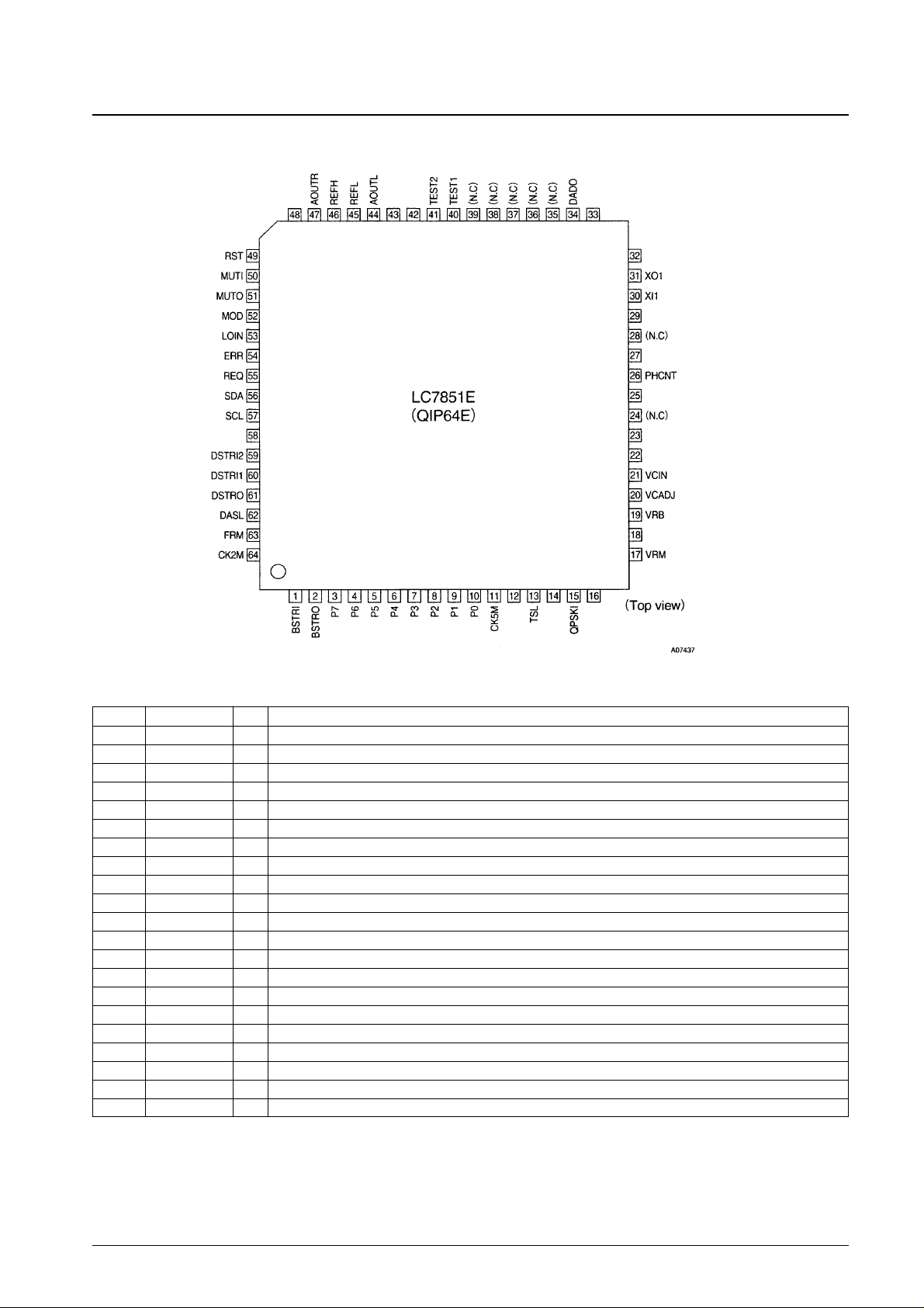
Pin Assignment
No. 5691-3/9
LC7851E
Pin Functions
Pin No. Pin I/O Function
1 BSTRI I Bit stream input
2 BSTRO O Bit stream output
3 P7 O General-purpose output port
4 P6 O General-purpose output port
5 P5 O General-purpose output port
6 P4 O General-purpose output port
7 P3 O General-purpose output port
8 P2 O General-purpose output port
9 P1 O General-purpose output port
10 P0 O General-purpose output port
11 CK5M O Filter adjustment clock output (5.7272 MHz)
12 DV
DD
I Digital system power supply
13 TSL I Output control for the state when reset by the PHCNT pin (Low: high-impedance, high: 50% duty pulse output)
14 AV
SS
I Internal A/D converter ground
15 QPSKI I QPSK modulated signal input
16 AV
DD
I Internal A/D converter power supply
17 VRM O Internal A/D converter reference (center) output
18 AV
SS
I Internal A/D converter ground
19 VRB O Internal A/D converter reference (low) output
20 VCADJ Connection for internal VCO adjustment external resistor
21 VCIN I Internal VCO control input
Continued on next page.
CV
DD
CV
SS
DV
SS
AV
DD
AV
SS
DV
DD
DV
SS
V
SS
V
DD
PV
SS
VV
SS
AV
SS
PV
DD
VV
DD
DV
DD
Page 4

No. 5691-4/9
LC7851E
Continued from preceding page.
Pin No. Pin I/O Function
22 VV
SS
I Internal VCO ground
23 VV
DD
I Internal VCO power supply
24 (N.C)
25 PV
DD
I Phase comparator power supply
26 PHCNT O Phase comparator output
27 PV
SS
I Phase comparator ground
28 (N.C)
29 V
DD
I Oscillator circuit power supply
30 XI1 I Crystal oscillator (22.909088 MHz) input
31 XO1 O Crystal oscillator (22.909088 MHz) output
32 V
SS
I Oscillator circuit ground
33 DV
SS
I Digital system ground
34 DADO O Digital audio interface output
35 (N.C)
36 (N.C)
37 (N.C)
38 (N.C)
39 (N.C)
40 TEST1 I Test pin
41 TEST2 I Test pin
42 DV
DD
I Digital system power supply
43 CV
SS
I Internal D/A converter ground
44 AOUTL O Left channel audio data output
45 REFL O Internal D/A converter reference voltage: low
46 REFH O Internal D/A converter reference voltage: high
47 AOUTR O Right channel audio data output
48 CV
DD
I Internal D/A converter power supply
49 RST I Reset input
50 MUTI I Forced muting input
51 MUTO O Mute detection output (When muting detected: high)
52 MOD O Audio mode detection output (A mode: low, B mode: high)
53 LOIN O Frame synchronization detection output (When synchronized: low)
54 ERR O Error detection output (Error detected: high)
55 REQ O Host CPU readout request signal
56 SDA I/O I
2
C bus data I/O
57 SCL I I
2
C bus clock input
58 DV
SS
I Digital system ground
59 DSTRI2 I Data stream input 2/general-purpose I/O port
60 DSTRI1 I Data stream input 1/general-purpose I/O port
61 DSTRO O Data stream output (post-error correction data)
62 DASL I Descrambler interface switching
63 FRM O Frame synchronization signal
64 CK2M O Bit stream clock (2.048 MHz)
Caution: All NC pins must be left open.
Page 5

Pin Input and Output Circuit Diagrams
• Output pins (Output pins other than P0 to P7, SDA, PHCNT, CK5M, VRM, VRB, REFH, REFL, AOUTR, and
AOUTL)
• Output pins: P0 to P7
• Output pin: CK5M
• Output pin: PHCNT
• Input pins: SCL, DSTRI1, and DSTRI2
• I/O pin: SDA
No. 5691-5/9
LC7851E
• Input pins (Input pins other than QPSKI, SCL, SDA, DSTRI1, DSTRI2, and VCIN)
These are n-channel open drain outputs.
Page 6

No. 5691-6/9
LC7851E
Parameter Symbol Conditions Ratings Unit
Supply voltage V
DD
–0.3 to +7.0 V
Input voltage V
I
1 Pins other than SCL and SDA –0.3 to VDD+0.3 V
V
I
2 SCL and SDA –0.3 to +5.3 V
Output voltage V
O
–0.3 to VDD +0.3 V
Allowable power dissipation Pd max Ta = –20 to +75°C 360 mW
Operating temperature Topr –20 to +75 °C
Storage temperature Tstg –40 to +125 °C
Specifications
Absolute Maximum Ratings at Ta = 25°C, VSS= 0 V
Parameter Symbol Conditions
Ratings
Unit
min typ max
Supply voltage V
DD
4.5 5.0 5.5 V
Input high-level voltage V
IH
0.75 V
DD
V
DD
V
Input low-level voltage V
IL
0 0.25 V
DD
V
QPSKI input voltage V
QPSKI
0.7 0.9 1.1 V
Allowable Operating Ranges at Ta = 25°C
Parameter Symbol Conditions
Ratings
Unit
min typ max
Current drain I
DD
68 98 mA
V
OH
= VDD– 0.4 V ; VOH= VDD– 0.4 V,
IOH1
CMOS output pins:PHCNT, LOIN, MOD,
1.0 mA
DSTRO, FRM, ERR, CK2M, BSTRO, MUTO,
Output high-level current
DADO, REQ, SYCKO
I
OH
2 VOH= V
CK5MH
– 25 mV, CK5M –350 –100 µA
V
OL
= 0.4 V ; CMOS output pins: PHCNT,
I
OL
1 LOIN, MOD, DSTRO, FRM, ERR, CK2M, 1.0 mA
BSTRO, MUTO, DADO, REQ, SYCKO
I
OL
2
V
OL
= 0.4 V, open drain output
1.0 mA
Output low-level current 1 Pin 1: P0 to P7
I
OL
3
V
OL
= 0.4 V, open drain output
4.0 mA
Pin 2: SDA
I
OL
4 VOL= V
CK5ML
+ 25 mV, CK5M 100 350 µA
Output amplitude level V
CK5MIOH
= 30 µA, CK5M 236 295 354 mV
V
I
= VDD, Schmitt inputs: TSL, RST, TEST1,
Input high-level current I
IH
TEST2, BSTRI, DSTRI1, DSTRI2, DASL, 10 µA
MUTI, SCL, SDA, P0 to P7
VI= VSS, Schmitt inputs: TSL, RST, TEST1,
Input low-level current I
IL
TEST2, BSTRI, DSTRI1, DSTRI2, DASL, –10 µA
MUTI, SCL, SDA, P0 to P7
Output load resistance R
L
AOUTL and AOUTR 5.0 kΩ
DC Characteristics at Ta = –20 to +75°C, VDD= 4.5 to 5.5 V, GND = 0 V
Parameter Symbol Conditions
Ratings
Unit
min typ max
Resolution RES 1 kHz 0 dB 16 Bits
Total harmonic distortion
THD1 1 kHz A mode, FS - 18 dB * 0.08 %
THD2 1 kHz B mode, FS - 18 dB * 0.05 %
Signal-to-noise ratio S/N 1 kHz 0 dB * 105 dB
Crosstalk C. T 1 kHz 0 dB * 95 dB
Full scale output voltage VFS 2.8 3.0 3.2 Vp-p
D/A Converter Characteristics at Ta = –20 to +75°C, VDD= 4.5 to 5.5 V, GND = 0 V
Note: *Values when measured in the Sanyo evaluation board and with a QPSK modulated signal (1 kHz sine wave) input.
Page 7

No. 5691-7/9
LC7851E
Parameter Symbol Conditions
Ratings
Unit
min typ max
SCL frequency f
SCL
100 kHz
Bus release time T
BUF
4.7 µs
Start hold time T
HD STA
4.0 µs
SCL low time T
LOW
4.7 µs
SCL high time T
HIGH
4.0 µs
Data hold time T
HD DAT
0 ns
Data setup time T
SU DAT
250 ns
Rise time T
R
1000 ns
Fall time T
F
300 ns
Stop setup time T
SU STO
4.0 µs
I2C Bus Interface at Ta = –20 to +75°C, VDD= 4.5 to 5.5 V, GND = 0 V
S: Start condition
P: Stop condition
Parameter Symbol Conditions
Ratings
Unit
min typ max
Clock pulse width T
CK2M
244 ns
BSTRO pin output delay time T
BSDL
15 ns
DSTRO pin output delay time T
DSDL
15 ns
BSTRI and DSTRI1 two-pin input setup time T
BSST
10 ns
Descrambler Interface at Ta = –20 to +75°C, VDD= 4.5 to 5.5 V, GND = 0 V
Parameter Symbol Conditions
Ratings
Unit
min typ max
Reset time T
RST
TSL pin high; The LC7851E must be used
200 ms
with the TSL pin (pin 13) high.
The LC7851E must be reset with the following timing when power is first applied.
Reset Timing at Power on at Ta = –20 to +75°C, VDD= 4.5 to 5.5 V, GND = 0 V
Recommended Crystal Oscillator Constants
Pin I/O Circuit
Supplier Oscillator element Cin/Cout
Citizen Watch Co., Ltd.
CSA-309 5pF
(22.909088 MHz) (Cin = Cout)
Pin 30
Pin 31
Page 8

Application Circuit Diagram
No. 5691-8/9
LC7851E
Page 9

No. 5691-9/9
LC7851E
This catalog provides information as of August, 1997. Specifications and information herein are subject to
change without notice.
■ No products described or contained herein are intended for use in surgical implants, life-support systems, aerospace
equipment, nuclear power control systems, vehicles, disaster/crime-prevention equipment and the like, the failure of
which may directly or indirectly cause injury, death or property loss.
■ Anyone purchasing any products described or contained herein for an above-mentioned use shall:
➀ Accept full responsibility and indemnify and defend SANYO ELECTRIC CO., LTD., its affiliates, subsidiaries and
distributors and all their officers and employees, jointly and severally, against any and all claims and litigation and all
damages, cost and expenses associated with such use:
➁ Not impose any responsibility for any fault or negligence which may be cited in any such claim or litigation on
SANYO ELECTRIC CO., LTD., its affiliates, subsidiaries and distributors or any of their officers and employees
jointly or severally.
■ Information (including circuit diagrams and circuit parameters) herein is for example only; it is not guaranteed for
volume production. SANYO believes information herein is accurate and reliable, but no guarantees are made or implied
regarding its use or any infringements of intellectual property rights or other rights of third parties.
 Loading...