

Page 1

Applications
Function switching under serial data control in amplifiers,
receivers, and other electronic equipment
Features
• Two sets of eight (or in the LC78213, seven) built-in
circuits with three switching configurations available
based on differing internal connections
• Control according to serial data sent from a microprocessor, and easy connection to 5 V microprocessors
• Two identical products can be connected to a shared bus
due to the provision of a select pin (S).
• A reset pin that turns off all analog switches
• A ±20 V withstand voltage rating allows these products
to provide a wide dynamic range.
Package Dimensions
unit: mm
3061-DIP30S
CMOS LSI
Ordering number : EN4817A
73096HA (OT)/72994 TH (OT) No. 4817-1/6
SANYO: DIP30S
[LC78211, 78212, 78213]
SANYO Electric Co.,Ltd. Semiconductor Bussiness Headquarters
TOKYO OFFICE Tokyo Bldg., 1-10, 1 Chome, Ueno, Taito-ku, TOKYO, 110 JAPAN
Analog Function Switch
LC78211, 78212, 78213
Specifications
Absolute Maximum Ratings at Ta = 25°C
Parameter Symbol Conditions Ratings Unit
Maximum supply voltage
V
DD
max V
DD
–0.3 to +20 V
V
EE
max V
EE
–20 to +0.3 V
Maximum input voltage
V
I
1 DI, CL, CE, S, RES –0.3 to +20 V
V
I
2 L1 to L8, R1 to R8, LCOM1 to LCOM4, RCOM1 to RCOM4 VEE– 0.3 to VDD+ 0.3 V
Analog switch potential difference when on ∆V
ON
With the switch on 0.5 V
Allowable power dissipation Pd max Ta ≤ 75°C 100 mW
Operating temperature range Topr –30 to +75 °C
Storage temperature range Tstg –40 to +125 °C
Page 2
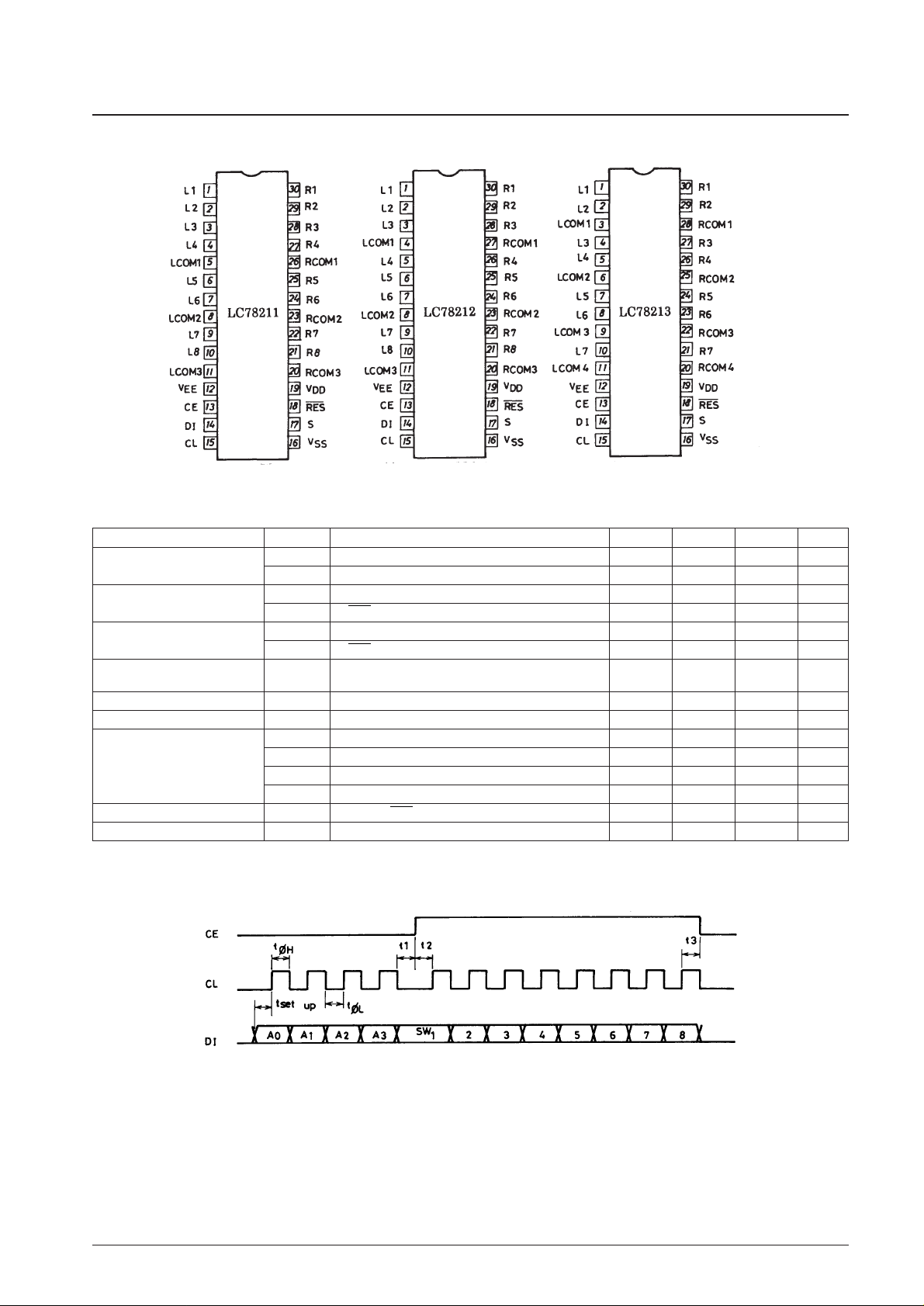
Pin Assignments
Allowable Operating Ranges at Ta = 25°C, VSS= 0 V, | VDD| ≥ | VEE|
Note: * CE, CL and DI waveforms
No. 4817-2/6
LC78211, 78212, 78213
Parameter Symbol Conditions min typ max Unit
Maximum supply voltage
V
DD
VDD– VEE≥ 12 V: V
DD
6.0 18.5 V
V
EE
VDD– VEE≥ 12 V: V
EE
–18.5 0 V
Input high level voltage
V
IH
1 DI, CL, CE 4.0 18.5 V
V
IH
2 S, RES 0.7 V
DD
V
DD
V
Input low level voltage
V
IL
1 DI, CL, CE 0 0.7 V
V
IL
2 S, RES 0 0.3 V
DD
V
Analog switch input
V
IN
L1 to L8, R1 to R8, LCOM1 to LCOM4,
V
EE
V
DD
V
voltage range RCOM1 to RCOM4
Low level clock pulse width t
øL
CL 0.5 µs
High level clock pulse width t
øH
CL 0.5 µs
t
set up
CL, DI 0.5 µs
Setup time
t1* CL, CE 0.5 µs
t2* CL, CE 0.5 µs
t3* CL, CE 0.5 µs
Minimum reset pulse width t
wRESVDD
≥ 6 V: RES 1.0 µs
Hysteresis V
H
CL, CE, DI 0.3 V
Top view
Page 3

Electrical Characteristics at Ta = 25°C, VSS= 0 V
Equivalent Circuit Block Diagrams
No. 4817-3/6
LC78211, 78212, 78213
Parameter Symbol Conditions min typ max Unit
I = 1 mA, V
DD
– VEE= 12 V:
R
ON
1 L1 to L8, R1 to R8, LCOM1 to LCOM4, 150 Ω
Analog switch on resistance
RCOM1 to RCOM4
I = 1 mA, VDD– VEE= 37 V:
R
ON
2 L1 to L8, R1 to R8, LCOM1 to LCOM4, 70 Ω
RCOM1 to RCOM4
VIN= 1 Vrms, f = 1 kHz, VDD– VEE= 37 V:
THD1 L1 to L8, R1 to R8, LCOM1 to LCOM4, 0.0015 0.01 %
Total harmonic distortion
RCOM1 to RCOM4
V
IN
= 0.1 Vrms, f = 1 kHz, VDD– VEE= 37 V:
THD2 L1 to L8, R1 to R8, LCOM1 to LCOM4, 0.01 0.05 %
RCOM1 to RCOM4
V
IN
= 0 dBV, f = 10 kHz, VDD– VEE= 37 V:
Feedthrough F
TH
L1 to L8, R1 to R8, LCOM1 to LCOM4, 55 dB
RCOM1 to RCOM4
VIN= 0 dBV, f = 10 kHz, VDD– VEE= 37 V:
Crosstalk CT L1 to L8, R1 to R8, LCOM1 to LCOM4, 75 dB
RCOM1 to RCOM4
Input high level current I
IH
VI= 18.5 V: DI, CL, CE, S, RES +10 µA
Input low level current I
IL
VI= 0 V: DI, CL, CE, S, RES –10 µA
Analog switch leakage current
V
I
= VEEto VEE+ 37 V:
(off state)
I
OFF
L1 to L8, R1 to R8, LCOM1 to LCOM4, –10 +10 µA
RCOM1 to RCOM4
Current drain I
DD
V
DD
1.0 mA
Continued on next page.
Page 4

Continued from preceding page.
No. 4817-4/6
LC78211, 78212, 78213
Page 5

Pin Functions
Operation
1. Data Input Procedure
The LC78211, LC78212 and LC78213 are controlled by inputting specified data to the CL, DI and CE pins. The
input data consists of 12 bits, of which four bits are address and eight bits are data.
Bits correspond to the L1 to L8 and R1 to R8 analog switches, and a value of one turns the corresponding switch on,
and a value of zero turns it off.
0.........Off
1.........On
The address is used when the chip is connected to a shared bus. The data (address) that must be transmitted depends
on the S pin and the particular product as shown in the table below.
Note: The bit for switch eight in the LC78213 is a “don’t care” bit, that is it can be either 0 or 1 without affecting
chip function. This is because the LC78213 has two sets of seven (not eight) circuits.
No. 4817-5/6
LC78211, 78212, 78213
Pin I/O Internal equivalent circuit Pin function
VDD, VSS, V
EE
L1 to L8, R1 to R8,
LCOM1 to LCOM4,
RCOM1 to RCOM4
CL, DI, CE
S
RES
I
I
I
See the block diagram.
Power supply
Analog switch input and output
Serial data input (Schmitt buffer)
CL..............Clock input
DI...............Data input
CE .............Chip enable
Selection of one of two chips
The address is set to the values shown in the table below according to
the level input to the S pin.
Reset input
The states of the analog switches are undefined when power is first
applied. Setting this pin low will force all switches the off state.
Product
S pin
Address
level
A
0
A
1
A
2
A
3
LC78211
L 0 1 0 1
H 1 1 0 1
LC78212
L 0 0 1 1
H 1 0 1 1
LC78213
L 0 1 1 1
H 1 1 1 1
Product
S pin
Address
level
A
0
A
1
A
2
A
3
LC78211
L 0 1 0 1
H 1 1 0 1
LC78212
L 0 0 1 1
H 1 0 1 1
LC78213
L 0 1 1 1
H 1 1 1 1
Page 6

No. 4817-6/6
LC78211, 78212, 78213
2. DI, CL and CE Timing
Data is read in on the rising edge of CL and latched on the falling edge of CE.
3. Notes on the Reset Pin
The states of the analog switches are undefined when power is first applied. However, it is possible to use the reset
pin to force all switches to the off state by connecting an RC circuit to this pin.
4. Using a CCB Bus with Multiple ICs
The LC78211, LC78212 and LC78213 retain their prior state until they receive data with a matching address.
5. Replacing Earlier Models
Caution is required when replacing an LC7821N, LC7823N and LC7823N with an LC78211, LC78212 and
LC78213, since the S pin threshold levels differ.
6. Handling of Unused Input Pins
We recommend connecting any unused switch pin to VSSthrough a resistor of up to a few 100 kΩ to prevent damage
from static electricity.
This catalog provides information as of July, 1996. Specifications and information herein are subject to change
without notice.
■ No products described or contained herein are intended for use in surgical implants, life-support systems, aerospace
equipment, nuclear power control systems, vehicles, disaster/crime-prevention equipment and the like, the failure of
which may directly or indirectly cause injury, death or property loss.
■ Anyone purchasing any products described or contained herein for an above-mentioned use shall:
① Accept full responsibility and indemnify and defend SANYO ELECTRIC CO., LTD., its affiliates, subsidiaries and
distributors and all their officers and employees, jointly and severally, against any and all claims and litigation and all
damages, cost and expenses associated with such use:
➁ Not impose any responsibility for any fault or negligence which may be cited in any such claim or litigation on
SANYO ELECTRIC CO., LTD., its affiliates, subsidiaries and distributors or any of their officers and employees
jointly or severally.
■ Information (including circuit diagrams and circuit parameters) herein is for example only; it is not guaranteed for
volume production. SANYO believes information herein is accurate and reliable, but no guarantees are made or implied
regarding its use or any infringements of intellectual property rights or other rights of third parties.
 Loading...