

Page 1
Overview
The LC78011E is a CMOS IC that integrates a digital
RGB encoder and a synchronizing signal generation
circuit on a single chip. A video CD or CD-G system can
be formed using the LC78011E together with an MPEG
video decoder or a CD-G decoder, respectively.
Features
• System structure
— Each system (Video CD or CD-G system) formed
with an additional chip: MPEG decoder or CD-G
decoder chip.
• Video outputs
— 8-bit D/A converter outputs: 2 channels
— The LC78011E supports the following two video
signal output formats:
Luminance signal (Y) and chroma signal (C) outputs
Composite video signal (C • VIDEO) output (Only
one D/A converter channel operates in this mode.)
• System clock
— External 4fsc clock
NTSC mode: 14.31818 MHz
PAL mode: 17.734475 MHz
PAL-M mode: 14.30244596 MHz
• External subcarrier input
— An external fsc clock is input and used for subcarrier
synchronization timing.
• Video data input
— The LC78011E supports the following four input
formats:
R, G, and B: 8 bits each
Y, U, and V: 8 bits each
Y and UV: 8 bits each (The UV input is a
multiplexed input)
R, G, and B: 4 bits each (In CD-G input support
mode)
• OSD input support
— R, G, and B + BLK 4-bit inputs (color support)
(BLK is an OSD display switching timing signal.)
• External synchronizing signal input
— Horizontal synchronizing signal, composite
synchronizing signal, and composite blanking signal
inputs: HSYNC, CSYNC, and BLANK.
• Video signal formats
— The LC78011E supports the NTSC, PAL, and PAL-
M formats.
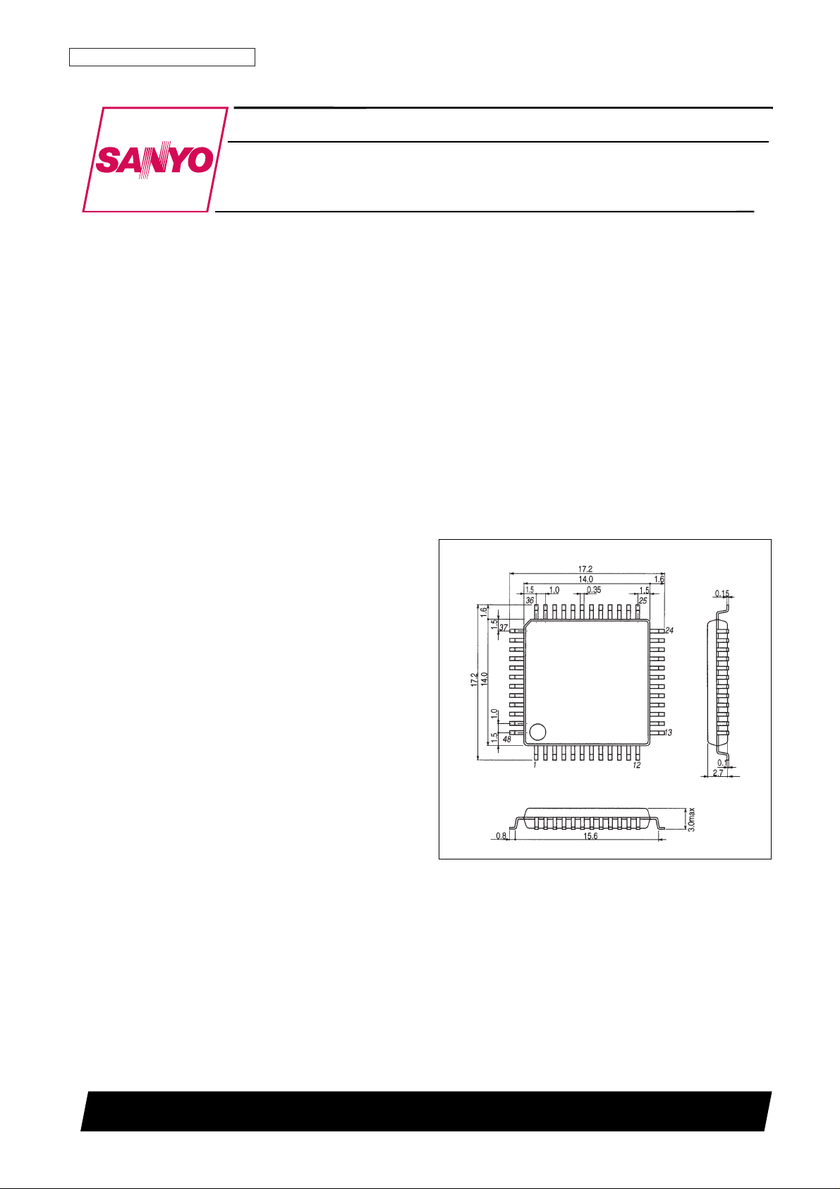
Package Dimensions
unit: mm
3156-QIP48E
CMOS IC
33198RM (OT) No. 5755-1/13
SANYO: QIP48E
[LC78011E]
SANYO Electric Co.,Ltd. Semiconductor Bussiness Headquarters
TOKYO OFFICE Tokyo Bldg., 1-10, 1 Chome, Ueno, Taito-ku, TOKYO, 110-8534 JAPAN
Digital RGB Encoder IC for Video CD and CD-G
LC78011E
Ordering number : EN5755
Page 2

Pin Assignment
No. 5755-2/13
LC78011E
Page 3
No. 5755-3/13
LC78011E
Pin Functions
Pin No. Symbol I/O Polarity Function
1 RYIN3 IN Positive R/Y data input A pull-down resistor is built in.
2 RYIN2 IN Positive R/Y data input A pull-down resistor is built in.
3 RYIN1 IN Positive R/Y data input A pull-down resistor is built in.
4 RYIN0 IN Positive R/Y data input (LSB) A pull-down resistor is built in.
5 DV
SS
— — Digital system ground
6 CLKI IN — 4fsc clock input A feedback resistor is built in.
7 FSCIN IN — fsc clock input A feedback resistor is built in.
8 DV
DD
— — Digital system power supply
9 GUIN7 IN Positive G/U data input (MSB) A pull-down resistor is built in.
10 GUIN6 IN Positive G/U data input A pull-down resistor is built in.
11 GUIN5 IN Positive G/U data input A pull-down resistor is built in.
12 GUIN4 IN Positive G/U data input A pull-down resistor is built in.
13 GUIN3 IN Positive G/U data input A pull-down resistor is built in.
14 GUIN2 IN Positive G/U data input A pull-down resistor is built in.
15 GUIN1 IN Positive G/U data input A pull-down resistor is built in.
16 GUIN0 IN Positive G/U data input (LSB) A pull-down resistor is built in.
17 BVIN7 IN Positive B/V/UV data input (MSB) A pull-down resistor is built in.
18 BVIN6 IN Positive B/V/UV data input A pull-down resistor is built in.
19 BVIN5 IN Positive B/V/UV data input A pull-down resistor is built in.
20 BVIN4 IN Positive B/V/UV data input A pull-down resistor is built in.
21 BVIN3 IN Positive B/V/UV data input A pull-down resistor is built in.
22 BVIN2 IN Positive B/V/UV data input A pull-down resistor is built in.
23 BVIN1 IN Positive B/V/UV data input A pull-down resistor is built in.
24 BVIN0 IN Positive B/V/UV data input (LSB) A pull-down resistor is built in.
25 AV
DD
— — Analog system power supply (For the D/A converters.) (+5 V)
26 CROUT OUT — Chroma signal/composite video signal output (8-bit D/A converter output)
27 BIAS OUT — Ripple rejection capacitor connection (Use a 10 µF capacitor.)
28 YOUT OUT — Luminance signal output (8-bit D/A converter output)
29 AV
SS
— — Analog system ground (For the D/A converters.)
30 CCSEL IN Positive D/A converter output control signal input (Low: YC signal output, High: Composite video signal output)
31 NPSEL IN Positive Signal format selection input
32 PMSEL IN Positive
33 CDGSEL IN Negative
Video CD/CD-G selection input (Low: CD-G, High: Video-CD)
(The input digital data can be selected to be either 4-bit or 8-bit data.)
34 TEST IN Positive Test mode selection input (This pin must be tied low during normal operation.)
35 RESET IN Negative Reset signal input
36 OSBIN IN Positive OSD signal (B) input
37 OSGIN IN Positive OSD signal (G) input
38 OSRIN IN Positive OSD signal (R) input
39 OSBLK IN Positive OSD switching signal input (The OSD blanking signal input)
NPSEL PMSEL D/A converter output signal mode
0 0 NTSC
1 0 PAL
0 1 PAL-M
1 1 – (Illegal setting)
Continued on next page.
Page 4
No. 5755-4/13
LC78011E
Continued from preceding page.
Pin No. Symbol I/O Polarity Function
40 BLANK IN Positive Composite blanking signal input (HBLANK + VBLANK)
41 CSYNC IN Negative Composite synchronizing signal input (HSYNC + VSYNC)
42 HSYNC IN Negative Horizontal synchronizing signal input (HSYNC)
43 YUVSEL1 IN Positive Signal input setup
44 YUVSEL2 IN Positive
45 RYIN7 IN Positive R/Y data input (MSB) A pull-down resistor is built in.
46 RYIN6 IN Positive R/Y data input A pull-down resistor is built in.
47 RYIN5 IN Positive R/Y data input A pull-down resistor is built in.
48 RYIN4 IN Positive R/Y data input A pull-down resistor is built in.
YUVSEL1 YUVSEL2 Video signal input signal mode
0 0 RYIN = R in, GUIN = G in, BVIN = B in
1 0 RYIN = Y in, GUIN = U in, BVIN = V in
0 1 RYIN = Y in, GUIN = none, BVIN = UV in
1 1 — (Illegal setting)
Notes:1. The voltage applied as the digital system power supply voltage must not exceed the voltage applied as the analog system power supply voltage.
2. Unused input pins must be tied high or low. If the OSD inputs are not used, tie OSBLK (pin 39) low.
3. Note that the clock input frequencies (CLKI: pin 6, and FSCIN: pin 7) depend on the TV subcarrier pull-in range. The CLKI input clock and the
FSCIN clock must be synchronized.
Parameter Symbol Conditions Ratings Unit
Maximum supply voltage
V
DD
1 max DVDD(DVDD≤ AVDD) DVSS– 0.3 to DVSS+7.0 V
V
DD
2 max AV
DD
AVSS– 0.3 to AVSS+7.0 V
RYIN0 to RYIN7, GUIN0 to GUIN7,
BVIN0 to BVIN7, CLKI, FSCIN,
Input voltage V
IN
OSRIN, OSGIN, OSBIN, OSBLK,
DV
SS
– 0.3 to DVDD+0.3 V
BLANK, CSYNC, HSYNC, RESET,
CCSEL, NPSEL, PMSEL, CDGSEL,
YUVSEL1, YUVSEL2, and TEST
Output voltage V
OUT
CROUT, YOUT, and BIAS DVSS– 0.3 to DVDD+0.3 V
Allowable power dissipation Pd max Ta = 25°C 500 mW
Operating temperature Topr –20 to +75 °C
Storage temperature Tstg –40 to +125 °C
Specifications
Absolute Maximum Ratings
Parameter Symbol Conditions
Ratings
Unit
min typ max
Supply voltage
V
DD
1 DVDD(DVDD≤ AVDD) 3.0 5.5 V
V
DD
2 AV
DD
4.5 5.0 5.5 V
OSRIN, OSGIN, OSBIN, OSBLK
VIH1 CCSEL, NPSEL, PMSEL, CDGSEL, 0.7 VDD1 VDD1 + 0.3 V
Input high-level voltage
YUVSEL1, YUVSEL2, TEST
RYIN0 to RYIN7, GUIN0 to GUIN7,
V
IH
2 BVIN0 to BVIN7, BLANK, CSYNC 2.2 VDD1 + 0.3 V
HSYNC, RESET
OSRIN, OSGIN, OSBIN, OSBLK
V
IL
1 CCSEL, NPSEL, PMSEL, CDGSEL, VSS1 – 0.3 0.3 VDD1 V
Input low-level voltage
YUVSEL1, YUVSEL2, TEST
RYIN0 to RYIN7, GUIN0 to GUIN7,
V
IL
2 BVIN0 to BVIN7, BLANK, CSYNC VSS1 – 0.3 0.8 V
HSYNC, RESET
NTSC 14.31818 MHz
f
IN
1 CLKI PAL 17.734475 MHz
Clock frequency
PAL-M 14.3024459 MHz
NTSC 3.579545 MHz
f
IN
2 FSCIN PAL 4.43361875 MHz
PAL-M 3.57561149 MHz
Allowable Operating Ranges at Ta = –20 to 75°C unless otherwise specified
Continued on next page.
Page 5

No. 5755-5/13
LC78011E
Continued from preceding page.
Parameter Symbol Conditions
Ratings
Unit
min typ max
Input amplitude
V
IN
1 CLKI (capacitor coupled) 2.0 VDD1 Vp-p
V
IN
2 FSCIN (capacitor coupled) 2.0 VDD1 Vp-p
Clock duty Fduty1 CLKI, FSCIN 40 50 60 %
Reset pulse width t
wrst
RESET 400 ns
Parameter Symbol Conditions
Ratings
Unit
min typ max
OSRIN, OSGIN, OSBIN, OSBLK,
I
IH
1
BLANK, CSYNC, HSYNC, RESET, 5 µA
CCSEL, NPSEL, PMSEL, CDGSEL,
Input high-level current
YUVSEL1, YUVSEL2, TEST: V
IN
= DV
DD
RYIN0 to RYIN7, GUIN0 to GUIN7,
I
IH
2 BVIN0 to BVIN7 (Pull-down resistors 25 50 75 µA
are built in): V
IN
= DV
DD
OSRIN, OSGIN, OSBIN, OSBLK,
IIL1
BLANK, CSYNC, HSYNC, RESET, –5 µA
CCSEL, NPSEL, PMSEL, CDGSEL,
Input low-level current
YUVSEL1, YUVSEL2, TEST: V
IN
= DV
SS
RYIN0 to RYIN7, GUIN0 to GUIN7,
I
IL
2 BVIN0 to BVIN7 (Pull-down resistors –5 µA
are built in): V
IN
= DV
SS
Internal feedback resistance R
BIAS
CLKI, FSCIN 1 MΩ
D/A converter resolution YOUT, CROUT 8 bits
D/A converter output resistance R
DAC
YOUT, CROUT 150 300 500 Ω
YOUT, CROUT
D/A converter reference voltage V
REF
(The output voltage when each bit of the 8-bit 2.40 2.45 2.50 V
data is zero)
(DVDD= 5.0 V : NTSC) 37 56 mA
IDD1
DV
DD
(DVDD= 5.0 V : PAL) 45 68 mA
(AV
DD
= 5.0 V) (DVDD= 3.3 V : NTSC) 15 23 mA
(DV
DD
= 3.3 V : PAL) 18 27 mA
(DV
DD
= 5.0 V : When 2
21 37 mA
Operating current drain channels are used)
(DV
DD
= 5.0 V : When 1
12 21 mA
I
DD
2
AV
DD
channel is used)
(AV
DD
= 5.0 V) (DVDD= 3.3 V :When 2
22 39 mA
channels are used)
(DV
DD
= 3.3 V : When 1
13 23 mA
channel is used)
Electrical Characteristics at Ta = –20 to 75°C, DVDD= 5.0 V, AVDD= 5.0 V unless otherwise specified
Parameter Symbol Conditions
Ratings
Unit
min typ max
RYIN0 to 7, GUIN0 to 7, BVIN0 to 7
→ CLKI
BLANK, CSYNC, HSYNC → CLKI
Data setup time t
DS
OSRIN, OSGIN, OSBIN, OSBLK → CLKI
FSCIN → CLKI
: DV
DD
= 5.0 V 0 ns
: DV
DD
= 3.3 V 0 ns
CLKI → RYIN0 to 7, GUIN0 to 7, BVIN0 to 7
CLKI → BLANK, CSYNC, HSYNC
Data hold time t
DH
CLK → OSRIN, OSGIN, OSBIN, OSBLK
CLKI → FSCIN
: DV
DD
= 5.0 V 10 ns
: DV
DD
= 3.3 V 12 ns
Minimum clock pulse width
t
WL
CLKI (For a square wave input) 18 ns
t
WH
CLKI (For a square wave input) 18 ns
Input clock duty tduty CLKI, FSCIN (For a sine wave input) 40 60 %
Timing Characteristics at Ta = 25°C, DVDD= 5.0 V, AVDD= 5.0 V, tr= tf= 3 ns unless otherwise specified
Page 6

Timing Charts
Data Input
No. 5755-6/13
LC78011E
Synchronizing Signal Input
Subcarrier Input
OSD Input
Page 7

Composite Video Signal (C • VIDEO) Output
No. 5755-7/13
LC78011E
Note: The value in parentheses is the burst amplitude for PAL and PAL-M modes.
Digital value (8 bits)
Sync tip Burst
White
Yellow
Cyan
Green
Magenta
Red
Blue
Black
Frame
Character
Frame
Black
Page 8

No. 5755-8/13
LC78011E
Luminance Signal Output (Y)
Sync tip Burst
White
Yellow
Cyan
Green
Magenta
Red
Blue
Black
Frame
Character
Frame
Black
Digital value (8 bits)
Page 9

No. 5755-9/13
LC78011E
Chroma Signal (C) Output
Note: The value in parentheses is the burst amplitude for PAL and PAL-M modes.
Digital value (8 bits)
Burst
White
Yellow
Cyan
Green
Magenta
Red Blue
Black
Page 10

System Block Diagram
No. 5755-10/13
LC78011E
(Luminance signal output)
(Chroma signal or composite
video signal output)
Luminance signal
(Y) processing
circuit
Chroma signal (C)
processing circuit
Timing generator
OSD signal
insertion circuit
Matrix circuit
Burst signal
generator
YUV to RGB converter
Buffer circuit
System clock
Page 11

Functional Description
1. Clocks
The system clock operates at 4fsc and is input to the CLKI pin (pin 6). A feedback (bias) resistor is built in.
Input clock frequencies:
NTSC mode: 14.31818 MHz
PAL mode: 17.734475 MHz
PAL-M mode: 14.30244596 MHz
2. Video signal output formats
The LC78011E can provide either a Y/C (luminance signal/chrominance signal) separated signal output or a
composite video signal output.
The CCSEL pin (pin 30) selects the output format.
3. Digital video input switching
The LC78011E supports both input from an MPEG decoder (24 bits, 8 bits each of R, G, and B data) and a 12-bit
CD-G input (4 bits each of R, G, and B data). The CDGSEL pin (pin 33) switches the input.
• Sample CD-G (LC7874E) connection
4. Digital video input format selection
The LC78011E supports both RGB and YUV formats. The YUVSEL1 and YUVSEL2 pins (pins 43 and 44) are
used to select the input video format.
No. 5755-11/13
LC78011E
CCSEL (pin 30) setting High = 1 Low = 0
CROUT (pin 26) output Composite video signal Chroma signal (C)
YOUT (pin 28) output
Fixed low-level output
Luminance signal (Y)
(The D/A converter is stopped.)
CDGSEL (pin 33) Low = 0 High = 1
Digital input selection 12-bit input (CD-G) 24-bit input (Video CD)
LC78011E LC7874E
RYIN7 (pin 45) ROUT3 (pin 36)
R
RYIN6 (pin 46) ROUT2 (pin 37)
RYIN5 (pin 47) ROUT1 (pin 38)
RYIN4 (pin 48) ROUT0 (pin 39)
GUIN7 (pin 9) GOUT3 (pin 42)
G
GUIN6 (pin 10) GOUT2 (pin 43)
GUIN5 (pin 11) GOUT1 (pin 44)
GUIN4 (pin 12) GOUT0 (pin 45)
BVIN7 (pin 17) BOUT3 (pin 46)
B
BVIN6 (pin 18) BOUT2 (pin 47)
BVIN5 (pin 19) BOUT1 (pin 48)
BVIN4 (pin 20) BOUT0 (pin 49)
YUVSEL2 (pin 44) YUVSEL1 (pin 43) Input format
Low = 0 Low = 0 RGB input
Low = 0 High = 1 YUV input
High = 1 Low = 0 Y/UV input*
High = 1 High = 1 Illegal value
Note :* GUIN0 to GUIN7 are not used in the Y/UV input mode.
The U/V discrimination for the UV input is performed by starting acquisition of the U input data with a timing referenced to the falling edge of
the BLANK pin (pin 40) input signal. In this mode, the input pins GUIN0 to GUIN7 must be left open or tied to DVSS. (These inputs include
built-in pull-down resistors.)
Page 12

• Data input timing
RGB input (24 bits) YCbCr (YUV) input (24 bits)
Y (8 bits), CbCr (8 bits) multiplexed input
5. OSD input (on-screen display data input)
The LC78011E provides an OSD signal RGB input function. Four input signals are required: the 3 bits of R, G, and B
data and the BLANK pin input signal, which is used for OSD switching.
Note: The white luminance level is 162, and the black and framing luminance level is 66. (When converted from the As 8-bit data values.)
• OSD timing
When no framing is used When a frame is used (Frame color: black)
6. Signal format switching (NTSC, PAL, or PAL-M)
The NPSEL and PMSEL pin (pin 31 and 32) are used to switch the signal format.
No. 5755-12/13
LC78011E
R (OSRIN: pin 38) G (OSGIN: pin 37) B (OSBIN: pin 36) OSBLK (pin 39) OSD display color
L = 0 L = 0 L = 0 L = 0 Display off
L = 0 L = 0 L = 0 H = 1 Black
H = 1 L = 0 L = 0 H = 1 Red
L = 0 H = 1 L = 0 H = 1 Green
L = 0 L = 0 H = 1 H = 1 Blue
H = 1 L = 0 H = 1 H = 1 Magenta
H = 1 H = 1 L = 0 H = 1 Yellow
L = 0 H = 1 H = 1 H = 1 Cyan
H = 1 H = 1 H = 1 H = 1 White
NPSEL (pin 31) PMSEL (pin 32) Signal format
L = 0 L = 0 NTSC
H = 1 L = 0 PAL
L = 0 H = 1 PAL-M
H = 1 H = 1 Illegal value
Character
Character
Frame
Frame
Page 13

PS No. 5755-13/13
LC78011E
This catalog provides information as of March, 1998. Specifications and information herein are subject to
change without notice.
■ No products described or contained herein are intended for use in surgical implants, life-support systems, aerospace
equipment, nuclear power control systems, vehicles, disaster/crime-prevention equipment and the like, the failure of
which may directly or indirectly cause injury, death or property loss.
■ Anyone purchasing any products described or contained herein for an above-mentioned use shall:
➀ Accept full responsibility and indemnify and defend SANYO ELECTRIC CO., LTD., its affiliates, subsidiaries and
distributors and all their officers and employees, jointly and severally, against any and all claims and litigation and all
damages, cost and expenses associated with such use:
➁ Not impose any responsibility for any fault or negligence which may be cited in any such claim or litigation on
SANYO ELECTRIC CO., LTD., its affiliates, subsidiaries and distributors or any of their officers and employees
jointly or severally.
■ Information (including circuit diagrams and circuit parameters) herein is for example only; it is not guaranteed for
volume production. SANYO believes information herein is accurate and reliable, but no guarantees are made or implied
regarding its use or any infringements of intellectual property rights or other rights of third parties.
 Loading...