

Page 1
Ordering number : ENN*6473
41000RM (OT) No. 6473 -1/33
Overview
The LC75878E and LC75878W are 1/8 to 1/10 duty
general-purpose LCD display drivers used for character
and graphics display. These products operate under the
control of a microcontroller and can directly drive an LCD
with up to 730 segments. They can also control up to 4
general-purpose output ports.
Features
• 1/8duty–1/4bias, 1/9duty–1/4bias, and 1/10duty–1/4bias
drive schemes can be controlled from serial data.
1/8duty–1/4bias: up to 600 segments
1/9duty–1/4bias: up to 666 segments
1/10duty–1/4bias: up to 730 segments
• Serial data input supports CCB format communication
with the system controller.
• Serial data control of the power-saving mode based
backup function and all the segments forced off
function.
• Direct display of display data without the use of a
decoder provides high generality.
• Built-in display contrast adjustment circuit.
• Up to 4 general-purpose output ports are included.
• Independent LCD driver block power supply V
LCD
.
• The INH pin is provided. This pin turns off the display
and forces the general-purpose output ports to the low
level.
• RC oscillator circuit
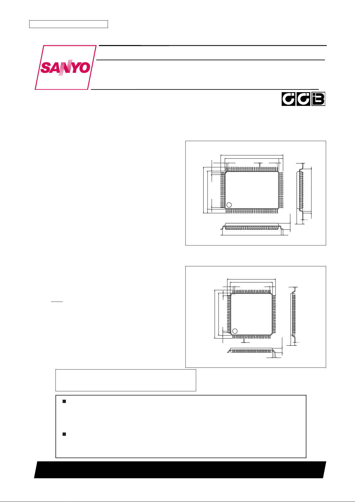
Package Dimensions
unit: mm
3151-QFP100E
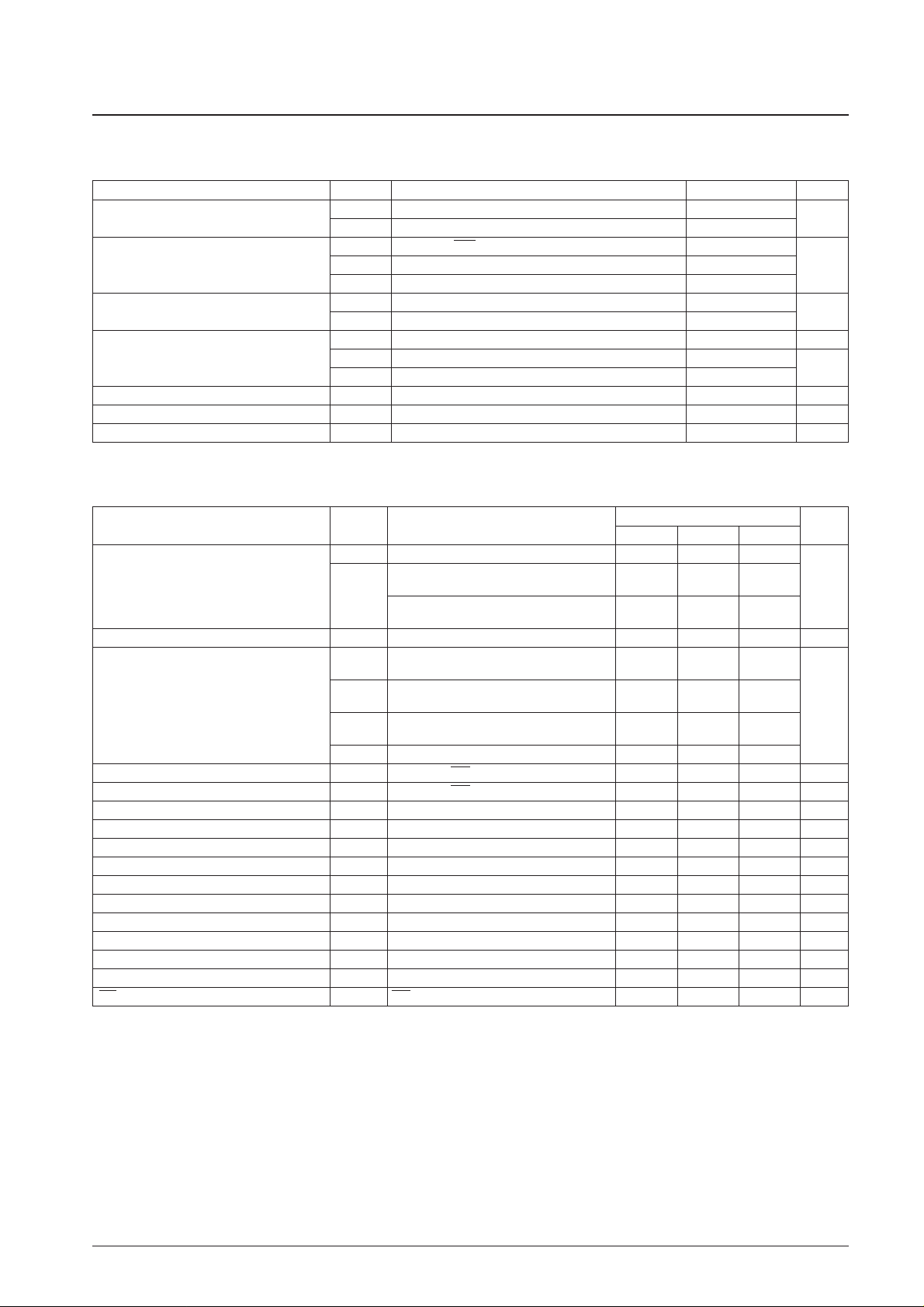
unit: mm
3181B-SQFP100
21.6
0.8
3.0max
1.6
17.2
0.825
130
31
50
51
80
81
1.6
0.575
0.575
0.15
2.7
15.6
0.3
20.0
23.2
14.0
0.65
0.825
100
0.8
0.65
0.1
Preliminary
SANYO: QFP100E
[LC75878E]
0.2
1.0
1.0
16.0
14.0
0.5
16.0
14.0
0.5
1.0
1.0
0.145
1.4
1.6max
0.5 0.5
100
125
26
50
5175
76
0.1
SANYO: SQFP100
[LC75878W]
LC75878E, 75878W
SANYO Electric Co.,Ltd. Semiconductor Company
TOKYO OFFICE Tokyo Bldg., 1-10, 1 Chome, Ueno, Taito-ku, TOKYO, 110-8534 JAPAN
1/8 to 1/10 Duty General-Purpose LCD Display Drivers
CMOS IC
Any and all SANYO products described or contained herein do not have specifications that can handle
applications that require extremely high levels of reliability, such as life-support systems, aircraft’s
control systems, or other applications whose failure can be reasonably expected to result in serious
physical and/or material damage. Consult with your SANYO representative nearest you before using
any SANYO products described or contained herein in such applications.
SANYO assumes no responsibility for equipment failures that result from using products at values that
exceed, even momentarily, rated values (such as maximum ratings, operating condition ranges, or other
parameters) listed in products specifications of any and all SANYO products described or contained
herein.
• CCB is a trademark of SANYO ELECTRIC CO., LTD.
• CCB is SANYO’s original bus format and all the bus
addresses are controlled by SANYO.
Page 2

No. 6473-2/33
LC75878E, 75878W
Pin Assignment
Page 3
No. 6473-3/33
LC75878E, 75878W
Parameter Symbol Conditions Ratings Unit
Maximum supply voltage
V
DD
max V
DD
–0.3 to +7.0
V
V
LCD
max V
LCD
–0.3 to +12.0
V
IN
1 CE, CL, DI, INH –0.3 to +7.0
Input voltage V
IN
2 OSC –0.3 to VDD+0.3 V
V
IN
3V
LCD
1, V
LCD
2, V
LCD
3, V
LCD
4 –0.3 to V
LCD
+0.3
Output voltage
V
OUT
1 OSC, P1 to P4 –0.3 to VDD+0.3
V
V
OUT
2V
LCD
0, S1 to S75, COM1 to COM10 –0.3 to V
LCD
+0.3
I
OUT
1 S1 to S75 300 µA
Output current I
OUT
2 COM1 to COM10 3
mA
I
OUT
3 P1 to P4 5
Allowable power dissipation Pd max Ta = 85°C 200 mW
Operating temperature Topr –40 to +85 °C
Storage temperature Tstg –55 to +125 °C
Specifications
Absolute Maximum Ratings at Ta=25°C, VSS=0V
Parameter Symbol Conditions
Ratings
Unit
min typ max
V
DDVDD
2.7 6.0
V
LCD
, When the display contrast adjustment 7.0 11.0
Supply voltage
V
LCD
circuit is used V
V
LCD
, When the display contrast adjustment 4.5 11.0
circuit is not used
Output voltage V
LCD
0V
LCD
0
V
LCD
4 + 4.5
V
LCD
V
V
LCD
1V
LCD
1
3/4
V
LCD
0
(V
LCD
0–V
LCD
4)
V
LCD
2V
LCD
2
2/4
V
LCD
0
Input voltage
(V
LCD
0–V
LCD
4)
V
V
LCD
3V
LCD
3
1/4
V
LCD
0
(V
LCD
0–V
LCD
4)
V
LCD
4V
LCD
4 0 1.5
Input high level voltage V
IH
CE, CL, DI, INH 0.8 V
DD
6.0 V
Input low level voltage V
IL
CE, CL, DI, INH 0 0.2 V
DD
V
Recommended external resistance R
OSC
OSC 43 kΩ
Recommended external capacitance C
OSC
OSC 680 pF
Guaranteed oscillation range f
OSC
OSC 25 50 100 kHz
Data setup time t
ds
CL, DI :Figure 2 160 ns
Data hold time t
dh
CL, DI :Figure 2 160 ns
CE wait time t
cp
CE, CL :Figure 2 160 ns
CE setup time t
cs
CE, CL :Figure 2 160 ns
CE hold time t
ch
CE, CL :Figure 2 160 ns
High level clock pulse width tø
H
CL :Figure 2 160 ns
Low level clock pulse width tø
L
CL :Figure 2 160 ns
INH switching time t
c
INH, CE :Figures 3, 4, and 5 10 µs
Allowable Operating Ranges at Ta = –40 to +85°C, VSS=0V
Page 4
No. 6473-4/33
LC75878E, 75878W
Parameter Symbol Conditions
Ratings
Unit
min typ max
Hysteresis V
H
CE, CL, DI, INH 0.1 V
DD
V
Input high level current I
IH
CE, CL, DI, INH: VI= 6.0 V 5.0 µA
Input low level current I
IL
CE, CL, DI, INH: VI= 0 V –5.0 µA
V
OH
1 S1 to S75: IO= –20 µA
V
LCD
0 – 0.6
Output high level voltage VOH2 COM1 to COM10: IO= –100 µA
V
LCD
0 – 0.6
V
V
OH
3 P1 to P4: IO= –1 mA VDD– 1.0
V
OL
1 S1 to S75: IO= 20 µA
V
LCD
4 + 0.6
Output low level voltage VOL2 COM1 to COM10: IO= 100 µA
V
LCD
4 + 0.6
V
V
OL
3 P1 to P4: IO= 1 mA 1.0
2/4 2/4
V
MID
1 S1 to S75: IO= ±20 µA
(V
LCD
0 – V
LCD
4) (V
LCD
0 – V
LCD
4)
–0.6 +0.6
3/4 3/4
Output middle level voltage * V
MID
2 COM1 to COM10: IO= ±100 µA
(V
LCD
0 – V
LCD
4) (V
LCD
0 – V
LCD
4)
V
–0.6 +0.6
1/4 1/4
V
MID
3 COM1 to COM10: IO= ±100 µA
(V
LCD
0 – V
LCD
4) (V
LCD
0 – V
LCD
4)
–0.6 +0.6
Oscillator frequency fosc OSC: R
OSC
= 43 kΩ, C
OSC
= 680 pF 40 50 60 kHz
I
DD
1VDD: Power saving mode 5
I
DD
2VDD: VDD= 6.0 V,
outputs open, fosc = 50 kHz
200 400
I
LCD
1V
LCD
: Power saving mode 5
V
LCD
: V
LCD
= 11.0 V
I
LCD
2
Outputs open
500 1000 µA
Current drain
fosc = 50 kHz
When the display contrast adjustment circuit is used.
V
LCD
: V
LCD
= 11.0 V
I
LCD
3
Outputs open
250 500
fosc = 50 kHz
When the display contrast adjustment circuit is not used.
Electrical Characteristics for the Allowable Operating Ranges
Note: * Excluding the bias voltage generation divider resistor built into V
LCD
0, V
LCD
1, V
LCD
2 , V
LCD
3, and V
LCD
4. (See Figure 1.)
Page 5

No. 6473-5/33
LC75878E, 75878W
Figure 1
• When CL is stopped at the low level
Figure 2
• When CL is stopped at the high level
To the common and segment drivers
Excluding these resistors
CONTRAST
ADJUSTER
Page 6
No. 6473-6/33
LC75878E, 75878W
Block Diagram
GENERAL PORT
COMMON
DRIVER
SEGMENT DRIVER & LATCH
CONTROL
REGISTER
CLOCK
GENERATOR
CONTRAST
ADJUSTER
SHIFT REGISTER
CCB INTERFACE
Page 7

No. 6473 -7/39
LC75878E, 75878W
Pin
Pin No.
Function Active I/O
Handling
LC75878E LC75878W
when unused
S1 to S73 3 to 75 1 to 73 Segment driver outputs.
S74/COM10 76 74 The S74/COM10 and S75/COM9 pins can be used as common — ●● Open
S75/COM9 77 75 driver outputs under the control data.
COM1 to COM8
85 to 78 83 to 76 Common driver outputs. — ●● Open
P1 to P4 86 to 89 84 to 87 General-purpose output ports. — ●● Open
OSC 98 96 — I/O V
DD
CE 100 98 HI
CL 1 99 I GND
DI 2 100 —I
INH 99 97 L I GND
V
LCD
092 90 — O Open
V
LCD
193 91 — I Open
V
LCD
294 92 — I Open
V
LCD
395 93 — I Open
V
LCD
496 94 — I GND
V
DD
90 88 —— —
V
LCD
91 89 —— —
V
SS
97 95 Power supply connection. Connect to ground. — — —
Pin Functions
Oscillator connection.
An oscillator circuit is formed by connecting an external resistor and
capacitor at this pin.
Serial data transfer inputs.
These pins are connected to the microcontroller.
CE :Chip enable
CL :Synchronization clock
DI :Transfer data
▲
Input that turns the display off and forces the general-purpose output
ports low.
• When INH is low (V
SS
)
• Display off
S1 to S73 = “L” (V
LCD
4).
S74/COM10, S75/COM9 = “L” (V
LCD
4)
COM1 to COM8 = “L” (V
LCD
4).
• General-purpose output ports P1 to P4 = low (V
SS
)
• When INH is high (V
DD
)
• Display on
• The states of the general-purpose output ports can be set by
the PC1 to PC4 control data.
However, serial data can be transferred when the INH pin is low.
LCD drive 3/4 bias voltage (middle level) supply pin. This pin can be
used to supply the 3/4 (V
LCD
0 – V
LCD
4) voltage level externally.
LCD drive 2/4 bias voltage (middle level) supply pin. This pin can be
used to supply the 2/4 (V
LCD
0 – V
LCD
4) voltage level externally.
LCD drive 1/4 bias voltage (middle level) supply pin. This pin can be
used to supply the 1/4 (V
LCD
0 – V
LCD
4) voltage level externally.
LCD drive 0/4 bias voltage (low level) supply pin. Fine adjustment of the
display contrast can be implemented by connecting an external variable
resistor to this pin.
However, (V
LCD
0 – V
LCD
4) must be greater than or equal to 4.5 V, and
V
LCD
4 must be in the range 0 V to 1.5 V, inclusive.
Logic block power supply connection. Provide a voltage of between 2.7
and 6.0V.
LCD driver block power supply connection. Provide a voltage of between
7.0 and 11.0 V when the display contrast adjustment circuit is used and
provide a voltage of between 4.5 and 11.0 V when the circuit is not used.
LCD drive 4/4 bias voltage (high level) supply pin. The level on this pin
can be changed by the display contrast adjustment circuit.
However, (V
LCD
0 – V
LCD
4) must be greater than or equal to 4.5 V.
Also,external power must not be applied to this pin since the pin circuit
includes the display contrast adjustment circuit.
Page 8
No. 6473-8/33
LC75878E, 75878W
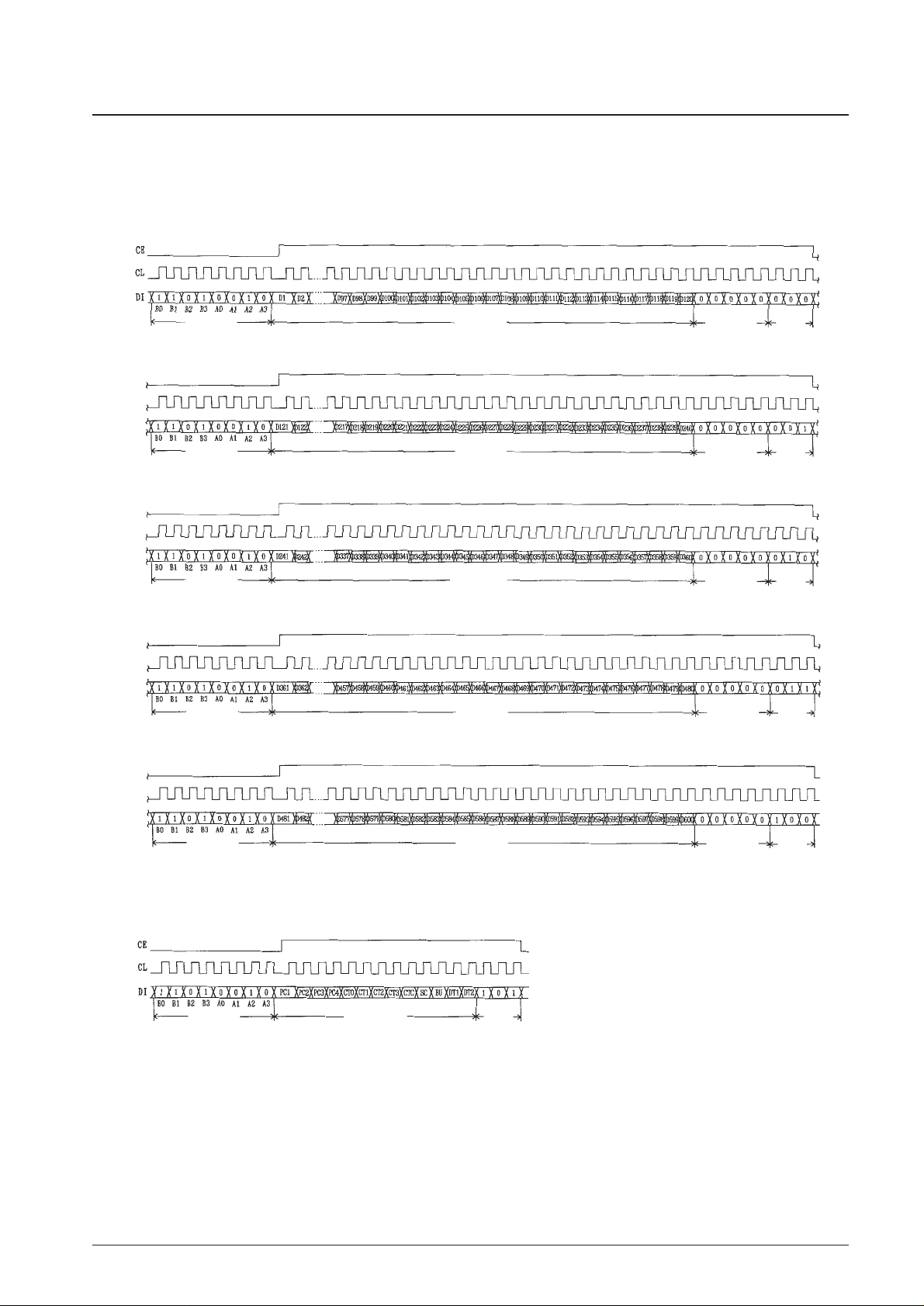
Serial Data Transfer Format
1. 1/8 duty
① When CL is stopped at the low level
• When the display data is transferred.
• When the control data is transferred.
Note: B0 to B3, A0 to A3
......
CCB address
DD
................................
Direction data
Display
data
120 bits
Fixed
data
5 bits
DD
3 bits
CCB
address
8 bits
CCB
address
8 bits
CCB
address
8 bits
Display
data
120 bits
Fixed
data
5 bits
Fixed
data
5 bits
Display
data
120 bits
DD
3 bits
DD
3 bits
CCB
address
8 bits
CCB
address
8 bits
Display
data
120 bits
Display
data
120 bits
Fixed
data
5 bits
Fixed
data
5 bits
DD
3 bits
DD
3 bits
CCB
address
8 bits
Control
data
13 bits
DD
3 bits
Page 9
No. 6473-9/33
LC75878E, 75878W
② When CL is stopped at the high level
• When the display data is transferred.
Note: B0 to B3, A0 to A3
......
CCB address
DD
................................
Direction data
• CCB address: ....4BH
• D1 to D600: ........ Display data
• PC1 to PC4: ........ General-purpose output port state setting data
• CT0 to CT3, CTC: Display contrast setting data
• SC: ...................... Segment on/off control data
• BU: ...................... Normal mode/power saving mode control data
• DT1, DT2:............ Display technique setting data
• When the control data is transferred.
CCB
address
8 bits
Display
data
120 bits
Fixed
data
5 bits
DD
3 bits
Control
data
13 bits
CCB
address
8 bits
CCB
address
8 bits
CCB
address
8 bits
CCB
address
8 bits
Display
data
120 bits
Display
data
120 bits
Display
data
120 bits
Display
data
120 bits
Fixed
data
5 bits
Fixed
data
5 bits
Fixed
data
5 bits
Fixed
data
5 bits
DD
3 bits
DD
3 bits
DD
3 bits
DD
3 bits
CCB
address
8 bits
DD
3 bits
Page 10
No. 6473-10/33
LC75878E, 75878W
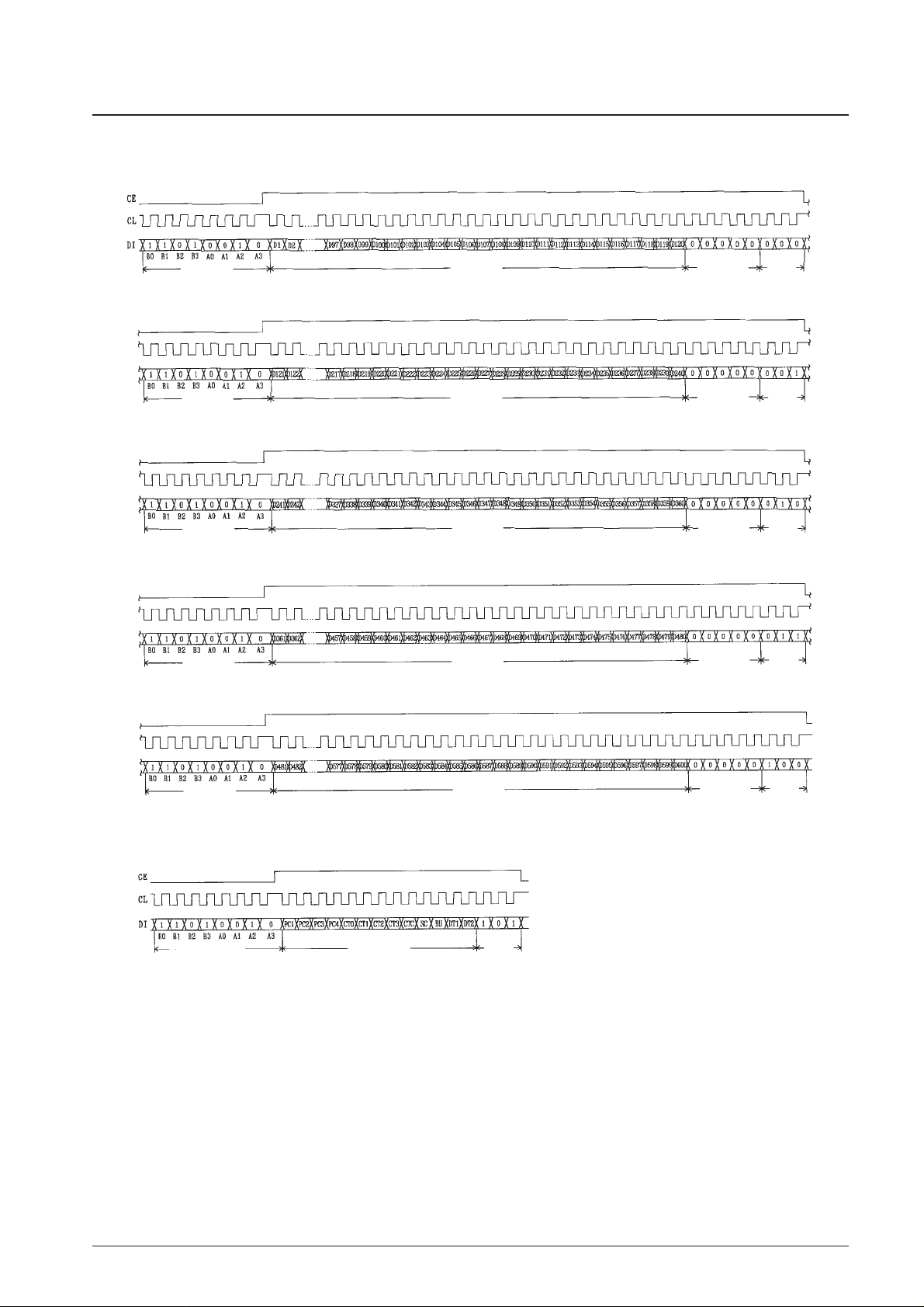
2. 1/9 duty
① When CL is stopped at the low level
• When the display data is transferred.
• When the control data is transferred.
Note: B0 to B3, A0 to A3
......
CCB address
DD
................................
Direction data
Control
data
13 bits
CCB
address
8 bits
Display
data
135 bits
Fixed
data
6 bits
DD
3 bits
CCB
address
8 bits
CCB
address
8 bits
CCB
address
8 bits
CCB
address
8 bits
Display
data
135 bits
Display
data
135 bits
Display
data
135 bits
Display
data
126 bits
Fixed
data
6 bits
Fixed
data
6 bits
Fixed
data
6 bits
Fixed
data
15 bits
DD
3 bits
DD
3 bits
DD
3 bits
DD
3 bits
DD
3 bits
CCB
address
8 bits
Page 11

No. 6473-11/33
LC75878E, 75878W
② When CL is stopped at the high level
• When the display data is transferred.
Note: B0 to B3, A0 to A3
......
CCB address
DD
................................
Direction data
• CCB address:...... 4BH
• D1 to D666: ........ Display data
• PC1 to PC4: ........ General-purpose output port state setting data
• CT0 to CT3, CTC: Display contrast setting data
• SC: ...................... Segment on/off control data
• BU: ...................... Normal mode/power saving mode control data
• DT1, DT2:............ Display technique setting data
• When the control data is transferred.
Control
data
13 bits
CCB
address
8 bits
Display
data
135 bits
Fixed
data
6 bits
DD
3 bits
CCB
address
8 bits
Display
data
135 bits
Fixed
data
6 bits
DD
3 bits
CCB
address
8 bits
Display
data
135 bits
Fixed
data
6 bits
DD
3 bits
CCB
address
8 bits
Display
data
135 bits
Fixed
data
6 bits
DD
3 bits
CCB
address
8 bits
Display
data
126 bits
Fixed
data
15 bits
DD
3 bits
CCB
address
8 bits
DD
3 bits
Page 12

No. 6473-12/33
LC75878E, 75878W
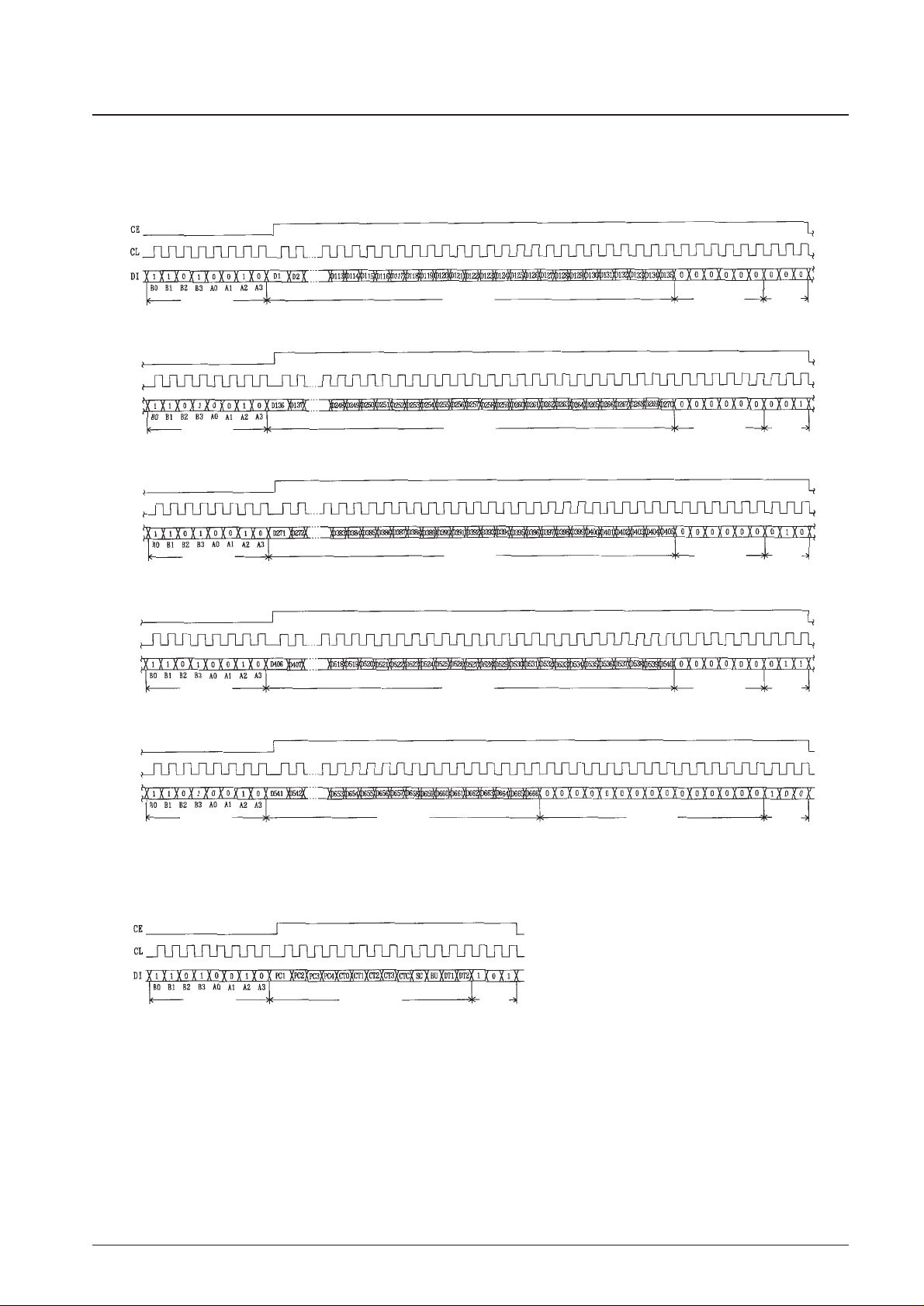
3. 1/10 duty
① When CL is stopped at the low level
• When the display data is transferred.
• When the control data is transferred.
Note: B0 to B3, A0 to A3
......
CCB address
DD
................................
Direction data
Control
data
13 bits
CCB
address
8 bits
Display
data
150 bits
Fixed
data
7 bits
DD
3 bits
CCB
address
8 bits
Display
data
150 bits
Fixed
data
7 bits
DD
3 bits
CCB
address
8 bits
Display
data
150 bits
Fixed
data
7 bits
DD
3 bits
CCB
address
8 bits
Display
data
150 bits
Fixed
data
7 bits
DD
3 bits
CCB
address
8 bits
Display
data
130 bits
Fixed
data
27 bits
DD
3 bits
CCB
address
8 bits
DD
3 bits
Page 13

No. 6473-13/33
LC75878E, 75878W
② When CL is stopped at the high level
• When the display data is transferred.
Note: B0 to B3, A0 to A3
......
CCB address
DD
................................
Direction data
• CCB address:...... 4BH
• D1 to D730: ........ Display data
• PC1 to PC4: ........ General-purpose output port state setting data
• CT0 to CT3, CTC: Display contrast setting data
• SC: ...................... Segment on/off control data
• BU: ...................... Normal mode/power saving mode control data
• DT1, DT2:............ Display technique setting data
• When the control data is transferred.
Control
data
13 bits
CCB
address
8 bits
Display
data
150 bits
Fixed
data
7 bits
DD
3 bits
CCB
address
8 bits
Display
data
150 bits
Fixed
data
7 bits
DD
3 bits
CCB
address
8 bits
Display
data
150 bits
Fixed
data
7 bits
DD
3 bits
CCB
address
8 bits
Display
data
150 bits
Fixed
data
7 bits
DD
3 bits
CCB
address
8 bits
Display
data
130 bits
Fixed
data
27 bits
DD
3 bits
CCB
address
8 bits
DD
3 bits
Page 14

No. 6473-14/33
LC75878E, 75878W
Control Data Functions
For example, if PC1 and PC2 are set to 1, and PC3 and PC4 are set to 0, then the output pins P1 and P2 will output high
levels (VDD) and the output pins P3 and P4 will output low levels (VSS).
1. PC1 to PC4: General-purpose output port state setting data
These control data bits set the states of the general-purpose output ports P1 to P4.
Output pin P1 P2 P3 P4
General-purpose output port state setting data PC1 PC2 PC3 PC4
2. CT0 to CT3, CTC: Display contrast setting data
These control data bits set the display contrast.
CT0 to CT3: Display contrast setting (11 steps)
CT0 CT1 CT2 CT3 LCD drive 4/4 bias voltage supply V
LCD
0 level
0 0 0 0 0.94 V
LCD
= V
LCD
– (0.03 V
LCD
× 2)
1 0 0 0 0.91 V
LCD
= V
LCD
– (0.03 V
LCD
× 3)
0 1 0 0 0.88 V
LCD
= V
LCD
– (0.03 V
LCD
× 4)
1 1 0 0 0.85 V
LCD
= V
LCD
– (0.03 V
LCD
× 5)
0 0 1 0 0.82 V
LCD
= V
LCD
– (0.03 V
LCD
× 6)
1 0 1 0 0.79 V
LCD
= V
LCD
– (0.03 V
LCD
× 7)
0 1 1 0 0.76 V
LCD
= V
LCD
– (0.03 V
LCD
× 8)
1 1 1 0 0.73 V
LCD
= V
LCD
– (0.03 V
LCD
× 9)
0 0 0 1 0.70 V
LCD
= V
LCD
– (0.03 V
LCD
× 10)
1 0 0 1 0.67 V
LCD
= V
LCD
– (0.03 V
LCD
× 11)
0 1 0 1 0.64 V
LCD
= V
LCD
– (0.03 V
LCD
× 12)
CTC: Display contrast adjustment circuit state setting
Note that although the display contrast can be adjusted by operating the built-in display contrast adjustment circuit, it is
also possible to apply fine adjustments to the contrast by connecting an external variable resistor to the V
LCD
4 pin and
modifying the V
LCD
4 pin voltage. However, the following conditions must be met: (V
LCD
0 – V
LCD
4) ≥ 4.5 V, and 1.5 V
≥ V
LCD
4 ≥ 0 V.
CTC Display contrast adjustment circuit state
0 The display contrast adjustment circuit is disabled, and the V
LCD
0 pin level is forced to the V
LCD
level.
1 The display contrast adjustment circuit operates and the display contrast is adjusted.
Page 15

No. 6473-15/33
LC75878E, 75878W
However, note that when the segments are turned off by setting SC to 1, the segments are turned off by outputting segment off waveforms from the segment
output pins.
Notes: Sn (n = 74 or 75): Segment outputs
COMn (n = 9 or 10): Common outputs
SC Display state
0On
1 Off
3. SC: Segment on/off control data
This control data bit controls the on/off state of the segments.
BU Mode
0 Normal mode
Power saving mode
1
The common and segment pins go to the V
LCD
4 level and the oscillator on the OSC pin is stopped. Note that the states of the
general-purpose output ports P1 to P4 are set by PC1 to PC4 in the control data during power saving mode as well as normal mode.
4. BU: Normal mode/power saving mode control data
This control data bit controls the normal mode and power saving mode.
5. DT1, DT2: Display technique setting data
This control data bits set the display technique.
DT1 DT2 Display technique
Output pins
S75/COM9 S74/COM10
0 0 1/8 duty 1/4 bias drive S75 S74
1 0 1/9 duty 1/4 bias drive COM9 S74
0 1 1/10 duty 1/4 bias drive COM9 COM10
Page 16

No. 6473-16/33
LC75878E, 75878W
Display Data and Output Pin Correspondence
• 1/8 duty
Output Pin COM1 COM2 COM3 COM4 COM5 COM6 COM7 COM8
S1 D1 D2 D3 D4 D5 D6 D7 D8
S2 D9 D10 D11 D12 D13 D14 D15 D16
S3 D17 D18 D19 D20 D21 D22 D23 D24
S4 D25 D26 D27 D28 D29 D30 D31 D32
S5 D33 D34 D35 D36 D37 D38 D39 D40
S6 D41 D42 D43 D44 D45 D46 D47 D48
S7 D49 D50 D51 D52 D53 D54 D55 D56
S8 D57 D58 D59 D60 D61 D62 D63 D64
S9 D65 D66 D67 D68 D69 D70 D71 D72
S10 D73 D74 D75 D76 D77 D78 D79 D80
S11 D81 D82 D83 D84 D85 D86 D87 D88
S12 D89 D90 D91 D92 D93 D94 D95 D96
S13 D97 D98 D99 D100 D101 D102 D103 D104
S14 D105 D106 D107 D108 D109 D110 D111 D112
S15 D113 D114 D115 D116 D117 D118 D119 D120
S16 D121 D122 D123 D124 D125 D126 D127 D128
S17 D129 D130 D131 D132 D133 D134 D135 D136
S18 D137 D138 D139 D140 D141 D142 D143 D144
S19 D145 D146 D147 D148 D149 D150 D151 D152
S20 D153 D154 D155 D156 D157 D158 D159 D160
S21 D161 D162 D163 D164 D165 D166 D167 D168
S22 D169 D170 D171 D172 D173 D174 D175 D176
S23 D177 D178 D179 D180 D181 D182 D183 D184
S24 D185 D186 D187 D188 D189 D190 D191 D192
S25 D193 D194 D195 D196 D197 D198 D199 D200
S26 D201 D202 D203 D204 D205 D206 D207 D208
S27 D209 D210 D211 D212 D213 D214 D215 D216
S28 D217 D218 D219 D220 D221 D222 D223 D224
S29 D225 D226 D227 D228 D229 D230 D231 D232
S30 D233 D234 D235 D236 D237 D238 D239 D240
S31 D241 D242 D243 D244 D245 D246 D247 D248
S32 D249 D250 D251 D252 D253 D254 D255 D256
S33 D257 D258 D259 D260 D261 D262 D263 D264
S34 D265 D266 D267 D268 D269 D270 D271 D272
S35 D273 D274 D275 D276 D277 D278 D279 D280
S36 D281 D282 D283 D284 D285 D286 D287 D288
S37 D289 D290 D291 D292 D293 D294 D295 D296
S38 D297 D298 D299 D300 D301 D302 D303 D304
S39 D305 D306 D307 D308 D309 D310 D311 D312
S40 D313 D314 D315 D316 D317 D318 D319 D320
S41 D321 D322 D323 D324 D325 D326 D327 D328
S42 D329 D330 D331 D332 D333 D334 D335 D336
S43 D337 D338 D339 D340 D341 D342 D343 D344
S44 D345 D346 D347 D348 D349 D350 D351 D352
S45 D353 D354 D355 D356 D357 D358 D359 D360
Continued on next page.
Page 17

No. 6473-17/33
LC75878E, 75878W
Output Pin COM1 COM2 COM3 COM4 COM5 COM6 COM7 COM8
S46 D361 D362 D363 D364 D365 D366 D367 D368
S47 D369 D370 D371 D372 D373 D374 D375 D376
S48 D377 D378 D379 D380 D381 D382 D383 D384
S49 D385 D386 D387 D388 D389 D390 D391 D392
S50 D393 D394 D395 D396 D397 D398 D399 D400
S51 D401 D402 D403 D404 D405 D406 D407 D408
S52 D409 D410 D411 D412 D413 D414 D415 D416
S53 D417 D418 D419 D420 D421 D422 D423 D424
S54 D425 D426 D427 D428 D429 D430 D431 D432
S55 D433 D434 D435 D436 D437 D438 D439 D440
S56 D441 D442 D443 D444 D445 D446 D447 D448
S57 D449 D450 D451 D452 D453 D454 D455 D456
S58 D457 D458 D459 D460 D461 D462 D463 D464
S59 D465 D466 D467 D468 D469 D470 D471 D472
S60 D473 D474 D475 D476 D477 D478 D479 D480
S61 D481 D482 D483 D484 D485 D486 D487 D488
S62 D489 D490 D491 D492 D493 D494 D495 D496
S63 D497 D498 D499 D500 D501 D502 D503 D504
S64 D505 D506 D507 D508 D509 D510 D511 D512
S65 D513 D514 D515 D516 D517 D518 D519 D520
S66 D521 D522 D523 D524 D525 D526 D527 D528
S67 D529 D530 D531 D532 D533 D534 D535 D536
S68 D537 D538 D539 D540 D541 D542 D543 D544
S69 D545 D546 D547 D548 D549 D550 D551 D552
S70 D553 D554 D555 D556 D557 D558 D559 D560
S71 D561 D562 D563 D564 D565 D566 D567 D568
S72 D569 D570 D571 D572 D573 D574 D575 D576
S73 D577 D578 D579 D580 D581 D582 D583 D584
S74/COM10 D585 D586 D587 D588 D589 D590 D591 D592
S75/COM9 D593 D594 D595 D596 D597 D598 D599 D600
Continued from preceding page.
For example, the table below lists the segment output states for the S11 output pin.
Note: Applies when the S74/COM10 and S75/COM9 output pins are set to their segment output function.
Display data
Output pin state (S11)
D81 D82 D83 D84 D85 D86 D87 D88
0 0 0 0 0 0 0 0 The LCD segments for COM1 to COM8 are off
1 0 0 0 0 0 0 0 The LCD segment for COM1 is on
0 1 0 0 0 0 0 0 The LCD segment for COM2 is on
0 0 1 0 0 0 0 0 The LCD segment for COM3 is on
0 0 0 1 0 0 0 0 The LCD segment for COM4 is on
0 0 0 0 1 0 0 0 The LCD segment for COM5 is on
0 0 0 0 0 1 0 0 The LCD segment for COM6 is on
0 0 0 0 0 0 1 0 The LCD segment for COM7 is on
0 0 0 0 0 0 0 1 The LCD segment for COM8 is on
1 1 1 1 1 1 1 1 The LCD segments for COM1 to COM8 are on
Page 18

No. 6473-18/33
LC75878E, 75878W
• 1/9 duty
Output Pin COM1 COM2 COM3 COM4 COM5 COM6 COM7 COM8 COM9
S1 D1 D2 D3 D4 D5 D6 D7 D8 D9
S2 D10 D11 D12 D13 D14 D15 D16 D17 D18
S3 D19 D20 D21 D22 D23 D24 D25 D26 D27
S4 D28 D29 D30 D31 D32 D33 D34 D35 D36
S5 D37 D38 D39 D40 D41 D42 D43 D44 D45
S6 D46 D47 D48 D49 D50 D51 D52 D53 D54
S7 D55 D56 D57 D58 D59 D60 D61 D62 D63
S8 D64 D65 D66 D67 D68 D69 D70 D71 D72
S9 D73 D74 D75 D76 D77 D78 D79 D80 D81
S10 D82 D83 D84 D85 D86 D87 D88 D89 D90
S11 D91 D92 D93 D94 D95 D96 D97 D98 D99
S12 D100 D101 D102 D103 D104 D105 D106 D107 D108
S13 D109 D110 D111 D112 D113 D114 D115 D116 D117
S14 D118 D119 D120 D121 D122 D123 D124 D125 D126
S15 D127 D128 D129 D130 D131 D132 D133 D134 D135
S16 D136 D137 D138 D139 D140 D141 D142 D143 D144
S17 D145 D146 D147 D148 D149 D150 D151 D152 D153
S18 D154 D155 D156 D157 D158 D159 D160 D161 D162
S19 D163 D164 D165 D166 D167 D168 D169 D170 D171
S20 D172 D173 D174 D175 D176 D177 D178 D179 D180
S21 D181 D182 D183 D184 D185 D186 D187 D188 D189
S22 D190 D191 D192 D193 D194 D195 D196 D197 D198
S23 D199 D200 D201 D202 D203 D204 D205 D206 D207
S24 D208 D209 D210 D211 D212 D213 D214 D215 D216
S25 D217 D218 D219 D220 D221 D222 D223 D224 D225
S26 D226 D227 D228 D229 D230 D231 D232 D233 D234
S27 D235 D236 D237 D238 D239 D240 D241 D242 D243
S28 D244 D245 D246 D247 D248 D249 D250 D251 D252
S29 D253 D254 D255 D256 D257 D258 D259 D260 D261
S30 D262 D263 D264 D265 D266 D267 D268 D269 D270
S31 D271 D272 D273 D274 D275 D276 D277 D278 D279
S32 D280 D281 D282 D283 D284 D285 D286 D287 D288
S33 D289 D290 D291 D292 D293 D294 D295 D296 D297
S34 D298 D299 D300 D301 D302 D303 D304 D305 D306
S35 D307 D308 D309 D310 D311 D312 D313 D314 D315
S36 D316 D317 D318 D319 D320 D321 D322 D323 D324
S37 D325 D326 D327 D328 D329 D330 D331 D332 D333
S38 D334 D335 D336 D337 D338 D339 D340 D341 D342
S39 D343 D344 D345 D346 D347 D348 D349 D350 D351
S40 D352 D353 D354 D355 D356 D357 D358 D359 D360
S41 D361 D362 D363 D364 D365 D366 D367 D368 D369
S42 D370 D371 D372 D373 D374 D375 D376 D377 D378
S43 D379 D380 D381 D382 D383 D384 D385 D386 D387
S44 D388 D389 D390 D391 D392 D393 D394 D395 D396
S45 D397 D398 D399 D400 D401 D402 D403 D404 D405
Continued on next page.
Page 19

No. 6473-19/33
LC75878E, 75878W
Continued from preceding page.
Output Pin COM1 COM2 COM3 COM4 COM5 COM6 COM7 COM8 COM9
S46 D406 D407 D408 D409 D410 D411 D412 D413 D414
S47 D415 D416 D417 D418 D419 D420 D421 D422 D423
S48 D424 D425 D426 D427 D428 D429 D430 D431 D432
S49 D433 D434 D435 D436 D437 D438 D439 D440 D441
S50 D442 D443 D444 D445 D446 D447 D448 D449 D450
S51 D451 D452 D453 D454 D455 D456 D457 D458 D459
S52 D460 D461 D462 D463 D464 D465 D466 D467 D468
S53 D469 D470 D471 D472 D473 D474 D475 D476 D477
S54 D478 D479 D480 D481 D482 D483 D484 D485 D486
S55 D487 D488 D489 D490 D491 D492 D493 D494 D495
S56 D496 D497 D498 D499 D500 D501 D502 D503 D504
S57 D505 D506 D507 D508 D509 D510 D511 D512 D513
S58 D514 D515 D516 D517 D518 D519 D520 D521 D522
S59 D523 D524 D525 D526 D527 D528 D529 D530 D531
S60 D532 D533 D534 D535 D536 D537 D538 D539 D540
S61 D541 D542 D543 D544 D545 D546 D547 D548 D549
S62 D550 D551 D552 D553 D554 D555 D556 D557 D558
S63 D559 D560 D561 D562 D563 D564 D565 D566 D567
S64 D568 D569 D570 D571 D572 D573 D574 D575 D576
S65 D577 D578 D579 D580 D581 D582 D583 D584 D585
S66 D586 D587 D588 D589 D590 D591 D592 D593 D594
S67 D595 D596 D597 D598 D599 D600 D601 D602 D603
S68 D604 D605 D606 D607 D608 D609 D610 D611 D612
S69 D613 D614 D615 D616 D617 D618 D619 D620 D621
S70 D622 D623 D624 D625 D626 D627 D628 D629 D630
S71 D631 D632 D633 D634 D635 D636 D637 D638 D639
S72 D640 D641 D642 D643 D644 D645 D646 D647 D648
S73 D649 D650 D651 D652 D653 D654 D655 D656 D657
S74/COM10 D658 D659 D660 D661 D662 D663 D664 D665 D666
For example, the table below lists the segment output states for the S11 output pin.
Note: Applies when the S74/COM10 output pin is set to its segment output function.
Display data
Output pin state (S11)
D91 D92 D93 D94 D95 D96 D97 D98 D99
0 0 0 0 0 0 0 0 0 The LCD segments for COM1 to COM9 are off
1 0 0 0 0 0 0 0 0 The LCD segment for COM1 is on
0 1 0 0 0 0 0 0 0 The LCD segment for COM2 is on
0 0 1 0 0 0 0 0 0 The LCD segment for COM3 is on
0 0 0 1 0 0 0 0 0 The LCD segment for COM4 is on
0 0 0 0 1 0 0 0 0 The LCD segment for COM5 is on
0 0 0 0 0 1 0 0 0 The LCD segment for COM6 is on
0 0 0 0 0 0 1 0 0 The LCD segment for COM7 is on
0 0 0 0 0 0 0 1 0 The LCD segment for COM8 is on
0 0 0 0 0 0 0 0 1 The LCD segment for COM9 is on
1 1 1 1 1 1 1 1 1 The LCD segments for COM1 to COM9 are on
Page 20

No. 6473-20/33
LC75878E, 75878W
• 1/10 duty
Output Pin COM1 COM2 COM3 COM4 COM5 COM6 COM7 COM8 COM9 COM10
S1 D1 D2 D3 D4 D5 D6 D7 D8 D9 D10
S2 D11 D12 D13 D14 D15 D16 D17 D18 D19 D20
S3 D21 D22 D23 D24 D25 D26 D27 D28 D29 D30
S4 D31 D32 D33 D34 D35 D36 D37 D38 D39 D40
S5 D41 D42 D43 D44 D45 D46 D47 D48 D49 D50
S6 D51 D52 D53 D54 D55 D56 D57 D58 D59 D60
S7 D61 D62 D63 D64 D65 D66 D67 D68 D69 D70
S8 D71 D72 D73 D74 D75 D76 D77 D78 D79 D80
S9 D81 D82 D83 D84 D85 D86 D87 D88 D89 D90
S10 D91 D92 D93 D94 D95 D96 D97 D98 D99 D100
S11 D101 D102 D103 D104 D105 D106 D107 D108 D109 D110
S12 D111 D112 D113 D114 D115 D116 D117 D118 D119 D120
S13 D121 D122 D123 D124 D125 D126 D127 D128 D129 D130
S14 D131 D132 D133 D134 D135 D136 D137 D138 D139 D140
S15 D141 D142 D143 D144 D145 D146 D147 D148 D149 D150
S16 D151 D152 D153 D154 D155 D156 D157 D158 D159 D160
S17 D161 D162 D163 D164 D165 D166 D167 D168 D169 D170
S18 D171 D172 D173 D174 D175 D176 D177 D178 D179 D180
S19 D181 D182 D183 D184 D185 D186 D187 D188 D189 D190
S20 D191 D192 D193 D194 D195 D196 D197 D198 D199 D200
S21 D201 D202 D203 D204 D205 D206 D207 D208 D209 D210
S22 D211 D212 D213 D214 D215 D216 D217 D218 D219 D220
S23 D221 D222 D223 D224 D225 D226 D227 D228 D229 D230
S24 D231 D232 D233 D234 D235 D236 D237 D238 D239 D240
S25 D241 D242 D243 D244 D245 D246 D247 D248 D249 D250
S26 D251 D252 D253 D254 D255 D256 D257 D258 D259 D260
S27 D261 D262 D263 D264 D265 D266 D267 D268 D269 D270
S28 D271 D272 D273 D274 D275 D276 D277 D278 D279 D280
S29 D281 D282 D283 D284 D285 D286 D287 D288 D289 D290
S30 D291 D292 D293 D294 D295 D296 D297 D298 D299 D300
S31 D301 D302 D303 D304 D305 D306 D307 D308 D309 D310
S32 D311 D312 D313 D314 D315 D316 D317 D318 D319 D320
S33 D321 D322 D323 D324 D325 D326 D327 D328 D329 D330
S34 D331 D332 D333 D334 D335 D336 D337 D338 D339 D340
S35 D341 D342 D343 D344 D345 D346 D347 D348 D349 D350
S36 D351 D352 D353 D354 D355 D356 D357 D358 D359 D360
S37 D361 D362 D363 D364 D365 D366 D367 D368 D369 D370
S38 D371 D372 D373 D374 D375 D376 D377 D378 D379 D380
S39 D381 D382 D383 D384 D385 D386 D387 D388 D389 D390
S40 D391 D392 D393 D394 D395 D396 D397 D398 D399 D400
S41 D401 D402 D403 D404 D405 D406 D407 D408 D409 D410
S42 D411 D412 D413 D414 D415 D416 D417 D418 D419 D420
S43 D421 D422 D423 D424 D425 D426 D427 D428 D429 D430
S44 D431 D432 D433 D434 D435 D436 D437 D438 D439 D440
S45 D441 D442 D443 D444 D445 D446 D447 D448 D449 D450
Continued on next page.
Page 21

No. 6473-21/33
LC75878E, 75878W
Continued from preceding page.
Output Pin COM1 COM2 COM3 COM4 COM5 COM6 COM7 COM8 COM9 COM10
S46 D451 D452 D453 D454 D455 D456 D457 D458 D459 D460
S47 D461 D462 D463 D464 D465 D466 D467 D468 D469 D470
S48 D471 D472 D473 D474 D475 D476 D477 D478 D479 D480
S49 D481 D482 D483 D484 D485 D486 D487 D488 D489 D490
S50 D491 D492 D493 D494 D495 D496 D497 D498 D499 D500
S51 D501 D502 D503 D504 D505 D506 D507 D508 D509 D510
S52 D511 D512 D513 D514 D515 D516 D517 D518 D519 D520
S53 D521 D522 D523 D524 D525 D526 D527 D528 D529 D530
S54 D531 D532 D533 D534 D535 D536 D537 D538 D539 D540
S55 D541 D542 D543 D544 D545 D546 D547 D548 D549 D550
S56 D551 D552 D553 D554 D555 D556 D557 D558 D559 D560
S57 D561 D562 D563 D564 D565 D566 D567 D568 D569 D570
S58 D571 D572 D573 D574 D575 D576 D577 D578 D579 D580
S59 D581 D582 D583 D584 D585 D586 D587 D588 D589 D590
S60 D591 D592 D593 D594 D595 D596 D597 D598 D599 D600
S61 D601 D602 D603 D604 D605 D606 D607 D608 D609 D610
S62 D611 D612 D613 D614 D615 D616 D617 D618 D619 D620
S63 D621 D622 D623 D624 D625 D626 D627 D628 D629 D630
S64 D631 D632 D633 D634 D635 D636 D637 D638 D639 D640
S65 D641 D642 D643 D644 D645 D646 D647 D648 D649 D650
S66 D651 D652 D653 D654 D655 D656 D657 D658 D659 D660
S67 D661 D662 D663 D664 D665 D666 D667 D668 D669 D670
S68 D671 D672 D673 D674 D675 D676 D677 D678 D679 D680
S69 D681 D682 D683 D684 D685 D686 D687 D688 D689 D690
S70 D691 D692 D693 D694 D695 D696 D697 D698 D699 D700
S71 D701 D702 D703 D704 D705 D706 D707 D708 D709 D710
S72 D711 D712 D713 D714 D715 D716 D717 D718 D719 D720
S73 D721 D722 D723 D724 D725 D726 D727 D728 D729 D730
For example, the table below lists the segment output states for the S11 output pin.
Display data
Output pin state (S11)
D101 D102 D103 D104 D105 D106 D107 D108 D109 D110
0 0 0 0 0 0 0 0 0 0 The LCD segments for COM1 to COM10 are off
1 0 0 0 0 0 0 0 0 0 The LCD segment for COM1 is on
0 1 0 0 0 0 0 0 0 0 The LCD segment for COM2 is on
0 0 1 0 0 0 0 0 0 0 The LCD segment for COM3 is on
0 0 0 1 0 0 0 0 0 0 The LCD segment for COM4 is on
0 0 0 0 1 0 0 0 0 0 The LCD segment for COM5 is on
0 0 0 0 0 1 0 0 0 0 The LCD segment for COM6 is on
0 0 0 0 0 0 1 0 0 0 The LCD segment for COM7 is on
0 0 0 0 0 0 0 1 0 0 The LCD segment for COM8 is on
0 0 0 0 0 0 0 0 1 0 The LCD segment for COM9 is on
0 0 0 0 0 0 0 0 0 1 The LCD segment for COM10 is on
1 1 1 1 1 1 1 1 1 1 The LCD segments for COM1 to COM10 are on
Page 22

No. 6473-22/33
LC75878E, 75878W
1/8 Duty, 1/4 Bias Drive Technique
LCD driver output when all LCD segments
corresponding to COM1 to COM8 are turned off
LCD driver output when only LCD segments
corresponding to COM1 are turned on
LCD driver output when only LCD segments
corresponding to COM2 are turned on
LCD driver output when all LCD segments
corresponding to COM1 to COM8 are turned on
COM1
COM2
COM8
.
.
.
.
.
.
.
.
.
.
.
.
.
.
.
.
.
Page 23

No. 6473-23/33
LC75878E, 75878W
1/9 Duty, 1/4 Bias Drive Technique
LCD driver output when all LCD segments
corresponding to COM1 to COM9 are turned off
LCD driver output when only LCD segments
corresponding to COM1 are turned on
LCD driver output when only LCD segments
corresponding to COM2 are turned on
LCD driver output when all LCD segments
corresponding to COM1 to COM9 are turned on
COM1
COM2
COM9
.
.
.
.
.
.
.
.
.
.
.
.
.
.
.
.
.
Page 24

No. 6473-24/33
LC75878E, 75878W
1/10 Duty, 1/4 Bias Drive Technique
LCD driver output when all LCD segments
corresponding to COM1 to COM10 are turned off
LCD driver output when only LCD segments
corresponding to COM1 are turned on
LCD driver output when only LCD segments
corresponding to COM2 are turned on
LCD driver output when all LCD segments
corresponding to COM1 to COM10 are turned on
COM1
COM2
COM10
.
.
.
.
.
.
.
.
.
.
.
.
.
.
.
.
.
Page 25

No. 6473-25/33
LC75878E, 75878W
The INH Pin and Display Control
Since the IC internal data (the display data and the control data) is undefined when power is first applied, applications
should set the INH pin low at the same time as power is applied to turn off the display (This sets the S1 to S73,
S74/COM10, S75/COM9, and COM1 to COM8 to the V
LCD
4 level and the P1 to P4 to the VSSlevel.) and during this
period send serial data from the controller. The controller should then set the INH pin high after the data transfer has
completed. This procedure prevents meaningless displays at power on. (See figures 3, 4, and 5.)
Power Supply Sequence
The following sequences must be observed when power is turned on and off. (See figures 3, 4, and 5.)
• Power on :Logic block power supply(V
DD
) on → LCD driver block power supply(V
LCD
) on
• Power off:LCD driver block power supply(V
LCD
) off → Logic block power supply(VDD) off
However, if the logic and LCD driver blocks use a shared power supply, then the power supplies can be turned on and off
at the same time.
• t1 ≥ 0
• t2 > 0
• t3 ≥ 0 (t2 > t3)
• tc • • • 10 µs min
Internal data (D1 to D120)
Internal data (D121 to D240)
Internal data (D241 to D360)
Internal data (D361 to D480)
Undefined
Defined
Figure 3
INH
CE
V
LCD
V
DD
Undefined
Undefined
Undefined
Undefined
Undefined
Undefined
Undefined
Undefined
Undefined
Display and control data transfer
Defined
Defined
Defined
Defined
Internal data (D481 to D600)
Undefined
Defined
Undefined
• 1/8 duty
Internal data (PC1 to PC4, CT0 to
CT3, CTC, SC, BU,
DT1, DT2)
Page 26

• 1/9 duty
No. 6473-26/33
LC75878E, 75878W
Internal data (D1 to D135)
Internal data (D136 to D270)
Internal data (D271 to D405)
Internal data (D406 to D540)
Internal data (D541 to D666)
• 1/10 duty
Internal data (PC1 to PC4, CT0 to
CT3, CTC, SC, BU,
DT1, DT2)
Undefined
Defined
Undefined
Undefined
Undefined
Undefined
Undefined
Undefined
Undefined
Undefined
Undefined
Undefined
Display and control data transfer
Defined
Defined
Defined
Defined
Undefined
Defined
Undefined
Defined
Undefined
Undefined
Undefined
Undefined
Undefined
Undefined
Undefined
Undefined
Undefined
Undefined
Undefined
Display and control data transfer
Defined
Defined
Defined
Defined
Defined
INH
CE
V
LCD
V
DD
Internal data (D1 to D150)
Internal data (D151 to D300)
Internal data (D301 to D450)
Internal data (D451 to D600)
Internal data (D601 to D730)
Internal data (PC1 to PC4, CT0 to
CT3, CTC, SC, BU,
DT1, DT2)
INH
CE
V
LCD
V
DD
• t1 ≥ 0
• t2 > 0
• t3 ≥ 0 (t2 > t3)
• tc • • • 10 µs min
• t1 ≥ 0
• t2 > 0
• t3 ≥ 0 (t2 > t3)
• tc • • • 10 µs min
Figure 4
Figure 5
Notes on Transferring Display Data from the Controller
The display data is transferred to the LC75878E/W in five operations. All of the display data should be transferred within
30 ms to maintain the quality of the displayed image.
Page 27

No. 6473-27/33
LC75878E, 75878W
Sample Application Circuit 1
1/8 duty, 1/4 bias drive technique (for use with normal panels)
Note: *2. If a variable resistor is not used for display contrast fine adjustment, the V
LCD
4 pin must be connected to ground.
From the controller
+5 V
+8 V
C ≥ 0.047 µF
LCD panel
*2
Used with the backlight
controller or other circuit.
General-purpose output ports
Page 28

No. 6473-28/33
LC75878E, 75878W
Sample Application Circuit 2
1/8 duty, 1/4 bias drive technique (for use with large panels)
From the controller
+5 V
+8 V
C ≥ 0.047 µF
10 kΩ≥R ≥ 2.2 kΩ
LCD panel
*2
Used with the backlight
controller or other circuit.
General-purpose output ports
Note: *2. If a variable resistor is not used for display contrast fine adjustment, the V
LCD
4 pin must be connected to ground.
Page 29

No. 6473-29/33
LC75878E, 75878W
Sample Application Circuit 3
1/9 duty, 1/4 bias drive technique (for use with normal panels)
Used with the backlight
controller or other circuit.
From the controller
+5 V
+8 V
C ≥ 0.047 µF
LCD panel
*2
General-purpose output ports
Note: *2. If a variable resistor is not used for display contrast fine adjustment, the V
LCD
4 pin must be connected to ground.
Page 30

No. 6473-30/33
LC75878E, 75878W
Sample Application Circuit 4
1/9 duty, 1/4 bias drive technique (for use with large panels)
From the controller
+5 V
+8 V
C ≥ 0.047 µF
10 kΩ≥R ≥ 2.2 kΩ
LCD panel
*2
Used with the backlight
controller or other circuit.
General-purpose output ports
Note: *2. If a variable resistor is not used for display contrast fine adjustment, the V
LCD
4 pin must be connected to ground.
Page 31

No. 6473-31/33
LC75878E, 75878W
Sample Application Circuit 5
1/10 duty, 1/4 bias drive technique (for use with normal panels)
From the controller
+5 V
+8 V
C ≥ 0.047 µF
LCD panel
*2
Used with the backlight
controller or other circuit.
General-purpose output ports
Note: *2. If a variable resistor is not used for display contrast fine adjustment, the V
LCD
4 pin must be connected to ground.
Page 32

No. 6473-32/33
LC75878E, 75878W
Sample Application Circuit 6
1/10 duty, 1/4 bias drive technique (for use with large panels)
From the controller
+5 V
+8 V
C ≥ 0.047 µF
10 kΩ≥R ≥ 2.2 kΩ
LCD panel
*2
Used with the backlight
controller or other circuit.
General-purpose output ports
Note: *2. If a variable resistor is not used for display contrast fine adjustment, the V
LCD
4 pin must be connected to ground.
Page 33

PS No. 6473-33/33
LC75878E, 75878W
This catalog provides information as of April, 2000. Specifications and information herein are subject to
change without notice.
Specifications of any and all SANYO products described or contained herein stipulate the performance,
characteristics, and functions of the described products in the independent state, and are not guarantees
of the performance, characteristics, and functions of the described products as mounted in the customer’s
products or equipment. To verify symptoms and states that cannot be evaluated in an independent device,
the customer should always evaluate and test devices mounted in the customer’s products or equipment.
SANYO Electric Co., Ltd. strives to supply high-quality high-reliability products. However, any and all
semiconductor products fail with some probability. It is possible that these probabilistic failures could
give rise to accidents or events that could endanger human lives, that could give rise to smoke or fire,
or that could cause damage to other property. When designing equipment, adopt safety measures so
that these kinds of accidents or events cannot occur. Such measures include but are not limited to protective
circuits and error prevention circuits for safe design, redundant design, and structural design.
In the event that any or all SANYO products (including technical data, services) described or contained
herein are controlled under any of applicable local export control laws and regulations, such products must
not be exported without obtaining the export license from the authorities concerned in accordance with the
above law.
No part of this publication may be reproduced or transmitted in any form or by any means, electronic or
mechanical, including photocopying and recording, or any information storage or retrieval system,
or otherwise, without the prior written permission of SANYO Electric Co., Ltd.
Any and all information described or contained herein are subject to change without notice due to
product/technology improvement, etc. When designing equipment, refer to the “Delivery Specification”
for the SANYO product that you intend to use.
Information (including circuit diagrams and circuit parameters) herein is for example only; it is not
guaranteed for volume production. SANYO believes information herein is accurate and reliable, but
no guarantees are made or implied regarding its use or any infringements of intellectual property rights
or other rights of third parties.
 Loading...