

Page 1

Overview
The LC75874E and LC75874W are 1/4-duty generalpurpose microprocessor-controlled LCD driver that can be
used in applications such as frequency display in products
with electronic tuning. In addition to being able to drive
up to 264 segments directly, the LC75874E and
LC75874W can also control up to 8 general-purpose
output ports.
Since the LC75874E and LC75874W use separate power
supply systems for the LCD drive block and the logic
block, the LCD driver block power-supply voltage can be
set to any voltage in the range 2.7 to 6.0 V, regardless of
the logic block power-supply voltage.
Features
• Support for 1/4-duty 1/2-bias or 1/4-duty 1/3-bias drive
techniques under serial data control (up to
264 segments)
• Serial data input supports CCB format communication
with the system controller.
• Serial data control of the power-saving mode based
backup function and the all segments forced off
function.
• Serial data control of switching between the segment
output port and general-purpose output port functions.
• High generality, since display data is displayed directly
without the intervention of a decoder circuit.
• Independent V
LCD
for the LCD driver block (V
LCD
can
be set to any voltage in the range 2.7 to 6.0 V,
regardless of the logic block power-supply voltage.)
• The INH pin allows the display to be forced to the off
state.
• RC oscillator circuit
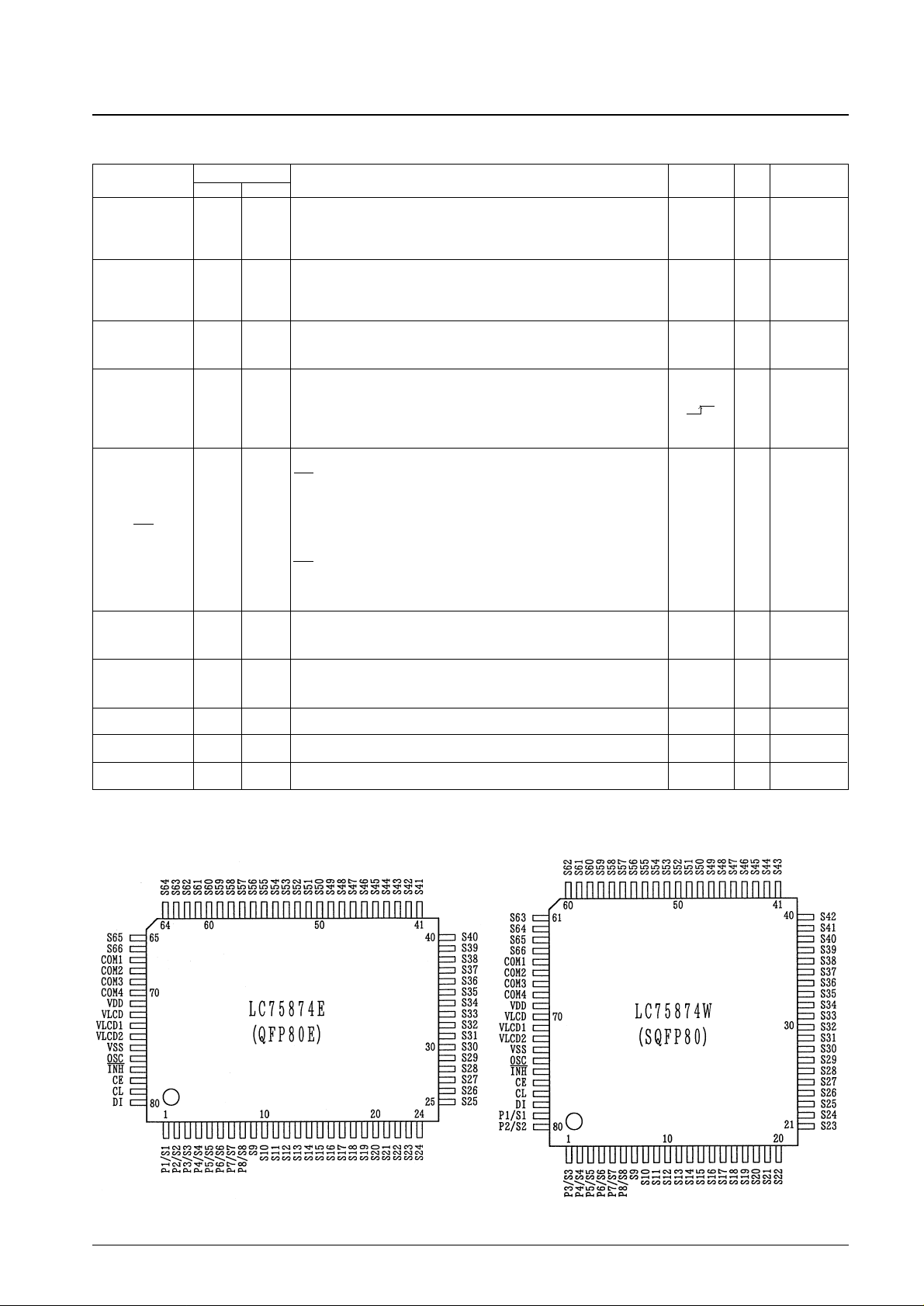
Package Dimensions
unit: mm
3174-QFP80E
unit: mm
3220-SQFP80
CMOS LSI
Ordering number : EN5800
31398RM (OT) No. 5800-1/16
SANYO Electric Co.,Ltd. Semiconductor Bussiness Headquarters
TOKYO OFFICE Tokyo Bldg., 1-10, 1 Chome, Ueno, Taito-ku, TOKYO, 110-8534 JAPAN
LC75874E, 75874W
1/4-Duty General-Purpose LCD Display Driver
[LC75874E]
SANYO: QFP80E
[LC75874W]
SANYO: SQFP80
• CCB is a trademark of SANYO ELECTRIC CO., LTD.
• CCB is SANYO’s original bus format and all the bus
addresses are controlled by SANYO.
Page 2
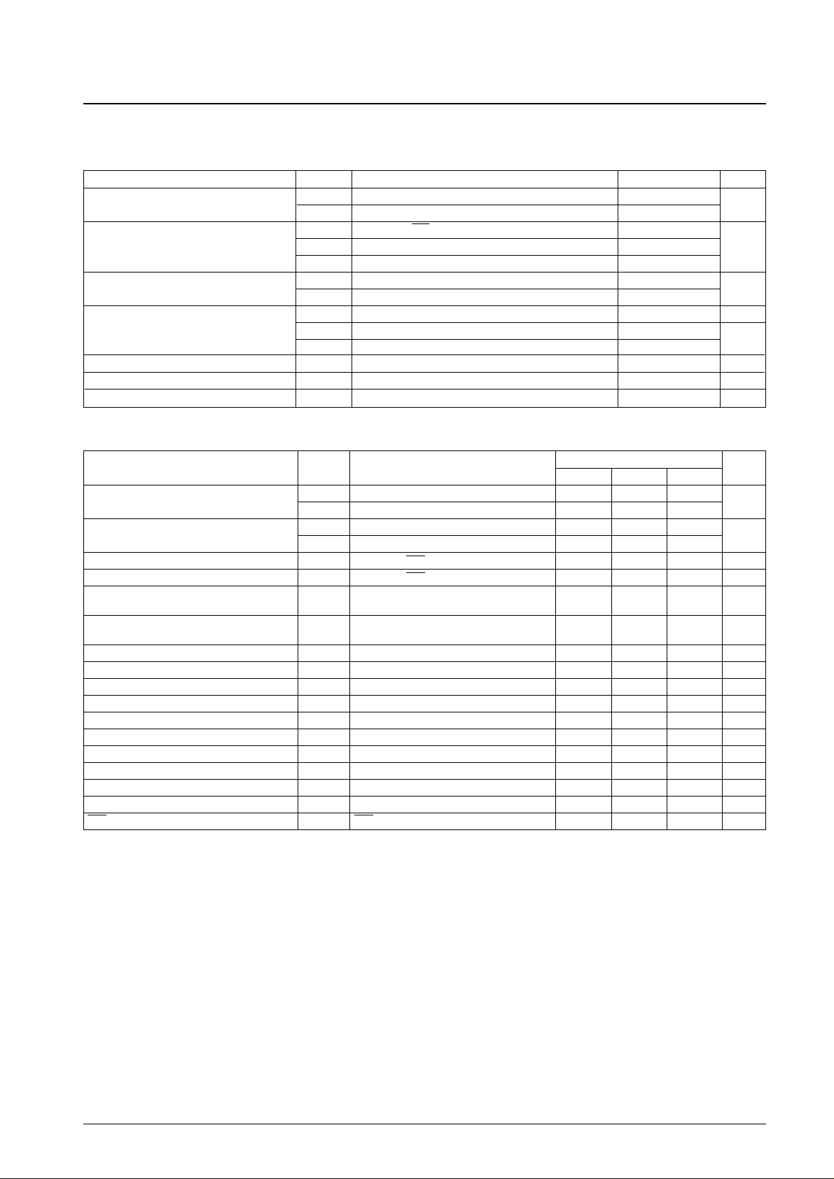
Specifications
Absolute Maximum Ratings at Ta = 25°C, VSS= 0 V
No. 4465-No. 5800-2/16
LC75874E, 75874W
Parameter Symbol Conditions Ratings Unit
Maximum supply voltage
V
DD
max V
DD
–0.3 to +7.0
V
V
LCD
max V
LCD
–0.3 to +7.0
V
IN
1 CE, CL, DI, INH –0.3 to +7.0
Input voltage V
IN
2 OSC –0.3 to VDD+ 0.3 V
V
IN
3 V
LCD
1, V
LCD
2 –0.3 to V
LCD
+ 0.3
Output voltage
V
OUT
1 OSC –0.3 to V
DD
+ 0.3
V
V
OUT
2 S1 to S66, COM1 to COM4, P1 to P8 –0.3 to V
LCD
+ 0.3
I
OUT
1 S1 to S66 300 µA
Output current I
OUT
2 COM1 to COM4 3
mA
I
OUT
3 P1 to P8 5
Allowable power dissipation Pd max Ta = 85°C 200 mW
Operating temperature Topr –40 to +85 °C
Storage temperature Tstg –55 to +125 °C
Parameter Symbol Conditions
Ratings
Unit
min typ max
Supply voltage
V
DD
V
DD
2.7 6.0
V
V
LCDVLCD
2.7 6.0
Input voltage
V
LCD
1 V
LCD
1 2/3 V
LCD
V
LCD
V
V
LCD
2 V
LCD
2 1/3 V
LCD
V
LCD
Input high-level voltage V
IH
CE, CL, DI, INH 0.8 V
DD
6.0 V
Input low-level voltage V
IL
CE, CL, DI, INH 0 0.2 V
DD
V
Recommended external
R
OSC
OSC 43 kΩ
resistance
Recommended external
C
OSC
OSC 680 pF
capacitance
Guaranteed oscillation range f
OSC
OSC 25 50 100 kHz
Data setup time t
ds
CL, DI: Figure 2 160 ns
Data hold time t
dh
CL, DI: Figure 2 160 ns
CE wait time t
cp
CE, CL: Figure 2 160 ns
CE setup time t
cs
CE, CL: Figure 2 160 ns
CE hold time t
ch
CE, CL: Figure 2 160 ns
High-level clock pulse width t
øH
CL: Figure 2 160 ns
Low-level clock pulse width t
øL
CL: Figure 2 160 ns
Rise time t
r
CE, CL, DI: Figure 2 160 ns
Fall time t
f
CE, CL, DI: Figure 2 160 ns
INH switching time t
c
INH, CE: Figure 3 10 µs
Allowable Operating Ranges at Ta = –40 to +85°C, VSS= 0 V
Page 3

Note: *1 Excluding the bias voltage generation divider resistors built in the V
LCD
1 and V
LCD
2. (See Figure 1.)
No. 4465No. 5800-3/16
LC75874E, 75874W
Parameter Symbol Conditions
Ratings
Unit
min typ max
Hysteresis V
H
CE, CL, DI, INH 0.1 V
DD
V
Input high-level current I
IH
CE, CL, DI, INH: VI= 6.0 V 5.0 µA
Input low-level current I
IL
CE, CL, DI, INH: VI= 0 V –5.0 µA
V
OH
1 S1 to S66: IO= –20 µA V
LCD
– 0.9
Output high-level voltage V
OH
2 COM1 to COM4: IO= –100 µA V
LCD
– 0.9 V
V
OH
3 P1 to P8: IO= –1 mA V
LCD
– 0.9
V
OL
1 S1 to S66: IO= 20 µA 0.9
Output low-level voltage V
OL
2 COM1 to COM4: IO= 100 µA 0.9 V
V
OL
3 P1 to P8: IO= 1 mA 0.9
V
MID
1 COM1 to COM4: 1/2 bias, IO= ±100 µA
1/2 V
LCD
– 1/2 V
LCD
+
0.9 0.9
V
MID
2 S1 to S66: 1/3 bias, IO= ±20 µA
2/3 V
LCD
– 2/3 V
LCD
+
0.9 0.9
Output middle-level voltage*1 V
MID
3 S1 to S66: 1/3 bias, IO= ±20 µA
1/3 V
LCD
– 1/3 V
LCD
+
V
0.9 0.9
V
MID
4 COM1 to COM4: 1/3 bias, IO= ±100 µA
2/3 V
LCD
– 2/3 V
LCD
+
0.9 0.9
V
MID
5 COM1 to COM4: 1/3 bias, IO= ±100 µA
1/3 V
LCD
– 1/3 V
LCD
+
0.9 0.9
Oscillator frequency f
OSC
OSC: R
OSC
= 43 kΩ, C
OSC
= 680 pF 40 50 60 kHz
I
DD
1 V
DD
: Power-saving mode 5
I
DD
2 VDD: VDD= 6.0 V, outputs open, f
OSC
= 50 kHz 230 460
Current drain I
LCD
1 V
LCD
: Power-saving mode 5 µA
I
LCD
2 V
LCD
:
V
LCD
= 6.0 V, outputs open, 1/2 bias, f
OSC
= 50 kHz
200 400
I
LCD
3 V
LCD
:
V
LCD
= 6.0 V, outputs open, 1/3 bias, f
OSC
= 50 kHz
120 240
Electrical Characteristics for the Allowable Operating Ranges
Figure 1
V
LCD
V
LCD
1
V
LCD
2
Page 4

1. When CL is stopped at the low level
2. When CL is stopped at the high level
Figure 2
Block Diagram
No. 4465-No. 5800-4/16
LC75874E, 75874W
Page 5
Pin Functions
No. 4465No. 5800-5/16
LC75874E, 75874W
Symbol
Pin No.
Function Active I/O
Handling
LC75874ELC75874W
when unused
1 to 8
9 to 66
79, 80,
1 to 6
7 to 64
67
68
69
70
65
66
67
68
76
74
78
76
79
80
78
77
77
75
73
71
74
72
71
69
72
70
S1/P1 to S8/P8
S9 to S66
COM1
COM2
COM3
COM4
OSC
CE
CL
DI
INH
V
LCD
1
V
LCD
2
V
DD
V
LCD
Segments outputs for displaying the display data transferred by serial data
input. The S1/P1 to S8/P8 pins can be used as general-purpose output
ports under serial data control.
Common driver outputs. The frame frequency fo is f
OSC
/512 Hz.
Oscillator connection. An oscillator circuit can be formed by connecting an
external resistor and capacitor at this pin.
Serial data transfer inputs. Connected to the controller.
CE: Chip enable
CL: Synchronization clock
DI: Transfer data
Display off control input
INH = low (V
SS
)......Display forced off
S1/P1 to S8/P8 = low (V
SS
)
(These pins are forcibly set to the segment output port
function and held at the V
SS
level.)
S9 to S66 = low (V
SS
)
COM1 to COM4 = low (V
SS
)
INH = high (V
DD
).....Display on
However, serial data transfer is possible when the display is forced off by
this pin.
Used to apply the LCD drive 2/3 bias voltage externally. Connect this pin to
V
LCD
2 when using a 1/2-bias drive scheme.
Used to apply the LCD drive 1/3 bias voltage externally. Connect this pin to
V
LCD
1 when using a 1/2-bias drive scheme.
Logic block power supply. In the range 2.7 to 6.0 V.
LCD driver block power supply. In the range 2.7 to 6.0 V.
—
—
—
H
—
L
—
—
—
—
O
O
I/O
I
I
I
I
I
I
—
—
Open
Open
V
DD
GND
GND
Open
Open
—
—
75
73
V
SS
Ground pin. Connect to ground. — — —
Pin Assignments
Top view
Page 6

Serial Data Transfer Format
1. When CL is stopped at the low level
Note: DD is the direction data.
No. 4465-No. 5800-6/16
LC75874E, 75874W
CCB address
8 bits
Display data
68 bits
DD
CCB address
8 bits
Display data
68 bits
Fixed data
10 bits
2 bits
DD
2 bits
DD
2 bits
DD
2 bits
Fixed data
14 bits
Fixed data
14 bits
Display data
64 bits
Display data
64 bits
CCB address
8 bits
CCB address
8 bits
Control data
10 bits
Page 7

2. When CL is stopped at the high level
Note: DD is the direction data.
• CCB address......45H
• D1 to D264........Display data
• P0 to P3.............Segment output port/general-purpose output port switching control data
• DR.....................1/2-bias drive or 1/3-bias drive switching control data
• SC......................Segments on/off control data
• BU.....................Normal mode/power-saving mode control data
No. 4465-No. 5800-7/16
LC75874E, 75874W
CCB address
8 bits
CCB address
8 bits
CCB address
8 bits
CCB address
8 bits
Display data
68 bits
Display data
68 bits
Display data
64 bits
Display data
64 bits
Control data
10 bits
Control data
10 bits
Control data
14 bits
Control data
14 bits
DD
2 bits
DD
2 bits
DD
2 bits
DD
2 bits
Page 8

Serial Data Transfer Example
1. When 201 or more segments are used
All 320 bits of serial data must be sent.
2. When fewer than 201 segments are used
Either 80, 160 or 240 bits of serial data may be sent, depending on the number of segments used. However, the serial
data shown below (the D1 to D68 display data and the control data) must be sent.
Control Data Functions
1. P0 to P3: Segment output port/general-purpose output port switching control data
These control data bits switch the segment output port/general-purpose output port functions of the S1/P1 to S8/P8
output pins.
Note: Sn (n = 1 to 8): Segment output port function
Pn (n = 1 to 8): General-purpose output port function
Note that when the general-purpose output port function is selected, the correspondence between the output pins and
the display data will be that shown in the table.
For example, if the general-purpose output port function is selected for the S4/P4 output pin, that output pin will
output a high level (V
LCD
) when the display data D13 is 1, and a low level (VSS) when the D13 is 0.
No. 4465-No. 5800-8/16
LC75874E, 75874W
Control data Output pin state
P0 P1 P2 P3 S1/P1 S2/P2 S3/P3 S4/P4 S5/P5 S6/P6 S7/P7 S8/P8
0 0 0 0 S1 S2 S3 S4 S5 S6 S7 S8
0 0 0 1 P1 S2 S3 S4 S5 S6 S7 S8
0 0 1 0 P1 P2 S3 S4 S5 S6 S7 S8
0 0 1 1 P1 P2 P3 S4 S5 S6 S7 S8
0 1 0 0 P1 P2 P3 P4 S5 S6 S7 S8
0 1 0 1 P1 P2 P3 P4 P5 S6 S7 S8
0 1 1 0 P1 P2 P3 P4 P5 P6 S7 S8
0 1 1 1 P1 P2 P3 P4 P5 P6 P7 S8
1 0 0 0 P1 P2 P3 P4 P5 P6 P7 P8
Output pin Corresponding display data
S1/P1 D1
S2/P2 D5
S3/P3 D9
S4/P4 D13
Output pin Corresponding display data
S5/P5 D17
S6/P6 D21
S7/P7 D25
S8/P8 D29
8 bits
80 bits
80 bits
8 bits
Page 9

2. DR: 1/2-bias drive or 1/3-bias drive switching control data
This control data bit selects either 1/2-bias drive or 1/3-bias drive.
3. SC: Segment on/off control data
This control data controls the on/off state of the segments.
Note that when the segments are turned off by setting SC to 1, the segments are turned off by outputting segment off
waveforms from the segment output pins.
4. BU: Normal mode/power-saving mode control data
This control data bit selects either normal mode or power-saving mode.
No. 4465-No. 5800-9/16
LC75874E, 75874W
SC Display state
0 On
1 Off
BU Mode
0 Normal mode
Power saving mode. In this mode, the OSC pin oscillator is stopped and the common and segment output pins go to the V
SS
level.
1
However, the S1/P1 to S8/P8 output pins can be used as general-purpose output ports under the control of the data bits P0 to P3.
DR Drive scheme
0 1/3-bias drive
1 1/2-bias drive
Page 10

Display Data and Output Pin Correspondence
Note: This table assumes that the segment output port function is selected for the S1/P1 to S8/P8 output pins.
For example, the table below lists the output states for the S11 output pin.
No. 4465-No. 5800-10/16
LC75874E, 75874W
Output pin COM1 COM2 COM3 COM4
S1/P1 D1 D2 D3 D4
S2/P2 D5 D6 D7 D8
S3/P3 D9 D10 D11 D12
S4/P4 D13 D14 D15 D16
S5/P5 D17 D18 D19 D20
S6/P6 D21 D22 D23 D24
S7/P7 D25 D26 D27 D28
S8/P8 D29 D30 D31 D32
S9 D33 D34 D35 D36
S10 D37 D38 D39 D40
S11 D41 D42 D43 D44
S12 D45 D46 D47 D48
S13 D49 D50 D51 D52
S14 D53 D54 D55 D56
S15 D57 D58 D59 D60
S16 D61 D62 D63 D64
S17 D65 D66 D67 D68
S18 D69 D70 D71 D72
S19 D73 D74 D75 D76
S20 D77 D78 D79 D80
S21 D81 D82 D83 D84
S22 D85 D86 D87 D88
S23 D89 D90 D91 D92
S24 D93 D94 D95 D96
S25 D97 D98 D99 D100
S26 D101 D102 D103 D104
S27 D105 D106 D107 D108
S28 D109 D110 D111 D112
S29 D113 D114 D115 D116
S30 D117 D118 D119 D120
S31 D121 D122 D123 D124
S32 D125 D126 D127 D128
S33 D129 D130 D131 D132
Display data
Output pin (S11) state
D41 D42 D43 D44
0 0 0 0 The LCD segments corresponding to COM1, COM2, COM3, and COM4 are off.
0 0 0 1 The LCD segments corresponding to COM4 are on.
0 0 1 0 The LCD segments corresponding to COM3 are on.
0 0 1 1 The LCD segments corresponding to COM3 and COM4 are on.
0 1 0 0 The LCD segments corresponding to COM2 are on.
0 1 0 1 The LCD segments corresponding to COM2 and COM4 are on.
0 1 1 0 The LCD segments corresponding to COM2 and COM3 are on.
0 1 1 1 The LCD segments corresponding to COM2, COM3, and COM4 are on.
1 0 0 0 The LCD segments corresponding to COM1 are on.
1 0 0 1 The LCD segments corresponding to COM1 and COM4 are on.
1 0 1 0 The LCD segments corresponding to COM1 and COM3 are on.
1 0 1 1 The LCD segments corresponding to COM1, COM3, and COM4 are on.
1 1 0 0 The LCD segments corresponding to COM1 and COM2 are on.
1 1 0 1 The LCD segments corresponding to COM1, COM2, and COM4 are on.
1 1 1 0 The LCD segments corresponding to COM1, COM2, and COM3 are on.
1 1 1 1 The LCD segments corresponding to COM1, COM2, COM3, and COM4 are on.
Output pin COM1 COM2 COM3 COM4
S34 D133 D134 D135 D136
S35 D137 D138 D139 D140
S36 D141 D142 D143 D144
S37 D145 D146 D147 D148
S38 D149 D150 D151 D152
S39 D153 D154 D155 D156
S40 D157 D158 D159 D160
S41 D161 D162 D163 D164
S42 D165 D166 D167 D168
S43 D169 D170 D171 D172
S44 D173 D174 D175 D176
S45 D177 D178 D179 D180
S46 D181 D182 D183 D184
S47 D185 D186 D187 D188
S48 D189 D190 D191 D192
S49 D193 D194 D195 D196
S50 D197 D198 D199 D200
S51 D201 D202 D203 D204
S52 D205 D206 D207 D208
S53 D209 D210 D211 D212
S54 D213 D214 D215 D216
S55 D217 D218 D219 D220
S56 D221 D222 D223 D224
S57 D225 D226 D227 D228
S58 D229 D230 D231 D232
S59 D233 D234 D235 D236
S60 D237 D238 D239 D240
S61 D241 D242 D243 D244
S62 D245 D246 D247 D248
S63 D249 D250 D251 D252
S64 D253 D254 D255 D256
S65 D257 D258 D259 D260
S66 D261 D262 D263 D264
Page 11

1/4-Duty 1/2-Bias Drive Scheme
1/4-Duty 1/2-Bias Waveforms
No. 4465-No. 5800-11/16
LC75874E, 75874W
COM1
COM2
COM3
COM4
LCD driver output when all LCD segments
corresponding to COM1, COM2, COM3, and
COM4 are off.
LCD driver output when only LCD segments
corresponding to COM1
are on (lit).
LCD driver output when only LCD segments
corresponding to COM2
are on.
LCD driver output when LCD
segments corresponding to COM1
and COM2 are on.
LCD driver output when only LCD segments
corresponding to COM3
are on.
LCD driver output when LCD
segments corresponding to COM1
and COM3 are on.
LCD driver output when LCD
segments corresponding to COM2
and COM3 are on.
LCD driver output when LCD segments
corresponding to COM1, COM2, and COM3
are on.
LCD driver output when only LCD segments
corresponding to COM4 are on.
LCD driver output when LCD segments
corresponding to COM2 and COM4 are on.
LCD driver output when all LCD segments
corresponding to COM1, COM2, COM3, and
COM4 are on.
Page 12

1/4-Duty 1/3-Bias Drive Scheme
1/4-Duty 1/3-Bias Waveforms
No. 4465-No. 5800-12/16
LC75874E, 75874W
COM1
COM2
COM3
COM4
LCD driver output when all LCD segments
corresponding to COM1, COM2, COM3, and
COM4 are off.
LCD driver output when only LCD segments
corresponding to COM1
are on (lit).
LCD driver output when only LCD segments
corresponding to COM2
are on.
LCD driver output when LCD
segments corresponding to COM1
and COM2 are on.
LCD driver output when only LCD segments
corresponding to COM3
are on.
LCD driver output when LCD
segments corresponding to COM1
and COM3 are on.
LCD driver output when LCD
segments corresponding to COM2
and COM3 are on.
LCD driver output when LCD segments
corresponding to COM1, COM2, and COM3
are on.
LCD driver output when only LCD segments
corresponding to COM4 are on.
LCD driver output when LCD segments
corresponding to COM2, and COM4 are on.
LCD driver output when all LCD segments
corresponding to COM1, COM2, COM3, and
COM4 are on.
Page 13

Display Control and the INH Pin
Since the LSI internal data (the display data D1 to D264 and the control data) is undefined when power is first applied,
applications should prevent meaningless displays with the following procedure. First, set the INH pin low at the same
time as power is applied to turn off the display. This will set the S1/P1 to S8/P8, S9 to S66, and COM1 to COM4 pins
low. While the INH pin is held low, the control microprocessor should send the serial data. Finally, the application can
set the INH pin to high. (See Figure 3.)
Notes on Power Supply Sequences
Applications must observe the following sequences when power is turned on or off.
• Power on: Turn on the logic power supply (VDD) first → then turn on the LCD driver power supply (V
LCD
).
• Power off: Turn off the LCD driver power supply (V
LCD
) first → then turn off the logic power supply (VDD).
However, if the logic and LCD driver block use a shared power supply, then the power supplies can be turned on and off
at the same time.
Figure 3
Notes on Controller Transfer of Display Data
Since the LC75874E and LC75874W accept the display data (D1 to D264) divided into four separate transfer operations,
we recommend that applications make a point of completing all four data transfers within a period of less than 30 ms to
prevent observable degradation of display quality.
No. 4465-No. 5800-13/16
LC75874E, 75874W
Internal data
(D1 to D68, P0 to P3, DR, SC, BU)
Internal data (D69 to D136)
Internal data (D137 to D200)
Internal data (D201 to D264)
Transfer of display and control data
Undefined
Undefined
Undefined
Undefined
Defined
Defined
Defined
Defined
Undefined
Undefined
Undefined
Undefined
Notes:
t1 ≥ 0
t2 > 0
t3 ≥ 0 (t2 > t3)
tc ....... 10 µs min.
Page 14

Sample Application Circuit 1
1/2 Bias (for normal LCD panels)
Sample Application Circuit 2
1/2 Bias (for large LCD panels)
No. 4465-No. 5800-14/16
LC75874E, 75874W
From the
controller
General-purpose
output ports
Used for functions
such as backlight
control
LCD panel
(up to 264 segments)
General-purpose
output ports
Used for functions
such as backlight
control
LCD panel
(up to 264 segments)
From the
controller
Note: *2 When a capacitor except the recommended external capacitance (Cosc = 680 pF) is connected the OSC pin, we recommend that applications
connect the OSC pin with a capacitor in the range 220 to 2200 pF.
Note: *2 When a capacitor except the recommended external capacitance (Cosc = 680 pF) is connected the OSC pin, we recommend that applications
connect the OSC pin with a capacitor in the range 220 to 2200 pF.
C ≥ 0.047 µF
10 kΩ ≥ R ≥ 1 kΩ
C ≥ 0.047 µF
*2
*2
Page 15

No. 4465-No. 5800-15/16
LC75874E, 75874W
Sample Application Circuit 3
1/3 Bias (for nornal LCD panels)
Sample Application Circuit 4
1/3 Bias (for large LCD panels)
From the
controller
From the
controller
General-purpose
output ports
General-purpose
output ports
Used for functions
such as backlight
control
Used for functions
such as backlight
control
LCD panel
(up to 264 segments)
LCD panel
(up to 264 segments)
Note: *2 When a capacitor except the recommended external capacitance (Cosc = 680 pF) is connected the OSC pin, we recommend that applications
connect the OSC pin with a capacitor in the range 220 to 2200 pF.
Note: *2 When a capacitor except the recommended external capacitance (Cosc = 680 pF) is connected the OSC pin, we recommend that applications
connect the OSC pin with a capacitor in the range 220 to 2200 pF.
10 kΩ ≥ R ≥ 1 kΩ
C ≥ 0.047 µF
C ≥ 0.047 µF
*2
*2
Page 16

PS No. 5800-16/16
LC75874E, 75874W
This catalog provides information as of March, 1998. Specifications and information herein are subject to
change without notice.
■ No products described or contained herein are intended for use in surgical implants, life-support systems, aerospace
equipment, nuclear power control systems, vehicles, disaster/crime-prevention equipment and the like, the failure of
which may directly or indirectly cause injury, death or property loss.
■ Anyone purchasing any products described or contained herein for an above-mentioned use shall:
➀ Accept full responsibility and indemnify and defend SANYO ELECTRIC CO., LTD., its affiliates, subsidiaries and
distributors and all their officers and employees, jointly and severally, against any and all claims and litigation and all
damages, cost and expenses associated with such use:
➁ Not impose any responsibility for any fault or negligence which may be cited in any such claim or litigation on
SANYO ELECTRIC CO., LTD., its affiliates, subsidiaries and distributors or any of their officers and employees
jointly or severally.
■ Information (including circuit diagrams and circuit parameters) herein is for example only; it is not guaranteed for
volume production. SANYO believes information herein is accurate and reliable, but no guarantees are made or implied
regarding its use or any infringements of intellectual property rights or other rights of third parties.
 Loading...