

Page 1
CMOS LSI
Ordering number : EN4828A
63096HA (OT)/N1594TH (OT) B8-1326, 1328 No. 4828-1/16
SANYO Electric Co.,Ltd. Semiconductor Bussiness Headquarters
TOKYO OFFICE Tokyo Bldg., 1-10, 1 Chome, Ueno, Taito-ku, TOKYO, 110 JAPAN
Asynchronous Silicon Gate 1/2 Duty LCD Driver
with On-Chip Key Input Function
LC75852E, 75852W
Overview
The LC75852E and LC75852W are 1/2 duty dynamic
LCD display drivers. In addition to being able to directly
drive LCD panels with up to 90 segments, they can also
control up to four general-purpose output ports. These
products also include a key scan circuit which allows
them to accept input from keypads with up to 30 keys.
This allows end product front panel wiring to be
simplified.
Features
• Up to 30 key inputs (Key scan is only performed when a
key is pressed.)
• 1/2 duty – 1/2 bias (up to 90 segments)
• Sleep mode and the all segments off function can be
controlled from serial data.
• Segment output port/general-purpose output port usage
can be controlled from serial data.
• Serial data I/O supports CCB format communication
with the system controller.
• High generality since display data is displayed directly
without decoder intervention
• Reset pin that can establish the initial state.
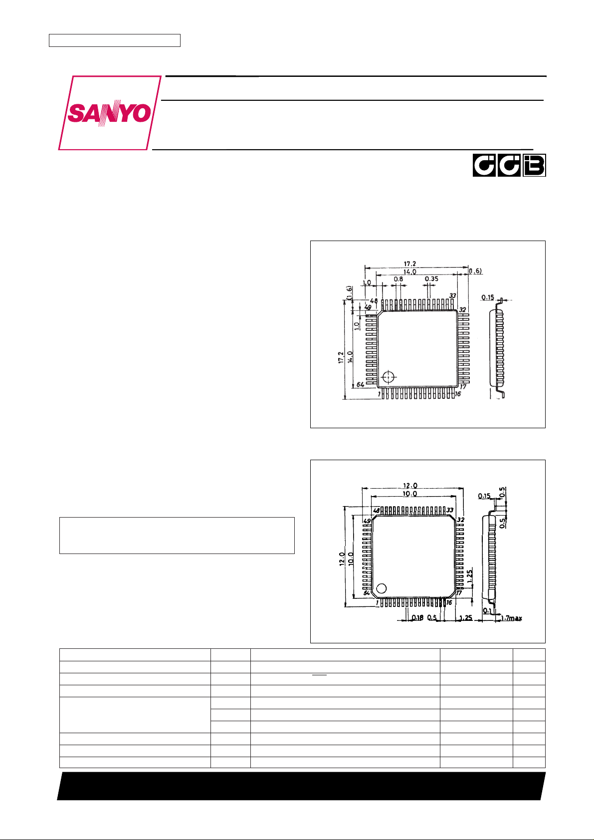
Package Dimensions
unit: mm
3159-QFP64E
unit: mm
3190-SQFP64
Specifications
Absolute Maximum Ratings at Ta = 25°C, VSS= 0 V
Parameter Symbol Conditions Ratings Unit
Maximum supply voltage V
DD
max V
DD
–0.3 to +7.0 V
Input voltage V
IN
OSC, CE, CL, DI, RES, KI1 to KI5 –0.3 to VDD+ 0.3 V
Output voltage V
OUT
OSC, DO, S1 to S45, COM1, COM2, KS1 to KS6, P1 to P4 –0.3 to VDD+ 0.3 V
I
OUT
1 S1 to S45 100 µA
Output current I
OUT
2 COM1, COM2, KS1 to KS6 1 mA
I
OUT
3 P1 to P4 5 mA
Allowable power dissipation Pd max Ta = 85°C 200 mW
Operating temperature Topr –40 to +85 °C
Storage temperature Tstg –55 to +125 °C
• CCB is a trademark of SANYO ELECTRIC CO., LTD.
• CCB is SANYO’s original bus format and all the bus
addresses are controlled by SANYO.
[LC75852E]
SANYO: QIP64E
SANYO: SQFP64
[LC75852W]
Page 2
Allowable Operating Ranges at Ta = –40 to +85°C, VSS= 0 V
Note: * Since DO is an open-drain output, these values differ depending on the pull-up resistor RPUand the load capacitance CL.
Electrical Characteristics in the Allowable Operating Ranges
No. 4828-2/16
LC75852E, 75852W
Parameter Symbol Conditions min typ max Unit
Supply voltage V
DD
V
DD
4.5 6.0 V
Input high-level voltage
V
IH
1 CE, CL, DI, RES 0.8 V
DD
V
DD
V
V
IH
2 KI1 to KI5 0.6 V
DD
V
DD
V
Input low-level voltage V
IL
CE, CL, DI, RES, KI1 to KI5 0 0.2 V
DD
V
Recommended external
R
OSC
OSC 62 kΩ
resistance
Recommended external
C
OSC
OSC 680 pF
capacitance
Guaranteed oscillator range f
OSC
OSC 25 50 100 kHz
Data setup time t
ds
CL, DI: Figure 1 160 ns
Data hold time t
dh
CL, DI: Figure 1 160 ns
CE wait time t
cp
CE, CL: Figure 1 160 ns
CE setup time t
cs
CE, CL: Figure 1 160 ns
CE hold time t
ch
CE, CL: Figure 1 160 ns
High-level clock pulse width t
øH
CL: Figure 1 160 ns
Low-level clock pulse width t
øL
CL: Figure 1 160 ns
Rise time t
r
CE, CL, DI: Figure 1 160 ns
Fall time t
f
CE, CL, DI: Figure 1 160 ns
DO output delay time t
dc
DO, RPU= 4.7 kΩ, CL= 10 pF*: Figure 1 1.5 µs
DO rise time t
dr
DO, RPU= 4.7 kΩ, CL= 10 pF*: Figure 1 1.5 µs
RES switching time t2 Figure 2 10 µs
Parameter Symbol Conditions min typ max Unit
Hysteresis V
H
CE, CL, DI, RES, KI1 to KI5 0.1 V
DD
V
Input high-level current I
IH
CE, CL, DI, RES: VI= 6.0 V 5.0 µA
Input low-level current I
IL
CE, CL, DI, RES: VI= 0 V –5.0 µA
Input floating voltage V
IF
KI1 to KI5 0.05 V
DD
V
Pull-down resistance R
PD
KI1 to KI5: VDD= 5.0 V 50 100 250 kΩ
Output off leakage current I
OFFH
DO: VO= 6.0 V 6.0 µA
V
OH
1 KS1 to KS6: IO= –1 mA VDD– 1.0 V
Output high-level voltage
V
OH
2 P1 to P4: IO= –1 mA VDD– 1.0 V
V
OH
3 S1 to S45: IO= –10 µA VDD– 1.0 V
V
OH
4 COM1, COM2: IO= –100 µA VDD– 0.6 V
V
OL
1 KS1 to KS6: IO= 50 µA 0.4 1.0 3.0 V
V
OL
2 P1 to P4: IO= 1 mA 1.0 V
Output low-level voltage V
OL
3 S1 to S45: IO= 10 µA 1.0 V
V
OL
4 COM1, COM2: IO= 100 µA 0.6 V
V
OL
5 DO: IO= 1 mA 0.1 0.5 V
Output middle-level voltage
V
MID
1 COM1, COM2: VDD= 6.0 V, IO= ±100 µA 2.4 3.0 3.6 V
V
MID
2 COM1, COM2: VDD= 4.5 V, IO= ±100 µA 1.65 2.25 2.85 V
Current drain
I
DD
1 Sleep mode, Ta = 25°C 5 µA
I
DD
2 VDD= 6.0 V, output open, Ta = 25°C, f
OSC
= 50 kHz 1.4 2.5 mA
Page 3
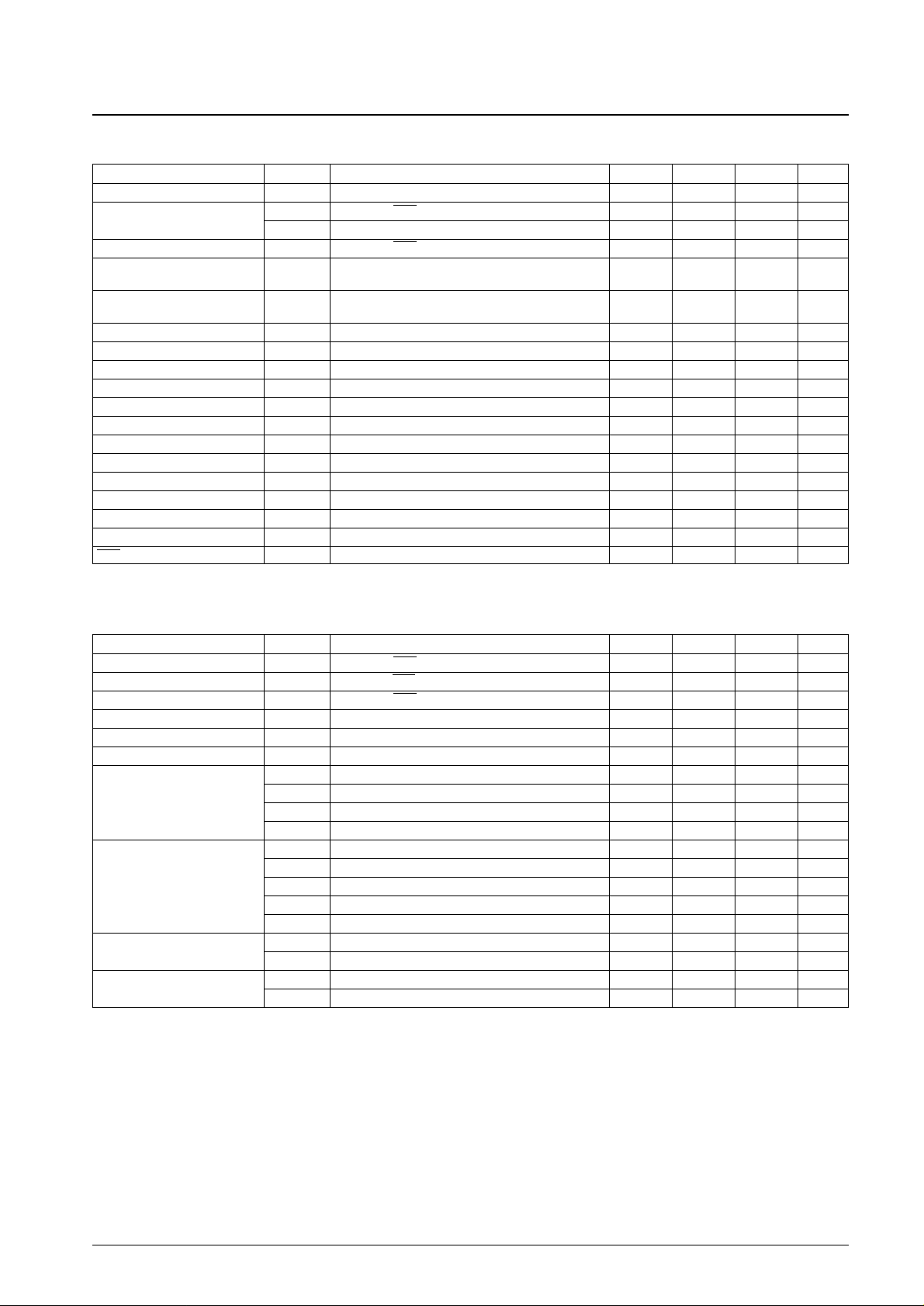
1. When stopped with CL at the low level
2. When stopped with CL at the high level
Figure 1
Pin Assignment
No. 4828-3/16
LC75852E, 75852W
Page 4
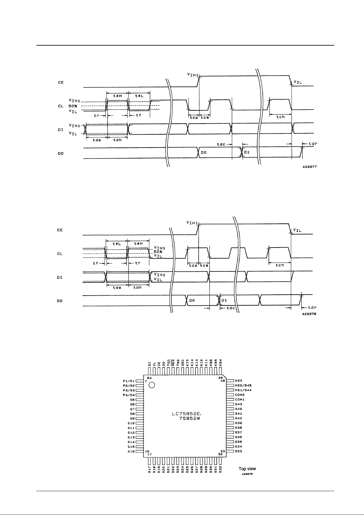
Block Diagram
Pin Functions
No. 4828-4/16
LC75852E, 75852W
Pin Pin No. Function Active I/O
Handling when
unused
S1/P1 to S4/P4
S5 to S43
COM1
COM2
KS1/S44,
KS2/S45,
KS3 to KS6
KI1 to KI5
OSC
CE
CL
DI
DO
RES
V
DD
V
SS
1 to 4
5 to 43
44
45
46
47
48 to 51
52 to 56
57
62
63
64
61
59
60
58
Segment outputs: Used to output the display data that is transmitted over the
serial data input. Pins S1/P1 to S4/P4 can be used as general-purpose outputs
according to control data specification.
Common driver outputs. The frame frequency f
O
is (f
OSC
/512) Hz.
Key scan outputs. When a key matrix is formed, normally a diode will be
attached to the key scan timing line to prevent shorts. However, since the
output transistor impedance is an unbalanced CMOS output, it will not be
damaged if shorted. Pins KS1/S44 and KS2/S45 can be used as segment
outputs according to control data specification.
Key scan inputs: Pins with a built-in pull-down resistor.
Oscillator connection: Oscillator circuit can be formed by connecting the pin to
a resistor and a capacitor.
CE: Chip enable
CL: Synchronization clock
DI: Transfer data
DO: Output data
Serial data interface: Connected
to the controller. Since DO is an
open-drain output, it requires a
pull-up resistor.
Reset input that re-initializes the LSI internal states. During a reset, the display
segments are turned off forcibly regardless of the internal display data. All
internal key data is reset to low and the key scan operation is disabled.
However, serial data can be input during a reset.
Power supply connection. A supply voltage of between 4.5 and 6.0 V must be
provided.
Power supply ground connection. Must be connected to GND.
—
—
—
H
—
H
—
—
L
—
—
O
O
O
I
I/O
I
I
I
O
I
—
—
Open
Open
Open
GND
V
DD
GND
Open
GND
—
—
Page 5
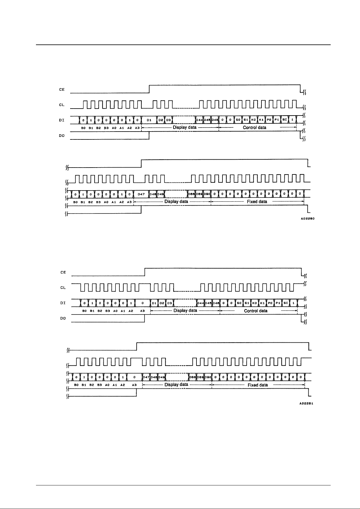
Serial Data Input
1. When stopped with CL at the low level
2. When stopped with CL at the high level
CCB address......................[42H]
D1 to D90...........................Display data
S0, S1 ................................Sleep control data
K0, K1 ................................Key scan output/segment output selection data
P0, P1 ................................Segment output port/general-purpose output port selection data
SC......................................Segment on/off control data
No. 4828-5/16
LC75852E, 75852W
Page 6

Control Data Functions
1. S0, S1.................Sleep control data
This control data switches the LSI between normal mode and sleep mode. It also sets the key scan output standby
states for pins KS1 to KS6.
Note: The KS1/S44 and KS2/S45 output pins are set to the key scan output state.
2. K0, K1................Key scan output/segment output selection data
This control data switches the KS1/S44 and KS2/S45 output pins between the key scan output and segment output
functions.
X: don’t care
3. P0, P1.................Segment output port/general-purpose output port selection data
This control data switches the S1/P1 to S4/P4 output pins between the segment output port and the general-purpose
output port functions.
The table below lists the correspondence between the display data and the output pins when the general-purpose
output port function is selected.
For example, if the output pin S4/P4 is set for use as a general-purpose output port, the output pin S4/P4 will output a
high level when the display data D7 is 1.
4. SC.......................Segment on/off control data
This control data controls the segment on/off states.
No. 4828-6/16
LC75852E, 75852W
Control data
Mode Oscillator
Segment outputs
Key scan standby mode output pin states
S0 S1
Common outputs
KS1 KS2 KS3 KS4 KS5 KS6
0 0 Normal Oscillator Operation H H H H H H
0 1 Sleep Stopped L L L L L L H
1 0 Sleep Stopped L L L L L H H
1 1 Sleep Stopped L H H H H H H
Control data Output pin states
Maximum number
K0 K1 KS1/S44 KS2/S45
of key inputs
0 0 KS1 KS2 30
0 1 S44 KS2 25
1 X S44 S45 20
Control data Output pin states
P0 P1 S1/P1 S2/P2 S3/P3 S4/P4
0 0 S1 S2 S3 S4
0 1 P1 P2 S3 S4
1 0 P1 P2 P3 S4
1 1 P1 P2 P3 P4
Output Corresponding
pin display data
S1/P1 D1
S2/P2 D3
S3/P3 D5
S4/P4 D7
SC Display state
0 On
1 Off
Page 7

Display Data and Output Pin Correspondences
For example, the output states of output pin S11 are listed in the table below.
No. 4828-7/16
LC75852E, 75852W
Output pin COM1 COM2
S1/P1 D1 D2
S2/P2 D3 D4
S3/P3 D5 D6
S4/P4 D7 D8
S5 D9 D10
S6 D11 D12
S7 D13 D14
S8 D15 D16
S9 D17 D18
S10 D19 D20
S11 D21 D22
S12 D23 D24
S13 D25 D26
S14 D27 D28
S15 D29 D30
S16 D31 D32
S17 D33 D34
S18 D35 D36
S19 D37 D38
S20 D39 D40
S21 D41 D42
S22 D43 D44
S23 D45 D46
S24 D47 D48
S25 D49 D50
S26 D51 D52
S27 D53 D54
S28 D55 D56
S29 D57 D58
S30 D59 D60
S31 D61 D62
S32 D63 D64
S33 D65 D66
S34 D67 D68
S35 D69 D70
S36 D71 D72
S37 D73 D74
S38 D75 D76
S39 D77 D78
S40 D79 D80
S41 D81 D82
S42 D83 D84
S43 D85 D86
KS1/S44 D87 D88
KS2/S45 D89 D90
Display data Output pin state
D21 D22 S11
0 0 Segment off for both COM1 and COM2
0 1 Segment on for COM2
1 0 Segment on for COM1
1 1 Segments on for both COM1 and COM2
Page 8

Serial Data Output
1. When stopped with CL at the low level
2. When stopped with CL at the high level
CCB address......................[43H]
KD1 to KD30......................Key data
SA ......................................Sleep acknowledge data
Note: If key data is read when DO is high, the key data (KD1 to KD30) and sleep acknowledge data (SA) will be
invalid.
Output Data
1. KD1 to KD30.....Key data
When a key matrix with up to 30 keys is formed using the KS1 to KS6 output pins and the KI1 to KI5 input pins, the
key data corresponding to a given key will be 1 if that key is pressed. The table below lists that correspondence.
When the output pins KS1/S44 and KS2/S45 are selected for segment output by the control data K0 and K1, the key
data items KD1 to KD10 will be 0.
2. SA ......................Sleep acknowledge data
This output data is set according to the state when the key was pressed. If the LSI was in sleep mode, SA will be 1,
and if the LSI was in normal mode, SA will be 0.
Sleep Mode
When S0 or S1 in the control data is set to 1, the oscillator at the OSC pin will stop (it will restart if a key is pressed) and
the segment and common outputs will all go to the low level. This reduces the LSI power dissipation. However, the
S1/P1 to S4/P4 output pins can be used as general-purpose output ports even in sleep mode if selected for such use by
the P0 and P1 control data bits.
No. 4828-8/16
LC75852E, 75852W
Item KI1 KI2 KI3 KI4 KI5
KS1/S44 KD1 KD2 KD3 KD4 KD5
KS2/S45 KD6 KD7 KD8 KD9 KD10
KS3 KD11 KD12 KD13 KD14 KD15
KS4 KD16 KD17 KD18 KD19 KD20
KS5 KD21 KD22 KD23 KD24 KD25
KS6 KD26 KD27 KD28 KD29 KD30
Page 9

Key Scan Operation
1. Key Scan Timing
The key scan period is 375T [s]. The key scan is performed twice to reliably determine the key on/off states, and the
LSI detects key data agreement. When the key data agrees, the LSI determines that a key has been pressed, and outputs
a key read request (by setting DO low) 800T [s] after the key scan started. If a key is pressed again without the key data
agreeing, a key scan is performed once more. Thus key on/off operations shorter than 800T [s] cannot be detected.
*1 The high or low states of these signals in sleep mode are determined by the S0 and S1 control data bits.
2. Key Scan during Normal Mode
• The pins KS1 to KS6 are set high.
• A key scan starts if any key is pressed, and the scan continues until all keys have been released. Multiple key
presses can be recognized by determining if multiple key data bits have been set.
• When a key has been pressed for 800T [s] (where T = 1/f
OSC
) or longer, a key data read request (DO is set to low)
is output to the controller. The controller acknowledges this request and reads the key data. However, DO will go
high when CE is high during a serial data transfer.
• After the controller has finished reading the key data, the LSI clears the key data read request (by setting DO high)
and performs another key scan. Note that since DO is an open drain output, a pull-up resistor of between 1 and 10 kΩ
is required.
No. 4828-9/16
LC75852E, 75852W
Page 10

3. Key Scan during Sleep Mode
• The pins KS1 to KS6 are set high or low according to the S0 and S1 control data bits.
(See the description of the control data function for details.)
• If a key for a line corresponding to one of the pins KS1 to KS6 which is high is pressed, the oscillator at the OSC
pin starts and a key scan is performed. The key scan continues until all keys have been released. Multiple key
presses can be recognized by determining if multiple key data bits have been set.
• When a key has been pressed for 800T [s] (where T = 1/f
OSC
) or longer, a key data read request (DO is set to low)
is output to the controller. The controller acknowledges this request and reads the key data. However, DO will go
high when CE is high during a serial data transfer.
• After the controller has finished reading the key data, the LSI clears the key data read request (by setting DO high)
and performs another key scan. Note that since DO is an open drain output, a pull-up resistor of between 1 and 10 kΩ
is required.
• Key scan example in sleep mode
Example: Here S0 = 0 and S1 = 1 (This is a sleep in which only KS6 is high.)
Multiple Key Presses
Without the insertion of additional diodes, the LC75852 supports key scan for double key presses in general, triple key
presses of keys on the lines for input pins KI1 to KI5, and multiple key presses of keys on the lines for the output pins
KS1 to KS6. However, if multiple key presses in excess of these limits occur, the LC75852 may recognize keys that
were not pressed as having been pressed. Therefore, series diodes must be connected to each key.
No. 4828-10/16
LC75852E, 75852W
Page 11

1/2 Duty - 1/2 Bias LCD Drive Scheme
RES and the Display Controller
Since the LSI internal data (D1 to D90 and the control data) is undefined when power is first applied, the output pins
S1/P1 to S4/P4, S5 to S43, COM1, COM2, KS1/S44 and KS2/S45 should be held low by setting the RES pin low at the
same time as power is applied. Then, meaningless displays at power on can be prevented by transferring data from the
controller and setting RES high when that transfer has completed.
Figure 2
No. 4828-11/16
LC75852E, 75852W
COM1
COM2
S1 to S45 outputs for segments on
COM1 side being lit
S1 to S45 outputs for segments on
COM2 side being lit
S1 to S45 outputs for segments on
COM1,COM2 sides being lit
S1 to S45 outputs for segments on
COM1,COM2 sides not being lit
Page 12

Internal Block States during the Reset Period (when RES is low)
1. CLOCK GENERATOR
Reset is applied and the basic clock stops. However, the state of the OSC pin (the normal or sleep state) is
determined after the control data S0 and S1 has been sent.
2. COMMON DRIVER, SEGMENT DRIVER & LATCH
Reset is applied and the display is turned off. However, display data can be input to the LATCH.
3. KEY SCAN
Reset is applied and at the same time as the internal states are set to their initial states, the key scan operation is
disabled.
4. KEY BUFFER
Reset is applied and all the key data is set to the low level.
5. CCB INTERFACE, CONTROL REGISTER, SHIFT REGISTER
To allow serial data transfers, reset is not applied to these circuits.
X: don’t care
Note: 3. These output pins are forcibly set to the segment output mode and held low.
4. Immediately following power on, these output pins are undefined until the control data S0 and S1 has been sent.
5. Since this output pin is an open-drain output, a pull-up resistor of between 1 and 10 kΩ is required. This pin is held high during the reset period
even if key data is read.
No. 4828-12/16
LC75852E, 75852W
Output pin State during reset
S1/P1 to S4/P4 L
*3
S5 to S43 L
COM1, COM2 L
KS1/S44, KS2/S45 L
*3
KS3 to KS5 X
*4
KS6 H
DO H
*5
Output Pin States during the Reset Period (when RES is low)
Page 13

Sample Application Circuit
Note: * Since DO is an open-drain output, a pull-up resistor is required. Select a value (between 1 and 10 kΩ) that is appropriate for the capacitance of the
external wiring so that the waveforms are not distorted.
Notes on Controller Display Data Transfer
The LC75852 transfers the display data (D1 to D90) in two operations. To assure visual display quality, all the display
data should be sent within a 30 ms or shorter period.
No. 4828-13/16
LC75852E, 75852W
Page 14

Notes on Controller Key Data Read Techniques
1. Controller key data reading under timer control
• Flowchart
• Timing Chart
t3 ..................Key scan execution time (800T [s]) when the key scan data for two key scans agrees
t4 ..................Key scan execution time (1600T [s]) when the key scan data for two key scans does not agree and a key scan is executed again
t5 ..................Key address (43H) transfer time
t6 ..................Key data read time
T =
• Description
When determining key on/off and reading key data, the controller must confirm the state of DO output when CE is
low for each period t7. When DO is low, the controller recognizes that a key has been pressed and reads the key
data.
During this operation t7 must obey the following condition:
t7 > t5 + t6 + t4
If key data is read when DO is high, the key data (KD1 to KD30) and the sleep acknowledge data (SA) will be
invalid.
1
f
OSC
No. 4828-14/16
LC75852E, 75852W
Page 15

2. Controller key data reading under interrupt control
• Flowchart
• Timing Chart
t3 ..................Key scan execution time (800T [s]) when the key scan data for two key scans agrees
t4 ..................Key scan execution time (1600T [s]) when the key scan data for two key scans does not agree and a key scan is executed again
t5 ..................Key address (43H) transfer time
t6 ..................Key data read time
T =
1
f
OSC
No. 4828-15/16
LC75852E, 75852W
Page 16

No. 4828-16/16
LC75852E, 75852W
• Description
When determining key on/off and reading key data, the controller must confirm the state of DO output when CE is
low. When DO is low, the controller recognizes that a key has been pressed and reads the key data. After the time
t8, the next key on/off determination and reading key data must be confirmed by the state of DO output when CE is
low. During this operation t8 must obey the following condition:
t8 > t4
If key data is read when DO is high, the key data (KD1 to KD30) and the sleep acknowledge data (SA) will be
invalid.
This catalog provides information as of November, 1997. Specifications and information herein are subject to
change without notice.
■ No products described or contained herein are intended for use in surgical implants, life-support systems, aerospace
equipment, nuclear power control systems, vehicles, disaster/crime-prevention equipment and the like, the failure of
which may directly or indirectly cause injury, death or property loss.
■ Anyone purchasing any products described or contained herein for an above-mentioned use shall:
➀ Accept full responsibility and indemnify and defend SANYO ELECTRIC CO., LTD., its affiliates, subsidiaries and
distributors and all their officers and employees, jointly and severally, against any and all claims and litigation and all
damages, cost and expenses associated with such use:
➁ Not impose any responsibility for any fault or negligence which may be cited in any such claim or litigation on
SANYO ELECTRIC CO., LTD., its affiliates, subsidiaries and distributors or any of their officers and employees
jointly or severally.
■ Information (including circuit diagrams and circuit parameters) herein is for example only; it is not guaranteed for
volume production. SANYO believes information herein is accurate and reliable, but no guarantees are made or implied
regarding its use or any infringements of intellectual property rights or other rights of third parties.
 Loading...