

Page 1
Overview
The LC75842E is a 1/2 duty general-purpose LCD display
driver for applications such as microprocessor-controlled
electronic tuning. It can drive up to 54 segments directly.
Features
• 1/2 duty, 1/2 bias drive of up to 54 segments
• Serial data input supports CCB* format communication
with the system controller.
• Backup function which is based on a power saving
mode and all segments off functions that are controlled
by serial data.
• High generality, since display data is displayed directly
without decoder intervention.
• The display can be forced to the off state with the INH
pin.
• RC oscillator circuit
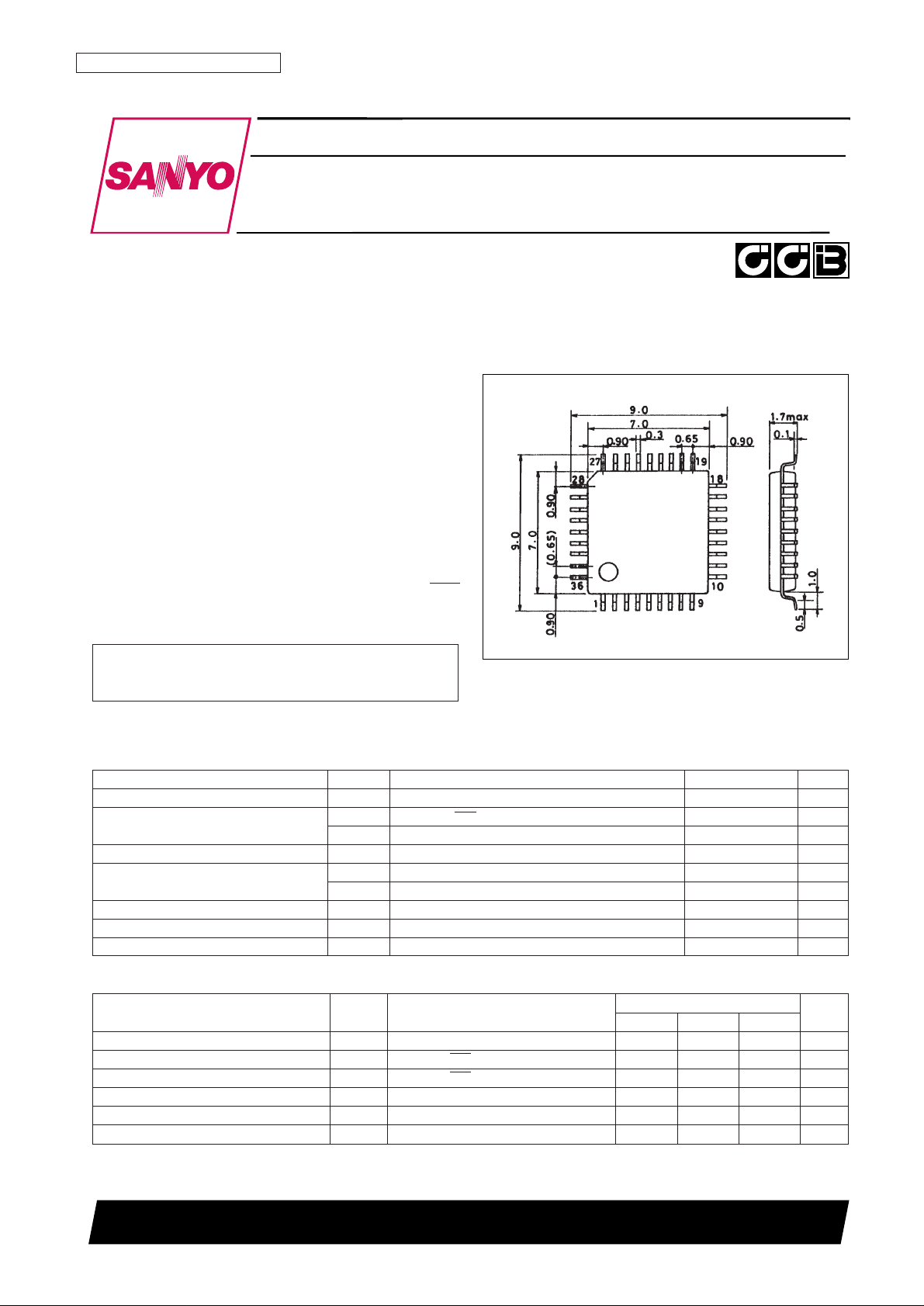
Package Dimensions
unit: mm
3162B-QFP36
CMOS LSI
41096HA (OT)/61595HA (OT) No. 4966-1/9
SANYO: QFP36
[LC75842E]
SANYO Electric Co.,Ltd. Semiconductor Bussiness Headquarters
TOKYO OFFICE Tokyo Bldg., 1-10, 1 Chome, Ueno, Taito-ku, TOKYO, 110 JAPAN
General-Purpose 1/2 Duty LCD Display Driver
LC75842E
Ordering number : EN4966A
• CCB is a trademark of SANYO ELECTRIC CO., LTD.
• CCB is SANYO’s original bus format and all the bus
addresses are controlled by SANYO.
Specifications
Absolute Maximum Ratings at Ta = 25°C, VSS= 0 V
Parameter Symbol Conditions Ratings Unit
Maximum supply voltage V
DD
max V
DD
–0.3 to +6.5 V
Input voltage
V
IN
1 CE, CL, DI, INH –0.3 to +6.5 V
V
IN
2 OSC –0.3 to VDD+ 0.3 V
Output voltage V
OUT
OSC, S1 to S27, COM1, COM2 –0.3 to VDD+ 0.3 V
Output current
I
OUT
1 S1 to S27 100 µA
I
OUT
2 COM1, COM2 1 mA
Allowable power dissipation Pd max Ta = 85°C 100 mW
Operating temperature Topr –40 to +85 °C
Storage temperature Tstg –55 to +125 °C
Parameter Symbol Conditions
Ratings
Unit
min typ max
Supply voltage V
DDVDD
* 4.0 5.0 6.0 V
Input high level voltage V
IH
CE, CL, DI, INH 0.8 V
DD
6.0 V
Input low level voltage V
IL
CE, CL, DI, INH 0 0.2 V
DD
V
Recommended external resistance R
OSC
OSC 68 kΩ
Recommended external capacitance C
OSC
OSC 680 pF
Guaranteed oscillator range f
OSC
OSC 25 50 100 kHz
Allowable Operating Ranges at Ta = –40 to +85°C, VSS= 0 V
Note: * Please contact your Sanyo sales representative if you need to operate the LC75842E at a power supply voltage VDDof 3.0 V (min.).
Continued on next page.
Page 2
No. 4966-2/9
LC75842E
Continued from preceding page.
Parameter Symbol Conditions
Ratings
Unit
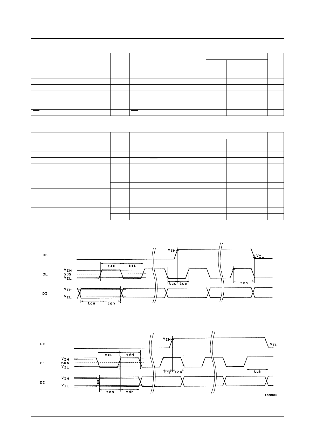
min typ max
Low level clock pulse width t
øL
CL: Figure 1 160 ns
High level clock pulse width t
øH
CL: Figure 1 160 ns
Data setup time t
ds
CL, DI: Figure 1 160 ns
Data hold time t
dh
CL, DI: Figure 1 160 ns
CE wait time t
cp
CE, CL: Figure 1 160 ns
CE setup time t
cs
CE, CL: Figure 1 160 ns
CE hold time t
ch
CE, CL: Figure 1 160 ns
INH switching time t
c
INH, CE: Figure 3 10 µs
Parameter Symbol Conditions
Ratings
Unit
min typ max
Hysteresis voltage V
H
CE, CL, DI, INH: VDD= 5.0 V 0.4 V
Input high level current I
IH
CE, CL, DI, INH: VI= 6.0 V 5.0 µA
Input low level current I
IL
CE, CL, DI, INH: VI= 0 V –5.0 µA
Output high level voltage
V
OH
1 S1 to S27: IO= –10 µA VDD– 1.0 V
V
OH
2 COM1, COM2: IO= –100 µA VDD– 0.6 V
Output low level voltage
V
OL
1 S1 to S27: IO= 10 µA 1.0 V
V
OL
2 COM1, COM2: IO= 100 µA 0.6 V
Output middle level voltage
V
MID
1 COM1, COM2: VDD= 6.0 V, IO= ±100 µA 2.4 3.0 3.6 V
V
MID
2 COM1, COM2: VDD= 4.0 V, IO= ±100 µA 1.4 2.0 2.6 V
Oscillator frequency f
OSC
OSC: R
OSC
= 68 kΩ, C
OSC
= 680 pF 40 50 60 kHz
Current drain
I
DD
1 Power saving mode 5 µA
I
DD
2 VDD= 6.0 V, output open, f
OSC
= 50 kHz 1.2 2.0 mA
Electrical Characteristics in the Allowable Operating Ranges
1. When CL is stopped at the low level
2. When CL is stopped at the high level
Figure 1
Page 3
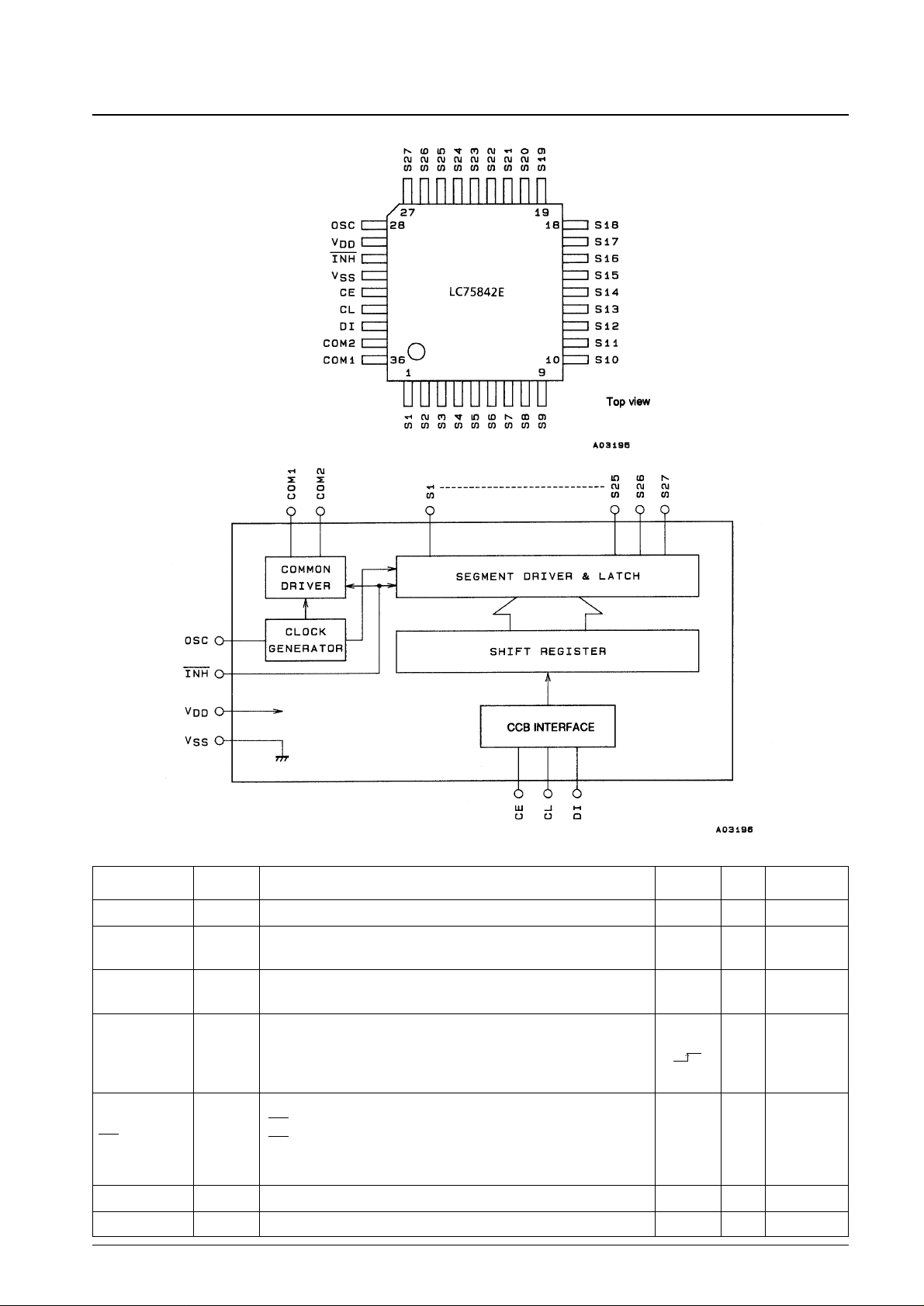
Pin Assignment
No. 4966-3/9
LC75842E
Block Diagram
Pin Pin No. Function Active I/O
Handling when
unused
S1 to S27
COM1
COM2
OSC
CE
CL
DI
INH
V
DD
V
SS
1 to 27
36
35
28
32
33
34
30
29
31
Segment outputs for displaying the display data transferred by serial data input.
Common driver outputs. The frame frequency f
O
is f
OSC
/512 Hz.
Oscillator connection. An oscillator circuit is formed by connecting an external
resistor and capacitor at this pin.
Serial data transfer inputs. Must be connected to the control microprocessor.
CE: Chip enable
CL: Synchronization clock
DI: Transfer data
Display off control input
INH = low (V
SS
).....Display off (S1 to S27, COM1 and COM2 = low)
INH = high (V
DD
)....Display on
However, serial data transfer is possible when the display is forced off by this
pin.
Power supply. Provide a power supply voltage of between 4.0 and 6.0 V.
Power supply. Connect this pin to ground.
—
—
—
L
—
—
H
—
O
O
I/O
I
I
—
—
Open
Open
V
DD
GND
GND
—
—
Pin Functions
Page 4

Serial Data Transfer Format
1. When CL is stopped at the low level
No. 4966-4/9
LC75842E
Page 5

2. When CL is stopped at the high level
Figure 2
• CCB address......44
H
• D1 to D54..........Display data
Dn (n = 1 to 54) = 1: Segment on
Dn (n = 1 to 54) = 0: Segment off
• BU.....................Control data for specifying normal mode or power saving mode
• SC......................Control data for specifying all segments on or off
Serial Data Transfer Example
When 29 or more segments are used all 80 bits of the serial data must be sent.
When fewer than 29 segments are used only the first 40 bits of the serial data can be sent. However, all 80 bits must be
sent after power is first applied.
Note: The following type of transfer cannot be used when fewer than 29 segments are used.
No. 4966-5/9
LC75842E
Page 6

Control Data Functions
1. BU: Control data for specifying normal mode or power saving mode
This control data bit is used to control the normal mode/power saving mode state of the LC75842E.
2. SC: Control data for specifying all segments on or off
This control data bit is used to turn all segments on or off.
Note that when SC is 1 the display is turned off by outputting the segment off waveforms from the segment pins.
Correspondence between Display Data and Segment Output Pins
For example, the table below lists the output states for the S11 segment output pin.
No. 4966-6/9
LC75842E
SC Display state
0 On
1 Off
BU Mode
0 Normal mode
1 Power saving mode (The OSC pin oscillator is stopped and the common and segment pins go to the V
SS
level.)
Display data
Segment output pin (S11) state
D21 D22
0 0 Both segments for COM1 and COM2 are off.
0 1 Segment for COM2 is on.
1 0 Segment for COM1 is on.
1 1 Both segments for COM1 and COM2 are on.
Segment
COM1 COM2
output pin
S1 D1 D2
S2 D3 D4
S3 D5 D6
S4 D7 D8
S5 D9 D10
S6 D11 D12
S7 D13 D14
S8 D15 D16
S9 D17 D18
S10 D19 D20
S11 D21 D22
S12 D23 D24
S13 D25 D26
S14 D27 D28
Segment
COM1 COM2
output pin
S15 D29 D30
S16 D31 D32
S17 D33 D34
S18 D35 D36
S19 D37 D38
S20 D39 D40
S21 D41 D42
S22 D43 D44
S23 D45 D46
S24 D47 D48
S25 D49 D50
S26 D51 D52
S27 D53 D54
Page 7

Output Waveforms (1/2 duty, 1/2 bias drive)
INH and Display Control
Since the LSI internal data (D1 to D54 and control data) is undefined when power is first applied, the display is turned
off (S1 to S27, COM1 and COM2 = low) by setting INH pin low at the same time as power is applied. Then, meaningless
display at the power on can be prevented by transferring all 80 bits of serial data from the controller while the display is
turned off and INH pin high after the transfer completes. (See Figure 3.)
Figure 3
No. 4966-7/9
LC75842E
Page 8

Notes on Transferring Display Data from the Controller
Since the LC75842E takes the display data (D1 to D54) in two separate transfer operations as shown in Figure 2, we
recommend that all the display data be transferred within 30 [ms] to maintain the quality of the displayed image.
Sample Display
Sample Application Circuit 1
Sample Application Circuit 2
No. 4966-8/9
LC75842E
Page 9

No. 4966-9/9
LC75842E
This catalog provides information as of December, 1997. Specifications and information herein are subject to
change without notice.
■ No products described or contained herein are intended for use in surgical implants, life-support systems, aerospace
equipment, nuclear power control systems, vehicles, disaster/crime-prevention equipment and the like, the failure of
which may directly or indirectly cause injury, death or property loss.
■ Anyone purchasing any products described or contained herein for an above-mentioned use shall:
➀ Accept full responsibility and indemnify and defend SANYO ELECTRIC CO., LTD., its affiliates, subsidiaries and
distributors and all their officers and employees, jointly and severally, against any and all claims and litigation and all
damages, cost and expenses associated with such use:
➁ Not impose any responsibility for any fault or negligence which may be cited in any such claim or litigation on
SANYO ELECTRIC CO., LTD., its affiliates, subsidiaries and distributors or any of their officers and employees
jointly or severally.
■ Information (including circuit diagrams and circuit parameters) herein is for example only; it is not guaranteed for
volume production. SANYO believes information herein is accurate and reliable, but no guarantees are made or implied
regarding its use or any infringements of intellectual property rights or other rights of third parties.
 Loading...