

Page 1
Overview
The LC75834E, LC75834W, and LC75834JE are 1/4-duty
general-purpose LCD drivers that can be used for
frequency display in electronic tuners under the control of
a microcontroller. The LC75834E and LC75834W can
drive an LCD with up to 136 segments directly, the
LC75834JE can drive an LCD with up to 120 segments
directly. The LC75834E and LC75834W and LC75834JE
can also control up to 8 general-purpose output ports.
Since the LC75834E, LC75834W, and LC75834JE use
separate power supply systems for the LCD drive block
and the logic block, the LCD driver block power-supply
voltage can be set to any voltage in the range 2.7 to 6.0
volts, regardless of the logic block power-supply voltage.
Features
• Supports both 1/4 duty 1/2 bias and 1/4 duty 1/3 bias
LCD drive under serial data control.
LC75834E, LC75834W: up to 136 segments
LC75834JE: up to 120 segments
(without the S9, S18, S27, S34 segment output pins
from the LC75834E, LC75834W)
• Serial data input supports CCB* format communication
with the system controller.
• Serial data control of the power-saving mode based
backup function and all the segments forced off function
• Serial data control of switching between the segment
output port and the general-purpose output port
functions
• High generality, since display data is displayed directly
without decoder intervention.
• Independent V
LCD
for the LCD driver block (V
LCD
can
be set to any voltage in the range 2.7 to 6.0 volts,
regardless of the logic block power-supply voltage.)
• The INH pin can force the display to the off state.
• RC oscillator circuit
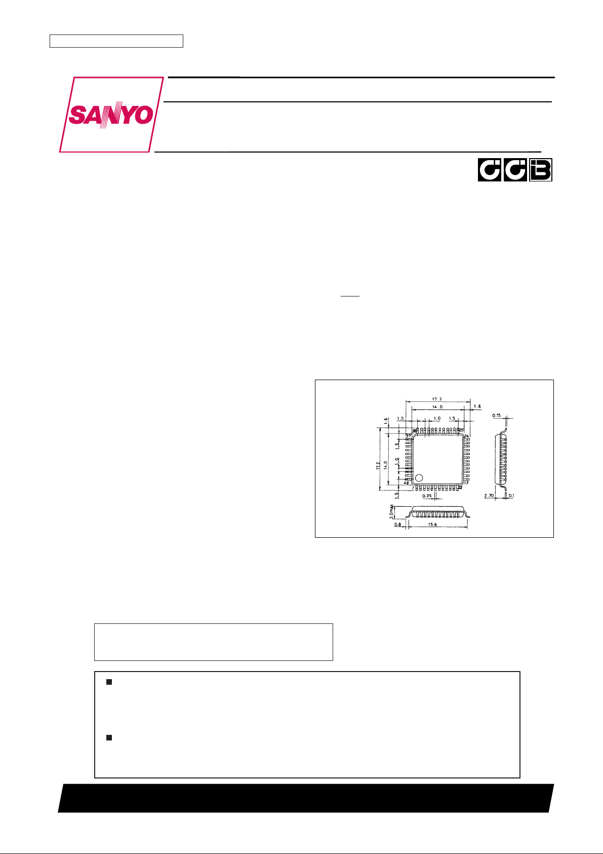
Package Dimensions
unit: mm
3156-QFP48E
• CCB is a trademark of SANYO ELECTRIC CO., LTD.
• CCB is a SANYO’s original bus format and all the
bus addresses are controlled by SANYO.
[LC75834E]
SANYO: QFP48E
Ordering number : EN5597A
93098HA (OT)/63097HA (OT) No. 5597-1/19
1/4 Duty General-Purpose
LCD Drivers
LC75834E, 75834W, 75834JE
SANYO Electric Co.,Ltd. Semiconductor Bussiness Headquarters
TOKYO OFFICE Tokyo Bldg., 1-10, 1 Chome, Ueno, Taito-ku, TOKYO, 110 JAPAN
CMOS LSI
Any and all SANYO products described or contained herein do not have specifications that can handle
applications that require extremely high levels of reliability, such as life-support systems, aircraft’s
control systems, or other applications whose failure can be reasonably expected to result in serious
physical and/or material damage. Consult with your SANYO representative nearest you before using
any SANYO products described or contained herein in such applications.
SANYO assumes no responsibility for equipment failures that result from using products at values that
exceed, even momentarily, rated values (such as maximum ratings, operating condition ranges, or other
parameters) listed in products specifications of any and all SANYO products described or contained
herein.
Continued to next page.
Page 2
Specifications
Absolute Maximum Ratings at Ta = 25°C, VSS= 0 V
Note: The LC75834JE do not have the S9, S18, S27 S34 output pins.
Allowable Operating Ranges at Ta = –40 to +85°C, VSS= 0 V
No. 5597-2/19
LC75834E, 75834W, 75834JE
Parameter Symbol Conditions Ratings Unit
Maximum supply voltage
V
DD
max V
DD
–0.3 to +7.0 V
V
LCD
max V
LCD
–0.3 to +7.0 V
V
IN
1 CE, CL, DI, INH –0.3 to +7.0 V
Input voltage V
IN
2 OSC –0.3 to VDD+ 0.3 V
V
IN
3 V
LCD
1, V
LCD
2 –0.3 to V
LCD
+ 0.3 V
Output voltage
V
OUT
1 OSC –0.3 to VDD+ 0.3 V
V
OUT
2 S1 to S34, COM1 to COM4, P1 to P8 –0.3 to V
LCD
+ 0.3 V
I
OUT
1 S1 to S34 300 µA
Output current I
OUT
2 COM1 to COM4 3 mA
I
OUT
3 P1 to P8 5 mA
Allowable power dissipation Pd max Ta = 85°C 150 mW
Operating temperature Topr –40 to +85 °C
Storage temperature Tstg –55 to +125 °C
Parameter Symbol Conditions
Ratings
Unit
min typ max
Supply voltage
V
DD
V
DD
2.7 6.0 V
V
LCD
V
LCD
2.7 6.0 V
Input voltage
V
LCD
1 V
LCD
1 2/3 V
LCD
V
LCD
V
V
LCD
2 V
LCD
2 1/3 V
LCD
V
LCD
V
Input high-level voltage V
IH
CE, CL, DI, INH 0.8 V
DD
6.0 V
Input low-level voltage V
IL
CE, CL, DI, INH 0 0.2 V
DD
V
Recommended external resistance R
OSC
OSC 43 kΩ
Recommended external capacitance C
OSC
OSC 680 pF
Guaranteed oscillation range f
OSC
OSC 25 50 100 kHz
Data setup time t
ds
CL, DI: Figure 2 160 ns
Data hold time t
dh
CL, DI: Figure 2 160 ns
CE wait time t
cp
CE, CL: Figure 2 160 ns
CE setup time t
cs
CE, CL: Figure 2 160 ns
CE hold time t
ch
CE, CL: Figure 2 160 ns
High-level clock pulse width t
øH
CL: Figure 2 160 ns
Low-level clock pulse width t
øL
CL: Figure 2 160 ns
Rise time t
r
CE, CL, DI: Figure 2 160 ns
Fall time t
f
CE, CL, DI: Figure 2 160 ns
INH switching time t
c
INH, CE: Figure 3 10 µs
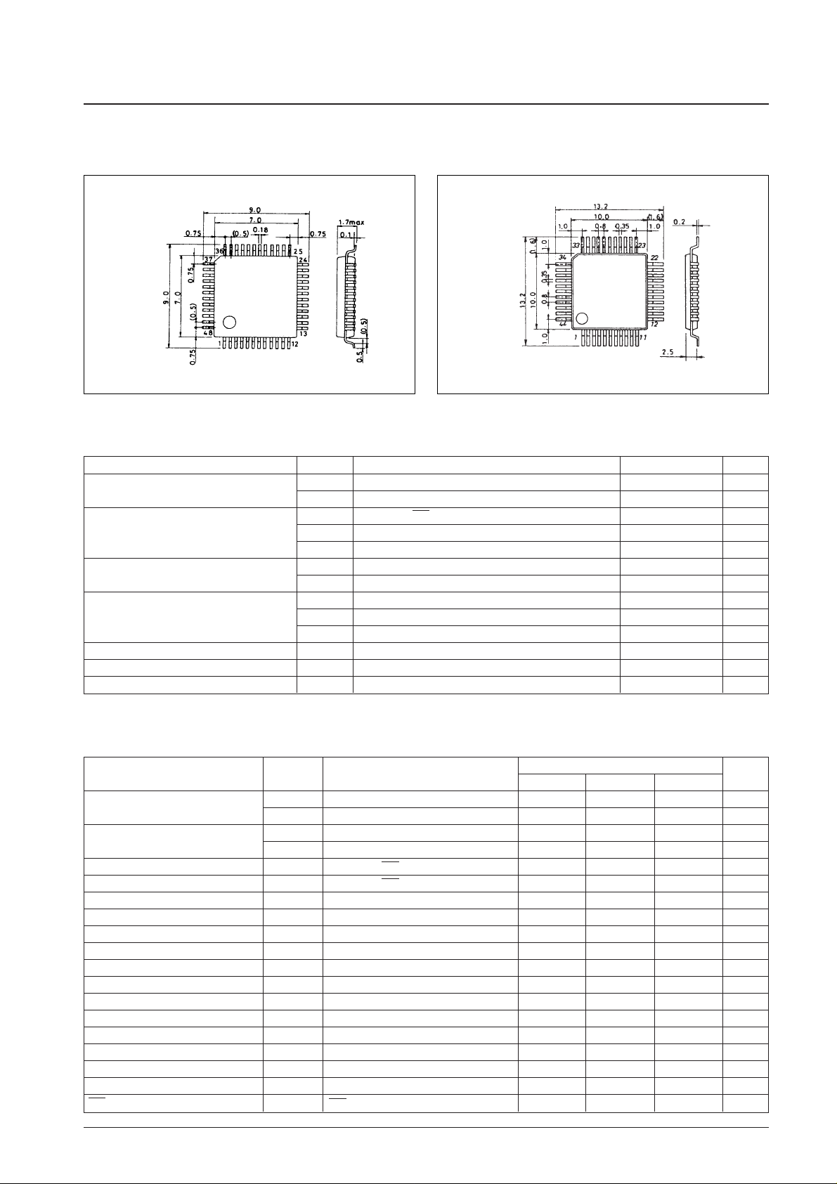
unit: mm
3163A-SQFP48
unit: mm
3148-QFP44MA
[LC75834JE]
SANYO: QIP44MA
[LC75834W]
SANYO: SQFP48
Continued from preceding page.
Page 3
No. 5597-3/19
LC75834E, 75834W, 75834JE
Electrical Characteristics for the Allowable Operating Ranges
Note: *1 Excluding the bias voltage generation divider resistors built in the V
LCD
1 and V
LCD
2. (See Figure 1.)
The LC75834JE do not have the S9, S18, S27, S34 output pins.
Parameter Symbol Conditions
Ratings
Unit
min typ max
Hysteresis width V
H
CE, CL, DI, INH 0.1 V
DD
V
Input high level current I
IH
CE, CL, DI, INH; VI= 6.0 V 5.0 µA
Input low level current I
IL
CE, CL, DI, INH; VI= 0 V –5.0 µA
V
OH
1 S1 to S34; IO= –20 µA V
LCD
– 0.9 V
Output high-level voltage V
OH
2 COM1 to COM4; IO= –100 µA V
LCD
– 0.9 V
V
OH
3 P1 to P8; IO= –1 mA V
LCD
– 0.9 V
V
OL
1 S1 to S34; IO= 20 µA 0.9 V
Output low-level voltage V
OL
2 COM1 to COM4; IO= 100 µA 0.9 V
V
OL
3 P1 to P8; IO= 1 mA 0.9 V
V
MID
1
COM1 to COM4; 1/2 bias,
1/2 V
LCD
– 0.9 1/2 V
LCD
+ 0.9 V
I
O
= ±100 µA
V
MID
2
S1 to S34; 1/3 bias,
2/3 V
LCD
– 0.9 2/3 V
LCD
+ 0.9 V
I
O
= ±20 µA
Output middle-level voltage*1
V
MID
3
S1 to S34; 1/3 bias,
1/3 V
LCD
– 0.9 1/3 V
LCD
+ 0.9 V
I
O
= ±20 µA
V
MID
4
COM1 to COM4; 1/3 bias,
2/3 V
LCD
– 0.9 2/3 V
LCD
+ 0.9 V
I
O
= ±100 µA
V
MID
5
COM1 to COM4; 1/3 bias,
1/3 V
LCD
– 0.9 1/3 V
LCD
+ 0.9 V
I
O
= ±100 µA
Oscillator frequency f
OSC
OSC; R
OSC
= 43 kΩ C
OSC
= 680 pF 40 50 60 kHz
I
DD
1 VDD; power saving mode 5 µA
I
DD
2 VDD; VDD= 6.0 V, output open, fosc = 50 k Hz 230 460 µA
I
LCD
1 V
LCD
; power saving mode 5 µA
Current drain
I
LCD
2
V
LCD
; V
LCD
= 6.0 V, output open
100 200 µA
1/2 bias, fosc = 50 k Hz
I
LCD
3
V
LCD
; V
LCD
= 6.0 V, output open
60 120 µA
1/3 bias, fosc = 50 k Hz
Page 4
Figure 1
1. When CL is stopped at the low level
2. When CL is stopped at the high level
Figure 2
No. 5597-4/19
LC75834E, 75834W, 75834JE
V
LCD
1
V
LCD
2
V
LCD
V
SS
A06588
To the common segments driver
Except these resistors
s
Page 5
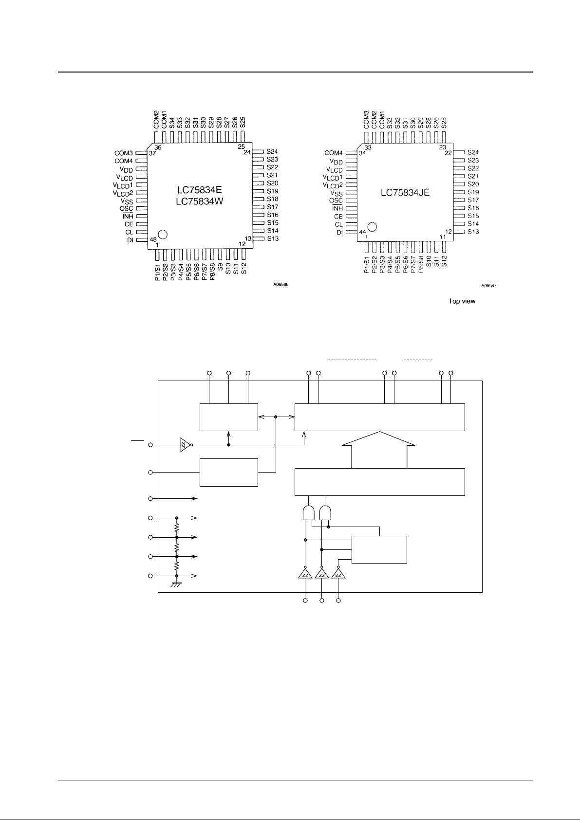
Pin Assignments
Block Diagram
Note: The LC75834JE do not have the S9, S18, S27, S34 output pins.
No. 5597-5/19
LC75834E, 75834W, 75834JE
Common
driver
Address
detector
Clock
generator
Segment driver & latch
Shift register
INH
OSC
V
DD
V
LCD
V
LCD
1
V
LCD
2
V
SS
DI
CL
CE
COM3
COM2
COM1
S35
S34
S9
S8/P8
S2/P2
S1/P1
A06591
Page 6
Pin Functions
Note: The LC75834JE do not have the S9, S18, S27, S34 output pins.
No. 5597-6/19
LC75834E, 75834W, 75834JE
CE: Chip enable
CL: Synchronization clock
DI: Transfer data
H
—
S1/P1 to
S8/P8
S9 to S34
Pin
1 to 8
9 to 34
LC75834E,
75834W
LC75834JE
1 to 8
9 to 30
— O Open
Segment outputs for displaying the display data transferred by serial data
input. The pins S1/P1 to S8/P8 can be used as general-purpose output ports
when so set up by the control data.
COM1
COM2
COM3
COM4
35
36
37
38
31
32
33
34
— O Open
Common driver outputs.
The frame frequency f
O
is given by: fO= (f
OSC
/512) Hz.
OSC
44 40
CE
CL
DI
46
47
48
42
43
44
Serial data transfer inputs. These
pins are connected to the control
microprocessor.
—
I/O
V
DD
I GND
Oscillator connection
An oscillator circuit is formed by connecting an external resistor and capacitor
V
LCD
1
41 37 — I Open
Used to apply the LCD drive 2/3-bias voltage externally. This pin must be
connected to V
LCD
2 when 1/2-bias drive is used.
V
LCD
2
42 38 — I Open
Used to apply the LCD drive 1/3-bias voltage externally. This pin must be
connected to V
LCD
1 when 1/2-bias drive is used.
V
DD
39 35 — — —Logic block power supply. Provide a voltage in the range 2.7 to 6.0 V.
V
LCD
40 36 — — —LCD driver block power supply. Provide a voltage in the range 2.7 to 6.0 V.
V
SS
43 39 — — —Ground pin. Connect to ground.
INH 45 41 L I GND
Display off control input
•INH = low (V
SS
): Off
S1/P1 to S8/P8 = Low
(These pins are forcible set to the segment output port
function and fixed at the V
SS
level.)
S9 to S34 = Low (V
SS
),
COM1 to COM4 = Low (V
SS
)
•INH = high (V
DD
): On
Note that serial data transfers can be performed when the
display is forced off by this pin.
Active I/O
Handling
when unused
Function
Pin No.
Page 7

Serial Data Transfer Format
1. When CL is stopped at the low level
Note: DD ... Direction data
No. 5597-7/19
LC75834E, 75834W, 75834JE
Page 8

2. When CL is stopped at the high level
Note: DD ... Direction data
• CCB address...............46H
• D1 to D136.................Display data (At the LC75834JE, the display data D33 to D36, D69 to D72, D105 to D108,
D133 to D136 must be set to 0.
• P0 to P3......................Segment output port/general-purpose output port switching control data
• DR..............................1/2-bias drive or 1/3-bias drive switching control data
• SC...............................Segments on/off control data
• BU..............................Normal mode/power-saving mode control data
No. 5597-8/19
LC75834E, 75834W, 75834JE
CCB address
8 bits
CCB address
8 bits
CCB address
8 bits
CCB address
8 bits
Display data
36 bits
Display data
36 bits
Display data
36 bits
Display data
28 bits
Control data
10 bits
Fixed data
10 bits
Fixed data
10 bits
Fixed data
18 bits
DD
2 bits
DD
2 bits
DD
2 bits
DD
2 bits
Page 9

Serial Data Transfer Examples
• At the LC75834E and LC75834W when109 or more segments are used, at the LC75834JE when 97 or more segments
are used,192 bits of serial data must be sent.
Note: At the LC75834JE, the display data D33 to D36, D69 to D72, D105 to D108, D133 to D136 must be set to 0.
• At the LC75834E and LC75834W when used with less than 109 segments, at the LC75834JE when used with less than
97 segments, transfer either 48 bits, 96 bits or 144 bits of serial data depending on the number of segments used.
However, the serial data shown in the figure below (the display data D1 to D36 and the control data) must be sent.
Note: At the LC75834JE, the display data D33 to D36 must be set to 0.
Control Data Functions
1. P0 to P3: Segment output port/general-purpose output port switching control data.
These control data bits switch the S1/P1 to S8/P8 output pins between their segment output port and general-purpose
output port functions.
Note: Sn (n = 1 to 8): Segment output ports
Pn (n = 1 to 8): General-purpose output ports
No. 5597-9/19
LC75834E, 75834W, 75834JE
Control data Output pin states
P0 P1 P2 P3 S1/P1 S2/P2 S3/P3 S4/P4 S5/P5 S6/P6 S7/P7 S8/P8
0 0 0 0 S1 S2 S3 S4 S5 S6 S7 S8
0 0 0 1 P1 S2 S3 S4 S5 S6 S7 S8
0 0 1 0 P1 P2 S3 S4 S5 S6 S7 S8
0 0 1 1 P1 P2 P3 S4 S5 S6 S7 S8
0 1 0 0 P1 P2 P3 P4 S5 S6 S7 S8
0 1 0 1 P1 P2 P3 P4 P5 S6 S7 S8
0 1 1 0 P1 P2 P3 P4 P5 P6 S7 S8
0 1 1 1 P1 P2 P3 P4 P5 P6 P7 S8
1 0 0 0 P1 P2 P3 P4 P5 P6 P7 P8
Page 10

Also note that when the general-purpose output port function is selected, the output pins and the display data will
have the correspondences listed in the tables below.
For example, if the output pin S4/P4 has the general-purpose output port function selected, it will output a high level
(V
LCD
) when the display data D13 is 1, and will output a low level (VSS) when D13 is 0.
2. DR: 1/2-bias drive or 1/3-bias drive switching control data
This control data bit selects either 1/2-bias drive or 1/3-bias drive.
3. SC: Segments on/off control data
This control data bit controls the on/off state of the segments.
However, note that when the segments are turned off by setting SC to 1, the segments are turned off by outputting
segment off waveforms from the segment output pins.
4. BU: Normal mode/power-saving mode control data
This control data bit selects either normal mode or power-saving mode.
No. 5597-10/19
LC75834E, 75834W, 75834JE
DR Drive type
0 1/3-bias drive
1 1/2-bias drive
SC Display state
0 On
1 Off
BU Mode
0 Normal mode
Power saving mode (The OSC pin oscillator is stopped, and the common and segment output pins go to the VSS level. However, the
1 S1/P1 to S8/P8 output pins that are set to be general-purpose output ports by the control data P0 to P3 can be used as general-
purpose output ports.)
Output pin Corresponding display data
S1/P1 D1
S2/P2 D5
S3/P3 D9
S4/P4 D13
Output pin Corresponding display data
S5/P5 D17
S6/P6 D21
S7/P7 D25
S8/P8 D29
Page 11

Display Data to Segment Output Pin Correspondence
Note: This applies to the case where the S1/P1 to S8/P8 output pins are set to be segment output ports.
The LC75834JE do not have the S9, S18, S27, S34 output pins.
For example, the table below lists the segment output states for the S11 output pin.
No. 5597-11/19
LC75834E, 75834W, 75834JE
Segment
COM1 COM2 COM3 COM4
output pin
S1/P1 D1 D2 D3 D4
S2/P2 D5 D6 D7 D8
S3/P3 D9 D10 D11 D12
S4/P4 D13 D14 D15 D16
S5/P5 D17 D18 D19 D20
S6/P6 D21 D22 D23 D24
S7/P7 D25 D26 D27 D28
S8/P8 D29 D30 D31 D32
S9 D33 D34 D35 D36
S10 D37 D38 D39 D40
S11 D41 D42 D43 D44
S12 D45 D46 D47 D48
S13 D49 D50 D51 D52
S14 D53 D54 D55 D56
S15 D57 D58 D59 D60
S16 D61 D62 D63 D64
S17 D65 D66 D67 D68
Segment
COM1 COM2 COM3 COM4
output pin
S18 D69 D70 D71 D72
S19 D73 D74 D75 D76
S20 D77 D78 D79 D80
S21 D81 D82 D83 D84
S22 D85 D86 D87 D88
S23 D89 D90 D91 D92
S24 D93 D94 D95 D96
S25 D97 D98 D99 D100
S26 D101 D102 D103 D104
S27 D105 D106 D107 D108
S28 D109 D110 D111 D112
S29 D113 D114 D115 D116
S30 D117 D118 D119 D120
S31 D121 D122 D123 D124
S32 D125 D126 D127 D128
S33 D129 D130 D131 D132
S34 D133 D134 D135 D136
Display data
Segment output pin (S11) state
D41 D42 D43 D44
0 0 0 0 The LCD segments corresponding to COM1 to COM4 are off.
0 0 0 1 The LCD segments corresponding to COM4 is on.
0 0 1 0 The LCD segments corresponding to COM3 is on.
0 0 1 1 The LCD segments corresponding to COM3 and COM4 are on.
0 1 0 0 The LCD segments corresponding to COM2 is on.
0 1 0 1 The LCD segments corresponding to COM2 and COM4 are on.
0 1 1 0 The LCD segments corresponding to COM2 and COM3 are on.
0 1 1 1 The LCD segments corresponding to COM2, COM3 and COM4 are on.
1 0 0 0 The LCD segments corresponding to COM1 is on.
1 0 0 1 The LCD segments corresponding to COM1 and COM4 are on.
1 0 1 0 The LCD segments corresponding to COM1 and COM3 are on.
1 0 1 1 The LCD segments corresponding to COM1, COM3 and COM4 are on.
1 1 0 0 The LCD segments corresponding to COM1 and COM2 are on.
1 1 0 1 The LCD segments corresponding to COM1, COM2 and COM4 are on.
1 1 1 0 The LCD segments corresponding to COM1 to COM3 are on.
1 1 1 1 The LCD segments corresponding to COM1 to COM4 are on.
Page 12

1/4 Duty, 1/2 Bias Drive Technique
No. 5597-12/19
LC75834E, 75834W, 75834JE
1/4 Duty, 1/2 Bias Waveforms
LCD driver output when all LCD
segments corresponding to COM1,
COM2, COM3, and COM4 are turned off.
LCD driver output when only LCD
segments corresponding to COM1 are
on.
LCD driver output when only LCD
segments corresponding to COM2 are
on.
LCD driver output when only LCD
segments corresponding to COM4 are
on.
LCD driver output when LCD segments
corresponding to COM1 and COM2 are
on.
LCD driver output when only LCD
segments corresponding to COM3 are
on.
LCD driver output when LCD segments
corresponding to COM1 and COM3 are
on.
LCD driver output when LCD segments
corresponding to COM2 and COM3 are
on.
LCD driver output when all LCD
segments corresponding to COM1,
COM2,COM3, and COM4 are on.
LCD driver output when LCD segments
corresponding to COM2 and COM4 are
on.
LCD driver output when LCD segments
corresponding to COM1, COM2, and
COM3 are on.
COM1
COM2
COM3
COM4
Page 13

No. 5597-13/19
LC75834E, 75834W, 75834JE
1/4 Duty, 1/3 Bias Drive Technique
1/4 Duty, 1/3 Bias Waveforms
LCD driver output when all LCD
segments corresponding to COM1,
COM2, COM3, and COM4 are turned off.
LCD driver output when only LCD
segments corresponding to COM1 are
on.
LCD driver output when only LCD
segments corresponding to COM2 are
on.
LCD driver output when only LCD
segments corresponding to COM4 are
on.
LCD driver output when LCD segments
corresponding to COM1 and COM2 are
on.
LCD driver output when only LCD
segments corresponding to COM3 are
on.
LCD driver output when LCD segments
corresponding to COM1 and COM3 are
on.
LCD driver output when LCD segments
corresponding to COM2 and COM3 are
on.
LCD driver output when all LCD
segments corresponding to COM1,
COM2,COM3, and COM4 are on.
LCD driver output when LCD segments
corresponding to COM2 and COM4 are
on.
LCD driver output when LCD segments
corresponding to COM1, COM2, and
COM3 are on.
COM1
COM2
COM3
COM4
Page 14

No. 5597-14/19
LC75834E, 75834W, 75834JE
The INH pin and Display Control
Since the LSI internal data (the display data and the control data) is undefined when power is first applied, applications
should set the INH pin low at the same time as power is applied to turn off the display (LC75834E, LC75834W: This
sets the S1/P1 to S8/P8, S9 to S34, and COM1 to COM4 to the VSSlevel. LC75834JE: This sets the S1/P1 to S8/P8, S10
to S17, S19 to S26, S28 to S33, and COM1 to COM4 to the VSSlevel.) and during this period send serial data from the
controller. The controller should then set the INH pin high after the data transfer has completed. This procedure prevents
meaningless displays at power on. (See Figure 3.)
Notes on the Power On/Off Sequences
Applications should observe the following sequence when turning the LC75834E, LC75834W, and LC75834JE power
on and off.
• At power on: Logic block power supply (VDD) on → LCD driver block power supply (V
LCD
) on
• At power off: LCD driver block power supply (V
LCD
) off → Logic block power supply (VDD) off
However, if the logic and LCD driver block use a shared power supply, then the power supplies can be turned on and off
at the same time.
Note: At the LC75834JE, the display data D33 to D36, D69 to D72, D105 to D108, D133 to D136 must be set to 0.
Figure 3
Notes on Controller Transfer of Display Data
Since the LC75834E, LC75834W, and LC75834JE accept display data divided into four separate transfer operations, we
recommend that applications transfer all of the display data within a period of less than 30 ms to prevent observable
degradation of display quality.
Page 15

Sample Application Circuit 1
1/2 Bias (for use with normal size panels)
• LC75834E, LC75834W
Note: *2 When a capacitor except the recommended external capacitance (C
OSC
= 680 pF) is connected the OSC pin, we recommend that applications
connect the OSC pin with a capacitor in the range 220 to 2200pF.
• LC75834JE
Note: *2 When a capacitor except the recommended external capacitance (C
OSC
= 680 pF) is connected the OSC pin, we recommend that applications
connect the OSC pin with a capacitor in the range 220 to 2200pF.
No. 5597-15/19
LC75834E, 75834W, 75834JE
From the
microcontroller
C ≥ 0.047 µF
From the
microcontroller
C ≥ 0.047 µF
Page 16

No. 5597-16/19
LC75834E, 75834W, 75834JE
Sample Application Circuit 2
1/2 Bias (for use with large panels)
• LC75834E, LC75834W
Note: *2 When a capacitor except the recommended external capacitance (C
OSC
= 680 pF) is connected the OSC pin, we recommend that applications
connect the OSC pin with a capacitor in the range 220 to 2200pF.
• LC75834JE
Note: *2 When a capacitor except the recommended external capacitance (C
OSC
= 680 pF) is connected the OSC pin, we recommend that applications
connect the OSC pin with a capacitor in the range 220 to 2200pF.
From the
microcontroller
10 kΩ ≥ R ≥ 1 kΩ
C ≥ 0.047 µF
10 kΩ ≥ R ≥ 1 kΩ
C ≥ 0.047 µF
From the
microcontroller
Page 17

Sample Application Circuit 3
1/3 Bias (for use with normal size panels)
• LC75834E, LC75834W
Note: *2 When a capacitor except the recommended external capacitance (C
OSC
= 680 pF) is connected the OSC pin, we recommend that applications
connect the OSC pin with a capacitor in the range 220 to 2200pF.
• LC75834JE
Note: *2 When a capacitor except the recommended external capacitance (C
OSC
= 680 pF) is connected the OSC pin, we recommend that applications
connect the OSC pin with a capacitor in the range 220 to 2200pF.
No. 5597-17/19
LC75834E, 75834W, 75834JE
C ≥ 0.047 µF
C ≥ 0.047 µF
From the
microcontroller
From the
microcontroller
Page 18

Sample Application Circuit 4
1/3 Bias (for use with large panels)
• LC75834E, LC75834W
Note: *2 When a capacitor except the recommended external capacitance (C
OSC
= 680 pF) is connected the OSC pin, we recommend that applications
connect the OSC pin with a capacitor in the range 220 to 2200pF.
Note: *2 When a capacitor except the recommended external capacitance (C
OSC
= 680 pF) is connected the OSC pin, we recommend that applications
connect the OSC pin with a capacitor in the range 220 to 2200pF.
No. 5597-18/19
LC75834E, 75834W, 75834JE
From the
microcontroller
10 kΩ ≥ R ≥ 1 kΩ
C ≥ 0.047 µF
10 kΩ ≥ R ≥ 1 kΩ
C ≥ 0.047 µF
From the
microcontroller
• LC75834JE
Page 19

PS No. 5597-19/19
LC75834E, 75834W, 75834JE
This catalog provides information as of September, 1998. Specifications and information herein are
subject to change without notice.
Specifications of any and all SANYO products described or contained herein stipulate the performance,
characteristics, and functions of the described products in the independent state, and are not guarantees
of the performance, characteristics, and functions of the described products as mounted in the customer’s
products or equipment. To verify symptoms and states that cannot be evaluated in an independent device,
the customer should always evaluate and test devices mounted in the customer’s products or equipment.
SANYO Electric Co., Ltd. strives to supply high-quality high-reliability products. However, any and all
semiconductor products fail with some probability. It is possible that these probabilistic failures could
give rise to accidents or events that could endanger human lives, that could give rise to smoke or fire,
or that could cause damage to other property. When designing equipment, adopt safety measures so
that these kinds of accidents or events cannot occur. Such measures include but are not limited to protective
circuits and error prevention circuits for safe design, redundant design, and structural design.
In the event that any or all SANYO products (including technical data, services) described or contained
herein are controlled under any of applicable local export control laws and regulations, such products must
not be exported without obtaining the export license from the authorities concerned in accordance with the
above law.
No part of this publication may be reproduced or transmitted in any form or by any means, electronic or
mechanical, including photocopying and recording, or any information storage or retrieval system,
or otherwise, without the prior written permission of SANYO Electric Co., Ltd.
Any and all information described or contained herein are subject to change without notice due to
product/technology improvement, etc. When designing equipment, refer to the “Delivery Specification”
for the SANYO product that you intend to use.
Information (including circuit diagrams and circuit parameters) herein is for example only; it is not
guaranteed for volume production. SANYO believes information herein is accurate and reliable, but
no guarantees are made or implied regarding its use or any infringements of intellectual property rights
or other rights of third parties.
 Loading...