

Page 1
CMOS LSI
Ordering number : EN 5580A
33098HA(OT)/22897HA(OT) No. 5580-1/19
SANYO Electric Co.,Ltd. Semiconductor Bussiness Headquarters
TOKYO OFFICE Tokyo Bldg., 1-10, 1 Chome, Ueno, Taito-ku, TOKYO, 110-8534 JAPAN
1/3 Duty General-Purpose
LCD Display Drivers
LC75833E, 75833W, 75833JE
Overview
The LC75833E, LC75833W, and LC75833JE are 1/3-duty
general-purpose LCD display drivers that can be used for
frequency display in electronic tuners under the control of
a microcontroller. The LC75833E and LC75833W can
drive an LCD with up to 105 segments directly, the
LC75833JE can drive an LCD with up to 93 segments
directly. The LC75833E and LC75833W and LC75833JE
can also control up to 8 general-purpose output ports.
Since the LC75833E, LC75833W, and LC75833JE use
separate power supply systems for the LCD drive block
and the logic block, the LCD driver block power-supply
voltage can be set to any voltage in the range 2.7 to 6.0
volts, regardless of the logic block power-supply voltage.
Features
• Supports both 1/3 duty 1/2 bias and 1/3 duty 1/3 bias
LCD drive under serial data control.
LC75833E, LC75833W: up to 105 segments
LC75833JE: up to 93 segments
(without the S12, S23, S24, S35 segment output pins
from the LC75833E, LC75833W)
• Serial data input supports CCB format communication
with the system controller.
• Serial data control of the power-saving mode based
backup function and all the segments forced off function
• Serial data control of switching between the segment
output port and the general-purpose output port
functions
• High generality, since display data is displayed directly
without decoder intervention.
• Independent V
LCD
for the LCD driver block (V
LCD
can
be set to any voltage in the range 2.7 to 6.0 volts,
regardless of the logic block power-supply voltage.)
• The INH pin can force the display to the off state.
• RC oscillator circuit
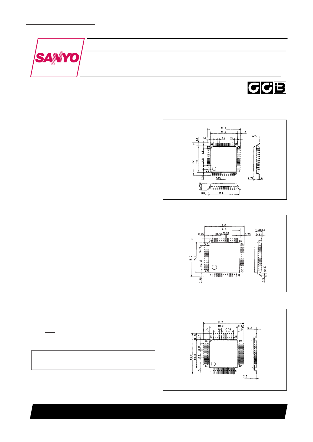
Package Dimensions
unit: mm
3156-QFP48E
unit: mm
3163A-SQFP48
unit: mm
3148-QFP44MA
• CCB is a trademark of SANYO ELECTRIC CO., LTD.
• CCB is SANYO’s original bus format and all the bus
addresses are controlled by SANYO.
[LC75833W]
[LC75833E]
SANYO: QFP48E
[LC75833JE]
SANYO: SQFP48
SANYO: QIP44MA
Page 2

Specifications
Absolute Maximum Ratings at Ta = 25°C, VSS= 0 V
Note: The LC75833JE does not have the S12, S23, S24, S35 output pins.
Allowable Operating Ranges at Ta = –40 to +85°C, VSS= 0 V
No. 5580-2/19
LC75833E, 75833W, 75833JE
Parameter Symbol Conditions Ratings Unit
Maximum supply voltage
V
DD
max V
DD
–0.3 to +7.0 V
V
LCD
max V
LCD
–0.3 to +7.0 V
V
IN
1 CE, CL, DI, INH –0.3 to +7.0 V
Input voltage V
IN
2 OSC –0.3 to VDD+ 0.3 V
V
IN
3 V
LCD
1, V
LCD
2 –0.3 to V
LCD
+ 0.3 V
Output voltage
V
OUT
1 OSC –0.3 to VDD+ 0.3 V
V
OUT
2 S1 to S35, COM1 to COM3, P1 to P8 –0.3 to V
LCD
+ 0.3 V
I
OUT
1 S1 to S35 300 µA
Output current I
OUT
2 COM1 to COM3 3 mA
I
OUT
3 P1 to P8 5 mA
Allowable power dissipation Pd max Ta = 85°C 150 mW
Operating temperature Topr –40 to +85 °C
Storage temperature Tstg –55 to +125 °C
Parameter Symbol Conditions
Ratings
Unit
min typ max
Supply voltage
V
DD
V
DD
2.7 6.0 V
V
LCD
V
LCD
2.7 6.0 V
Input voltage
V
LCD
1 V
LCD
1 2/3 V
LCD
V
LCD
V
V
LCD
2 V
LCD
2 1/3 V
LCD
V
LCD
V
Input high-level voltage V
IH
CE, CL, DI, INH 0.8 V
DD
6.0 V
Input low-level voltage V
IL
CE, CL, DI, INH 0 0.2 V
DD
V
Recommended external resistance R
OSC
OSC 39 kΩ
Recommended external capacitance C
OSC
OSC 1000 pF
Guaranteed oscillation range f
OSC
OSC 19 38 76 kHz
Data setup time t
ds
CL, DI: Figure 2 160 ns
Data hold time t
dh
CL, DI: Figure 2 160 ns
CE wait time t
cp
CE, CL: Figure 2 160 ns
CE setup time t
cs
CE, CL: Figure 2 160 ns
CE hold time t
ch
CE, CL: Figure 2 160 ns
High-level clock pulse width t
øH
CL: Figure 2 160 ns
Low-level clock pulse width t
øL
CL: Figure 2 160 ns
Rise time t
r
CE, CL, DI: Figure 2 160 ns
Fall time t
f
CE, CL, DI: Figure 2 160 ns
INH switching time t
c
INH, CE: Figure 3 10 µs
Page 3
No. 5580-3/19
LC75833E, 75833W, 75833JE
Electrical Characteristics for the Allowable Operating Ranges
Note: *1 Excluding the bias voltage generation divider resistors built in the V
LCD
1 and V
LCD
2. (See Figure 1.)
The LC75833JE does not have the S12, S23, S24, S35 output pins.
Parameter Symbol Conditions
Ratings
Unit
min typ max
Hysteresis width V
H
CE, CL, DI, INH 0.1 V
DD
V
Input high level current I
IH
CE, CL, DI, INH; VI= 6.0 V 5.0 µA
Input low level current I
IL
CE, CL, DI, INH; VI= 0 V –5.0 µA
V
OH
1 S1 to S35; IO= –20 µA V
LCD
– 0.9 V
Output high-level voltage V
OH
2 COM1 to COM3; IO= –100 µA V
LCD
– 0.9 V
V
OH
3 P1 to P8; IO= –1 mA V
LCD
– 0.9 V
V
OL
1 S1 to S35; IO= 20 µA 0.9 V
Output low-level voltage V
OL
2 COM1 to COM3; IO= 100 µA 0.9 V
V
OL
3 P1 to P8; IO= 1 mA 0.9 V
V
MID
1
COM1 to COM3; 1/2 bias,
1/2 V
LCD
– 0.9 1/2 V
LCD
+ 0.9 V
I
O
= ±100 µA
V
MID
2
S1 to S35; 1/3 bias,
2/3 V
LCD
– 0.9 2/3 V
LCD
+ 0.9 V
I
O
= ±20 µA
Output middle-level voltage*1
V
MID
3
S1 to S35; 1/3 bias,
1/3 V
LCD
– 0.9 1/3 V
LCD
+ 0.9 V
I
O
= ±20 µA
V
MID
4
COM1 to COM3; 1/3 bias,
2/3 V
LCD
– 0.9 2/3 V
LCD
+ 0.9 V
I
O
= ±100 µA
V
MID
5
COM1 to COM3; 1/3 bias,
1/3 V
LCD
– 0.9 1/3 V
LCD
+ 0.9 V
I
O
= ±100 µA
Oscillator frequency f
OSC
OSC; R
OSC
= 39 kΩ C
OSC
= 1000 pF 30.4 38 45.6 kHz
I
DD
1 VDD; power saving mode 5 µA
I
DD
2 VDD; VDD= 6.0 V, output open, fosc = 38 k Hz 250 500 µA
I
LCD
1 V
LCD
; power saving mode 5 µA
Current drain
I
LCD
2
V
LCD
; V
LCD
= 6.0 V, output open
100 200 µA
1/2 bias, fosc = 38 k Hz
I
LCD
3
V
LCD
; V
LCD
= 6.0 V, output open
60 120 µA
1/3 bias, fosc = 38 k Hz
Page 4

2. When CL is stopped at the high level
Figure 2
No. 5580-4/19
LC75833E, 75833W, 75833JE
V
LCD
1
V
LCD
2
V
LCD
V
SS
A06550
To the common segments driver
Except these resistors
s
tøH tøL
tr tf
tds tdh
tcp tcs
tch
V
IL
V
IH
V
IH
V
IH
V
IL
V
IL
50%
CL
CE
DI
A06551
V
IH
tøL tøH
tf tr
tds tdh
tcp tcs
tch
V
IL
V
IH
V
IH
V
IL
V
IL
50%
CL
CE
DI
A06552
Figure 1
1. When CL is stopped at the low level
Page 5

Pin Assignments
Block Diagram
Note: The LC75833JE does not have the S12, S23, S24, S35 output pins.
No. 5580-5/19
LC75833E, 75833W, 75833JE
COM2
37
COM3
V
DD
V
LCD
V
LCD
1
V
LCD
2
V
SS
OSC
INH
CE
CL
DI
48
S24
S23
S22
S21
S20
S19
S18
S17
S16
S15
S14
S13
13
24
P1/S1
1
12
P2/S2
P3/S3
P4/S4
P5/S5
P6/S6
P7/S7
P8/S8
S9
S10
S11
S12 S25
2536
S26
S27
S28
S29
S30
S31
S32
S33
S34
S35
COM1
LC75833E
LC75833W
A06549
34
COM3
V
DD
V
LCD
V
LCD
1
V
LCD
2
V
SS
OSC
INH
CE
CL
DI
44
S25
S22
S21
S20
S19
S18
S17
S16
S15
S14
S13
12
22
P1/S1
1
11
P2/S2
P3/S3
P4/S4
P5/S5
P6/S6
P7/S7
P8/S8
S9
S10
S11
2333
S26
S27
S28
S29
S30
S31
S32
S33
S34
COM1
COM2
LC75833JE
A06582
Common
driver
Address
detector
Clock
generator
Segment driver & latch
Shift register
INH
OSC
V
DD
V
LCD
V
LCD
1
V
LCD
2
V
SS
DI
CL
CE
COM3
COM2
COM1
S35
S34
S9
S8/P8
S2/P2
S1/P1
A06553
Page 6

Pin Functions
Note: The LC75833JE does not have the S12, S23, S24, S35 output pins.
No. 5580-6/19
LC75833E, 75833W, 75833JE
CE: Chip enable
CL: Synchronization clock
DI: Transfer data
H
—
S1/P1 to
S8/P8
S9 to S35
Pin
1 to 8
9 to 35
LC75833E,
75833W
LC75833JE
1 to 8
9 to 31
— O Open
Segment outputs for displaying the display data transferred by serial data
input. The pins S1/P1 to S8/P8 can be used as general-purpose output ports
when so set up by the control data.
COM1
COM2
COM3
36
37
38
32
33
34
— O Open
Common driver outputs.
The frame frequency f
O
is given by: fO= (f
OSC
/384) Hz.
OSC 44 40
CE
CL
DI
46
47
48
42
43
44
Serial data transfer inputs. These
pins are connected to the control
microprocessor.
— I/O
V
DD
I GND
Oscillator connection
An oscillator circuit is formed by connecting an external resistor and capacitor
to this pin.
V
LCD
1
41 37 — I Open
Used to apply the LCD drive 2/3-bias voltage externally. This pin must be
connected to V
LCD
2 when 1/2-bias drive is used.
V
LCD
2
42 38 — I Open
Used to apply the LCD drive 1/3-bias voltage externally. This pin must be
connected to V
LCD
1 when 1/2-bias drive is used.
V
DD
39 35 — — —Logic block power supply. Provide a voltage in the range 2.7 to 6.0 V.
V
LCD
40 36 — — —LCD driver block power supply. Provide a voltage in the range 2.7 to 6.0 V.
V
SS
43 39 — — —Ground pin. Connect to ground.
INH 45 41 L I GND
Display off control input
•INH = low (V
SS
): Off
S1/P1 to S8/P8 = Low
(These pins are forcibly set to the segment output port
function and fixed at the V
SS
level.)
S9 to S35 = Low (V
SS
),
COM1 to COM3 = Low (V
SS
)
•INH = high (V
DD
): On
Note that serial data transfers can be performed when the
display is forced off by this pin.
Active I/O
Handling
when unused
Functions
Pin No.
Page 7

Serial Data Transfer Format
1. When CL is stopped at the low level
Note: DD ... Direction data
No. 5580-7/19
LC75833E, 75833W, 75833JE
D32D3D2D101000110
A3A2A1A0B3B2B1B0
D33 D34 D35 D36 0 0 0 P0 P1 P2 P3 DR SC BU 0 0
CCB address
8 bits
Display data
36 bits
Control data
10 bits
DD
2 bits
CE
CL
DI
D68D39D38D3701000110
A3A2A1A0B3B2B1B0
D69 D70 D71 D72 0 0 0 0 0 0 0 0 0 0 0 1
CCB address
8 bits
Display data
36 bits
Fixed data
10 bits
DD
2 bits
D104
D75D74D7301000110
A3A2A1A0B3B2B1B0
D105
0 0 0 0 0 0 0 0 0 0 0 0 0 1 0
CCB address
8 bits
Display data
33 bits
Fixed data
13 bits
DD
2 bits
A06554
Page 8

2. When CL is stopped at the high level
Note: DD ... Direction data
• CCB address...............46H
• D1 to D105.................Display data (At the LC75833JE, the display data D34 to D36, D67 to D72, D103 to D105
must be set to 0.
• P0 to P3......................Segment output port/general-purpose output port switching control data
• DR..............................1/2-bias drive or 1/3-bias drive switching control data
• SC...............................Segments on/off control data
• BU..............................Normal mode/power-saving mode control data
No. 5580-8/19
LC75833E, 75833W, 75833JE
D32D3D2D101000110
A3A2A1A0B3B2B1B0
D33 D34 D35 D36 0 0 0 P0 P1 P2 P3 DR SC BU 0 0
CCB address
8 bits
Display data
36 bits
Control data
10 bits
DD
2 bits
CE
CL
DI
D68D39D38D3701000110
A3A2A1A0B3B2B1B0
D69 D70 D71 D72 0 0 0 0 0 0 0 0 0 0 0 1
CCB address
8 bits
Display data
36 bits
Fixed data
10 bits
DD
2 bits
D104
D75D74D7301000110
A3A2A1A0B3B2B1B0
D105
0 0 0 0 0 0 0 0 0 0 0 0 0 1 0
CCB address
8 bits
Display data
33 bits
Fixed data
13 bits
DD
2 bits
A06555
Page 9

Serial Data Transfer Examples
• At the LC75833E and LC75833W when 73 or more segments are used, at the LC75833JE when 64 or more segments
are used.
144 bits of serial data must be sent.
Note: At the LC75833JE, the display data D34 to D36, D67 to D72, D103 to D105 must be set to 0.
• At the LC75833E and LC75833W when used with less than 73 segments, at the LC75833JE when used with less than
64 segments.
Transfer either 48 bits or 96 bits of serial data depending on the number of segments used. However, the serial data
shown in the figure below (the display data D1 to D36 and the control data) must be sent.
Note: At the LC75833JE, the display data D34 to D36 must be set to 0.
Control Data Functions
1. P0 to P3: Segment output port/general-purpose output port switching control data.
These control data bits switch the S1/P1 to S8/P8 output pins between their segment output port and general-purpose
output port functions.
Note: Sn (n = 1 to 8): Segment output ports
Pn (n = 1 to 8): General-purpose output ports
No. 5580-9/19
LC75833E, 75833W, 75833JE
Control data Output pin states
P0 P1 P2 P3 S1/P1 S2/P2 S3/P3 S4/P4 S5/P5 S6/P6 S7/P7 S8/P8
0 0 0 0 S1 S2 S3 S4 S5 S6 S7 S8
0 0 0 1 P1 S2 S3 S4 S5 S6 S7 S8
0 0 1 0 P1 P2 S3 S4 S5 S6 S7 S8
0 0 1 1 P1 P2 P3 S4 S5 S6 S7 S8
0 1 0 0 P1 P2 P3 P4 S5 S6 S7 S8
0 1 0 1 P1 P2 P3 P4 P5 S6 S7 S8
0 1 1 0 P1 P2 P3 P4 P5 P6 S7 S8
0 1 1 1 P1 P2 P3 P4 P5 P6 P7 S8
1 0 0 0 P1 P2 P3 P4 P5 P6 P7 P8
8 bits 48 bits
D1 D2 D3 D31 D32 D330 1 1 0 0 0 1 0
B0 B1 B2 B3 A0 A1 A2 A3
D38 D39 D67 D68 D690 1 1 0 0 0 1 0
D37
B0 B1 B2 B3 A0 A1 A2 A3
0 1 1 0 0 0 1 0
B0 B1 B2 B3 A0 A1 A2 A3
D73 D74 D75
D103 D104 D105
D34 D35 D36 0 0 0 P0 P1 P2 P3 DR SC BU 0 0
D70 D71 D72 0 0 0 0 0 0 0 0 0 0 0 1
0 0 0 0 0 0 0 0 0 0 0 0 0 1 0
A06556
B0 B1 B2 B3 A0 A1 A2 A3
8 bits 48 bits
D1 D2 D3 D31 D32 D330 1 1 0 0 0 1 0
D34 D35 D36 0 0 0 P0 P1 P2 P3 DR SC BU 0 0
A06557
Page 10

Also note that when the general-purpose output port function is selected, the output pins and the display data will
have the correspondences listed in the tables below.
For example, if the output pin S4/P4 has the general-purpose output port function selected, it will output a high level
(V
LCD
) when the display data D10 is 1, and will output a low level (VSS) when D10 is 0.
2. DR: 1/2-bias drive or 1/3-bias drive switching control data
This control data bit selects either 1/2-bias drive or 1/3-bias drive.
3. SC: Segments on/off control data
This control data bit controls the on/off state of the segments.
However, note that when the segments are turned off by setting SC to 1, the segments are turned off by outputting
segment off waveforms from the segment output pins.
4. BU: Normal mode/power-saving mode control data
This control data bit selects either normal mode or power-saving mode.
No. 5580-10/19
LC75833E, 75833W, 75833JE
DR Drive type
0 1/3-bias drive
1 1/2-bias drive
SC Display state
0 On
1 Off
BU Mode
0 Normal mode
Power saving mode (The OSC pin oscillator is stopped, and the common and segment output pins go to the VSS level. However, the
1 S1/P1 to S8/P8 output pins that are set to be general-purpose output ports by the control data P0 to P3 can be used as general-
purpose output ports.)
Output pin Corresponding display data
S1/P1 D1
S2/P2 D4
S3/P3 D7
S4/P4 D10
Output pin Corresponding display data
S5/P5 D13
S6/P6 D16
S7/P7 D19
S8/P8 D22
Page 11

Display Data to Segment Output Pin Correspondence
Note: This applies to the case where the S1/P1 to S8/P8 output pins are set to be segment output ports.
The LC75833JE do not have the S12, S23, S24, S35 output pins.
For example, the table below lists the segment output states for the S11 output pin.
No. 5580-11/19
LC75833E, 75833W, 75833JE
Segment
COM1 COM2 COM3
output pin
S1/P1 D1 D2 D3
S2/P2 D4 D5 D6
S3/P3 D7 D8 D9
S4/P4 D10 D11 D12
S5/P5 D13 D14 D15
S6/P6 D16 D17 D18
S7/P7 D19 D20 D21
S8/P8 D22 D23 D24
S9 D25 D26 D27
S10 D28 D29 D30
S11 D31 D32 D33
S12 D34 D35 D36
S13 D37 D38 D39
S14 D40 D41 D42
S15 D43 D44 D45
S16 D46 D47 D48
S17 D49 D50 D51
S18 D52 D53 D54
Segment
COM1 COM2 COM3
output pin
S19 D55 D56 D57
S20 D58 D59 D60
S21 D61 D62 D63
S22 D64 D65 D66
S23 D67 D68 D69
S24 D70 D71 D72
S25 D73 D74 D75
S26 D76 D77 D78
S27 D79 D80 D81
S28 D82 D83 D84
S29 D85 D86 D87
S30 D88 D89 D90
S31 D91 D92 D93
S32 D94 D95 D96
S33 D97 D98 D99
S34 D100 D101 D102
S35 D103 D104 D105
Display data
Segment output pin (S11) state
D31 D32 D33
0 0 0 The LCD segments corresponding to COM1 to COM3 are off.
0 0 1 The LCD segments corresponding to COM3 is on.
0 1 0 The LCD segments corresponding to COM2 is on.
0 1 1 The LCD segments corresponding to COM2 and COM3 are on.
1 0 0 The LCD segments corresponding to COM1 is on.
1 0 1 The LCD segments corresponding to COM1 and COM3 are on.
1 1 0 The LCD segments corresponding to COM1 and COM2 are on.
1 1 1 The LCD segments corresponding to COM1 to COM3 are on.
Page 12

1/3-Duty 1/2-Bias Drive Technique
No. 5580-12/19
LC75833E, 75833W, 75833JE
1/3-Duty 1/2-Bias Waveforms
fosc
384
[Hz]
COM1
V
LCD
V
LCD1
, V
LCD2
0 V
V
LCD
V
LCD1
, V
LCD2
0 V
V
LCD
V
LCD1
, V
LCD2
0 V
V
LCD
V
LCD1
, V
LCD2
0 V
V
LCD
V
LCD1
, V
LCD2
0 V
V
LCD
V
LCD1
, V
LCD2
0 V
V
LCD
V
LCD1
, V
LCD2
0 V
V
LCD
V
LCD1
, V
LCD2
0 V
V
LCD
V
LCD1
, V
LCD2
0 V
V
LCD
V
LCD1
, V
LCD2
0 V
V
LCD
V
LCD1
, V
LCD2
0 V
COM2
COM3
A06558
LCD driver output when all LCD
segments corresponding to COM1,
COM2, and COM3 are turned off.
LCD driver output when only LCD
segments corresponding to
COM1 are on (lit).
LCD driver output when only LCD
segments corresponding to
COM2 are on.
LCD driver output when LCD
segments corresponding to
COM1 and COM2 are on.
LCD driver output when only LCD
segments corresponding to
COM3 are on.
LCD driver output when LCD
segments corresponding to
COM1 and COM3 are on.
LCD driver output when LCD
segments corresponding to
COM2 and COM3 are on.
LCD driver output when all LCD
segments corresponding to COM1,
COM2, and COM3 are on.
Page 13

fosc
384
[Hz]
COM1
V
LCD
V
LCD1
V
LCD2
0 V
V
LCD
V
LCD1
V
LCD2
0 V
V
LCD
V
LCD1
V
LCD2
0 V
V
LCD
V
LCD1
V
LCD2
0 V
V
LCD
V
LCD1
V
LCD2
0 V
V
LCD
V
LCD1
V
LCD2
0 V
V
LCD
V
LCD1
V
LCD2
0 V
V
LCD
V
LCD1
V
LCD2
0 V
V
LCD
V
LCD1
V
LCD2
0 V
V
LCD
V
LCD1
V
LCD2
0 V
V
LCD
V
LCD1
V
LCD2
0 V
COM2
COM3
1/3-Duty 1/3-Bias Technique
No. 5580-13/19
LC75833E, 75833W, 75833JE
LCD driver output when all LCD
segments corresponding to COM1,
COM2, and COM3 are turned off.
LCD driver output when only LCD
segments corresponding to
COM1 are on (lit).
LCD driver output when only LCD
segments corresponding to
COM2 are on.
LCD driver output when LCD
segments corresponding to
COM1 and COM2 are on.
LCD driver output when only LCD
segments corresponding to
COM3 are on.
LCD driver output when LCD
segments corresponding to
COM1 and COM3 are on.
LCD driver output when LCD
segments corresponding to
COM2 and COM3 are on.
LCD driver output when all LCD
segments corresponding to COM1,
COM2, and COM3 are on.
1/3-Duty 1/3-Bias Waveforms
A06559
Page 14

The INH pin and Display Control
Since the LSI internal data (the display data and the control data) is undefined when power is first applied, applications
should set the INH pin low at the same time as power is applied to turn off the display (LC75833E, LC75833W: This
sets the S1/P1 to S8/P8, S9 to S35, and COM1 to COM3 to the V
SS
level. LC75833JE: This sets the S1/P1 to S8/P8, S9
to S11, S13 to S22, S25 to S34, and COM1 to COM3 to the V
SS
level.) and during this period send serial data from the
controller. The controller should then set the INH pin high after the data transfer has completed. This procedure prevents
meaningless displays at power on. (See Figure 3.)
Notes on the Power On/Off Sequences
Applications should observe the following sequence when turning the LC75833E, LC75833W, and LC75833JE power
on and off.
• At power on: Logic block power supply (VDD) on → LCD driver block power supply (V
LCD
) on
• At power off: LCD driver block power supply (V
LCD
) off → Logic block power supply (VDD) off
However, if the logic and LCD driver block use a shared power supply, then the power supplies can be turned on and off
at the same time.
Figure 3
Notes on Controller Transfer of Display Data
Since the LC75833E, LC75833W, and LC75833JE accept display data divided into three separate transfer operations,
we recommend that applications transfer all of the display data within a period of less than 30 ms to prevent observable
degradation of display quality.
No. 5580-14/19
LC75833E, 75833W, 75833JE
V
DD
V
LCD
INH
CE
D1 to D36
P0 to P3
Internal data
Internal data
Internal data
DR, SC, BU
(D37 to D72)
(D73 to D105)
t 1
t 2
t 3
V
IL
tc
V
IL
Display and control data transfer
Undefined
Undefined
Undefined
Defined
Defined
Defined
Undefined
Undefined
Undefined
A06560
Note: At the LC75833JE, the display data D34 to D36, D67 to D72, D103 to D105 must be set to 0.
Note:
t1 ≥ 0
t2 > 0
t3 ≥ 0 (t2 > t3)
tc ... 10 µs min
Page 15

Sample Application Circuit 1
1/2 Bias (for use with normal size panels)
• LC75833E, LC75833W
Note: *2 When a capacitor except the recommended external capacitance (C
OSC
= 1000 pF) is connected the OSC pin, we recommend that applications
connect the OSC pin with a capacitor in the range 220 to 2200pF.
• LC75833JE
Note: *2 When a capacitor except the recommended external capacitance (C
OSC
= 1000 pF) is connected the OSC pin, we recommend that applications
connect the OSC pin with a capacitor in the range 220 to 2200pF.
No. 5580-15/19
LC75833E, 75833W, 75833JE
V
DD
V
SS
V
LCD
V
LCD1
V
LCD2
INH
CE
CL
DI
COM1
COM2
COM3
P1/S1
P2/S2
P8/S8
S9
S33
S34
S35
+3 V
+5 V
C ≥ 0.047 µF
From the
controller
OSC
*2
(P1)
(P2)
(P8)
General-purpose
output ports
Used for functions
such as backlight
control
A06561
LCD panel (up to 105 segments)
C
V
DD
V
SS
V
LCD
V
LCD1
V
LCD2
INH
CE
CL
DI
COM1
COM2
COM3
P1/S1
P2/S2
P8/S8
S9
S10
S11
S13
S22
S25
S34
+3 V
+5 V
From the
controller
OSC
*2
(P1)
(P2)
(P8)
General-purpose
output ports
Used for functions
such as backlight
control
LCD panel (up to 93 segments)
A06583
C ≥ 0.047 µF
C
Page 16

Sample Application Circuit 2
1/2 Bias (for use with large panels)
• LC75833E, LC75833W
Note: *2 When a capacitor except the recommended external capacitance (C
OSC
= 1000 pF) is connected the OSC pin, we recommend that applications
connect the OSC pin with a capacitor in the range 220 to 2200pF.
• LC75833JE
Note: *2 When a capacitor except the recommended external capacitance (C
OSC
= 1000 pF) is connected the OSC pin, we recommend that applications
connect the OSC pin with a capacitor in the range 220 to 2200pF.
No. 5580-16/19
LC75833E, 75833W, 75833JE
V
DD
V
SS
V
LCD
V
LCD1
V
LCD2
INH
CE
CL
DI
COM1
COM2
COM3
P1/S1
P2/S2
P8/S8
S9
S33
S34
S35
+3 V
+5 V
From the
controller
OSC
*2
(P1)
(P2)
(P8)
General-purpose
output ports
Used for functions
such as backlight
control
A06562
LCD panel (up to 105 segments)
C ≥ 0.047 µF
10kΩ ≥ R ≥ 1kΩ
C R
R
V
DD
V
SS
V
LCD
V
LCD1
V
LCD2
INH
CE
CL
DI
COM1
COM2
COM3
P1/S1
P2/S2
P8/S8
S9
S10
S11
S13
S22
S25
S34
OSC
*2
(P1)
(P2)
(P8)
General-purpose
output ports
Used for functions
such as backlight
control
A06584
+3 V
+5 V
From the
controller
LCD panel (up to 93 segments)
C ≥ 0.047 µF
10kΩ ≥ R ≥ 1kΩ
C R
R
Page 17

Sample Application Circuit 3
1/3 Bias (for use with normal size panels)
• LC75833E, LC75833W
Note: *2 When a capacitor except the recommended external capacitance (C
OSC
= 1000 pF) is connected the OSC pin, we recommend that applications
connect the OSC pin with a capacitor in the range 220 to 2200pF.
• LC75833JE
Note: *2 When a capacitor except the recommended external capacitance (C
OSC
= 1000 pF) is connected the OSC pin, we recommend that applications
connect the OSC pin with a capacitor in the range 220 to 2200pF.
No. 4801-17/19
LC75833E, 75833W, 75833JE
V
DD
V
SS
V
LCD
V
LCD1
V
LCD2
INH
CE
CL
DI
COM1
COM2
COM3
P1/S1
P2/S2
P8/S8
S9
S33
S34
S35
+3 V
+5 V
C ≥ 0.047 µF
From the
controller
OSC
*2
(P1)
(P2)
(P8)
General-purpose
output ports
Used for functions
such as backlight
control
A06562
CC
LCD panel (up to 105 segments)
V
DD
V
SS
V
LCD
V
LCD1
V
LCD2
INH
CE
CL
DI
COM1
COM2
COM3
P1/S1
P2/S2
P8/S8
S9
S10
S11
S13
S22
S25
S34
OSC
*2
(P1)
(P2)
(P8)
General-purpose
output ports
Used for functions
such as backlight
control
A06584
+3 V
+5 V
C ≥ 0.047 µF
From the
controller
CC
LCD panel (up to 93 segments)
Page 18

Sample Application Circuit 4
1/3 Bias (for use with large panels)
• LC75833E, LC75833W
Note: *2 When a capacitor except the recommended external capacitance (C
OSC
= 1000 pF) is connected the OSC pin, we recommend that applications
connect the OSC pin with a capacitor in the range 220 to 2200pF.
No. 5580-18/19
LC75833E, 75833W, 75833JE
V
DD
V
SS
V
LCD
V
LCD1
V
LCD2
INH
CE
CL
DI
COM1
COM2
COM3
P1/S1
P2/S2
P8/S8
S9
S33
S34
S35
OSC
*2
(P1)
(P2)
(P8)
General-purpose
output ports
Used for functions
such as backlight
control
A06563
LCD panel (up to 105 segments)
+3 V
+5 V
From the
controller
C ≥ 0.047 µF
10 kΩ ≥ R ≥ 1 kΩ
C C
R
R
R
Page 19

PS No. 5580-19/19
LC75833E, 75833W, 75833JE
• LC75833JE
Note: *2 When a capacitor except the recommended external capacitance (C
OSC
= 1000 pF) is connected the OSC pin, we recommend that applications
connect the OSC pin with a capacitor in the range 220 to 2200pF.
This catalog provides information as of March 1998. Specifications and information herein are subject to
change without notice.
■ No products described or contained herein are intended for use in surgical implants, life-support systems, aerospace
equipment, nuclear power control systems, vehicles, disaster/crime-prevention equipment and the like, the failure of
which may directly or indirectly cause injury, death or property loss.
■ Anyone purchasing any products described or contained herein for an above-mentioned use shall:
① Accept full responsibility and indemnify and defend SANYO ELECTRIC CO., LTD., its affiliates, subsidiaries and
distributors and all their officers and employees, jointly and severally, against any and all claims and litigation and all
damages, cost and expenses associated with such use:
➁ Not impose any responsibility for any fault or negligence which may be cited in any such claim or litigation on
SANYO ELECTRIC CO., LTD., its affiliates, subsidiaries and distributors or any of their officers and employees
jointly or severally.
■ Information (including circuit diagrams and circuit parameters) herein is for example only; it is not guaranteed for
volume production. SANYO believes information herein is accurate and reliable, but no guarantees are made or implied
regarding its use or any infringements of intellectual property rights or other rights of third parties.
C ≥ 0.047 µF
10 kΩ ≥ R ≥ 1 kΩ
From the
controller
+3 V
+5 V
C C
General-purpose
(P1)
output ports
(P2)
Used for functions
*2
such as backlight
(P8)
control
V
DD
OSC
COM1
COM2
V
SS
COM3
P1/S1
P2/S2
V
V
V
LCD
LCD1
LCD2
P8/S8
S9
S10
S11
R
R
R
S13
INH
CE
CL
S22
S25
LCD panel (up to 93 segments)
DI
S34
A06585
 Loading...