

Page 1
Ordering number: EN 4037C
Monolithic Linear IC
LA7577N
Super-split PLL- II VIF and SIF
IF Signal Processor for TV/VTRs
Overview
The LA7577N is a high tone quality and high picture quality, video IF and sound IF IC. It employs split processing
of the video IF signal and sound IF signal using SAW filters and a PLL detector. Further, the PLL detector incorporates a buzz canceler for Nyquist buzz interference
suppression to achieve high tone quality.
Functions
VIF stage
• VIF amplifier
• PLL detector
• B/W noise canceler
• RF AGC
• VCO
• Equalizer amplifier
• AFT
• APC detector
• APC filter
• Lock detector
• IF AGC
• Buzz canceler
Features
• Employs split processing for wide bandwidth video
characteristics
• PLL detector with buzz canceler for excellent buzz and
buzz beat characteristics
• APC time constant switch built-in
• High-speed AGC supports double time constant method
• SIF carrier level AGC in the 1st SIF stage for good SIF
weak electric field characteristics
• Good differential gain and phase characteristics
• RF AGC easily adjusted using a variable resistor
Package Dimensions
unit: mm
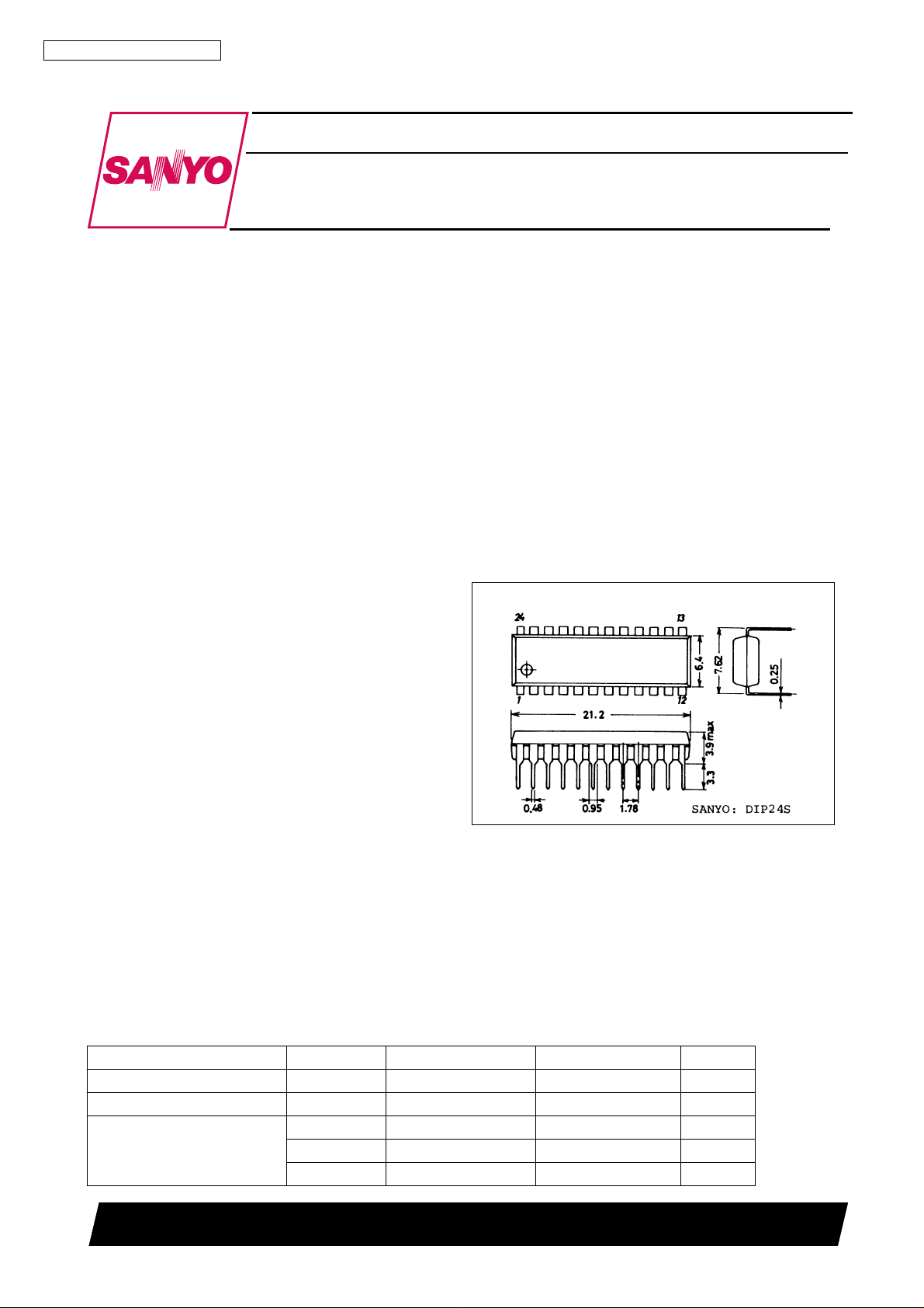
3067-DIP24S
[LA7577N]
1st SIF stage
• Preamplifier with AGC
• 1st SIF detector
SIF stage
• SIF limiter amplifier
• FM quadrature detector
Mute stage
• Sound mute (pin 2)
• AV mute (pin 4)
• IS-15 switch (pin 13)
Specifications
Absolute Maximum Ratings
Parameter Symbol Conditions Ratings Unit
Maximum supply voltage
Allowable power dissipation Pd max
Circuit voltages
at Ta = 25 ° C
V
max 13.8 V
CC
V
, V
3
V
11
V
23
Ta ≤ 50 ° C 1200 mW
13
V
CC
V
CC
V
CC
V
V
V
SANYO Electric Co., Ltd. Semiconductor Business Headquarters
TOKYO OFFICE Tokyo Bldg., 1-10, 1 Chome, Ueno, Taito-ku, TOKYO, 110 JAPAN
60597HA(ID) / 11795TH(ID) No. 4037—1/16
Page 2
−
−
−
−
−
−
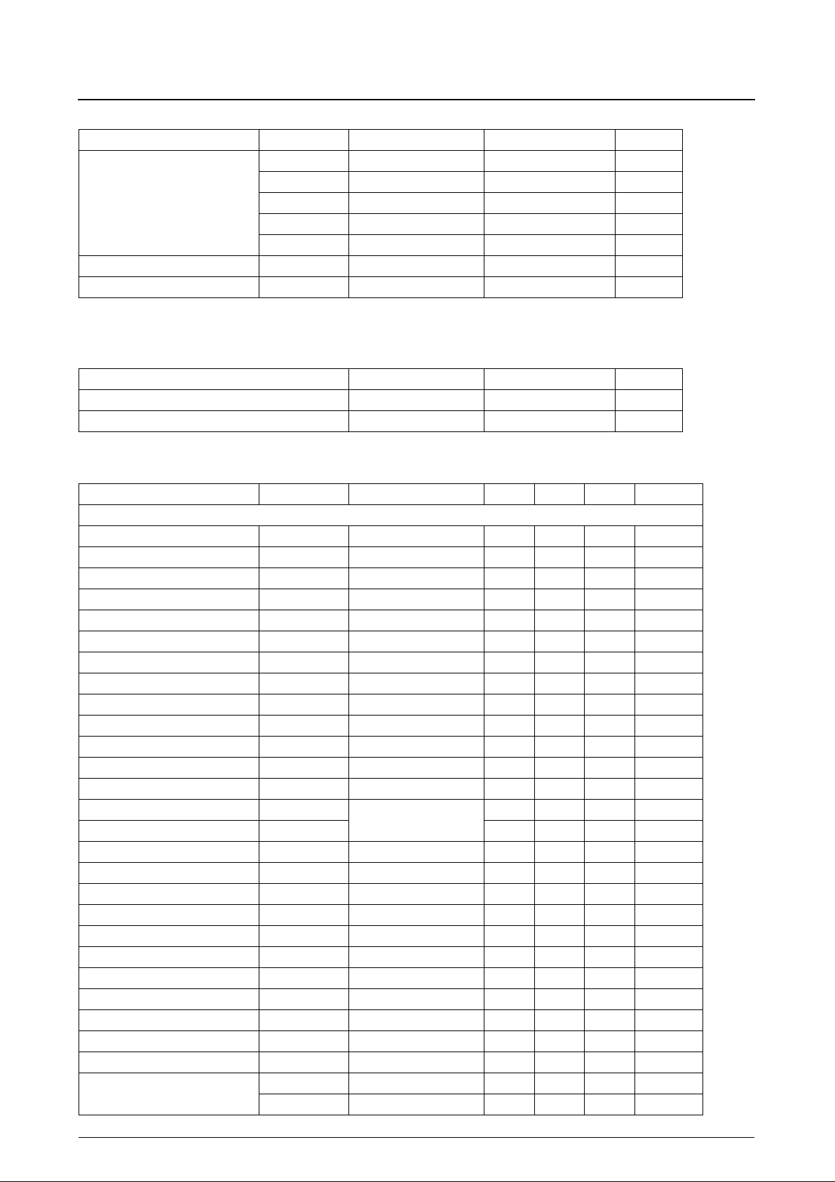
Parameter Symbol Conditions Ratings Unit
I
1
I
Circuit currents
1
Operating temperature range Topg V
17
I
21
I
22
I
10
CC
Storage temperature range Tstg
1. Current flowing into the IC is positive and current flowing out is negative.
LA7577N
= 9V, Ta = − 20 to +75 ° C
– −
−
∆
∆
−
−
1mA
10 mA
3mA
2mA
3mA
20 to +70 ° C
55 to +150 ° C
Recommended Operating Conditions
at Ta = 25 ° C
Parameter Symbol Ratings Unit
Supply voltage V
Operating supply voltage range V
Electrical Characteristics
at Ta = 25 ° C, V
CC
= 12V
CC
op 8.2 to 13.2 V
CC
9 or 12 V
Parameter Symbol Conditions min typ max Unit
[VIF]
Circuit current I
Quiescent video output voltage V
Maximum RF AGC voltage V
Minimum RF AGC voltage V
Quiescent AFT voltage V
Input sensitivity V
9
21
10H
10L
14
i
V
= 5V 44 55 68 mA
13
V
= 5V 6.6 7 7.4 V
13
V
= 7V 10.6 11 11.4 V
13
V
= 7V – 0 0.5 V
13
V
= 5V 3.0 5.9 8.0 V
13
33 39 45 dB/ µ V
AGC dynamic range GR 59 65 – dB
Maximum allowable input V
Video output amplitude V
max 100 105 – dB/ µ V
i
(video) 1.95 2.25 2.55 Vp-p
o
Output signal-to-noise ratio S/N 49 55 – dB
Sync signal tip voltage V
920kHz beat level l
Frequency characteristic f
Differential gain DG
Differential phase DP – 2 5 deg
Maximum AFT voltage V
Minimum AFT voltage V
White-noise threshold voltage V
White-noise clamp voltage V
Black-noise threshold voltage V
Black-noise clamp voltage V
AFT detector sensitivity S
VIF-stage input resistance R
VIF-stage input capacitance C
APC pull-in range (U) f
APC pull-in range (L) f
VCO maximum variation range
(tip) V
21
920
C
14H
14L
WTH
WCL
BTH
BCL
f
(VIF) f = 58.75MHz 0.8 1.3 1.75 k Ω
i
(VIF) f = 58.75MHz – 3.0 6.0 pF
i
PU-2
PL-2
f
U
f
L
= 10mV 4.15 4.45 4.75 V
i
P = 0, C = − 4dB, S = − 14dB 37 43 – dB
P = 0, S = − 14dB 6 8 – MHz
V
= 10mV, 87.5% mod,
i
f
= 58.75MHz
P
–36%
11 11.5 12 V
0 0.4 1.0 V
8.9 9.3 9.7 V
5.3 5.7 6.1 V
3.4 3.7 4.0 V
5.3 5.7 6.1 V
44 60 84 mV/kHz
0.6 1.6 – MHz
1.6
V
= 3V 0.6 1.6 – MHz
18
V
= 7V –
18
1.6
0.8 MHz
0.8 MHz
No. 4037—2/16
Page 3
β
LA7577N
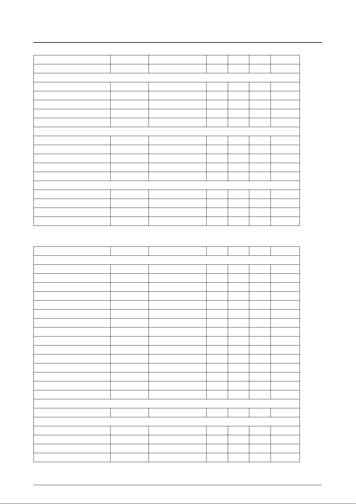
Parameter Symbol Conditions min typ max Unit
VCO control sensitivity
[1st SIF]
4.5MHz conversion gain VG 21 26 31 dB
4.5MHz output level V
1st SIF stage maximum input V
1st SIF stage input resistance R
1st SIF stage input capacitance C
SIF1
max +2.2dB, − 1dB 60 70 - mVrms
SIF
(SIF1) f = 54.25MHz 1.2 2 2.7 k Ω
i
(SIF1) f = 54.25MHz – 3 6 pF
i
[SIF]
SIF limiting sensitivity V
FM detector output voltage V
(lim) V
i
o
AM rejection AMR V
Total harmonic distortion THD V
SIF signal-to-noise ratio S/N (SIF) V
[Mute, Defeat]
AFT defeat start voltage V
AV mute threshold V
FM mute threshold V
AFT defeat voltage V
D11
4TH
2TH
D14
V
= 4.6 to 5V 1.5 3.1 6.2 kHz/mV
18
V
= 10mVrms 50 75 110 mVrms
i
= 5V – 33 39 dB/ µ V
13
V
= 5V 400 600 790 mVrms
13
= 5V 40 49 – dB
13
= 5V – 0.5 1.0 %
13
= 5V 60 78 – dB
13
0.5 2.3 – V
0.5 1.9 – V
0.5 2.0 – V
5.4 6 6.6 V
Electrical Characteristics
at Ta = 25 ° C, V
Parameter Symbol Conditions min typ max Unit
[VIF]
Circuit current I
Quiescent video output voltage V
Maximum RF AGC voltage V
Minimum RF AGC voltage V
Quiescent AFT voltage V
Input sensitivity V
Video output amplitude V
Sync signal tip voltage V
Maximum AFT voltage V
Minimum AFT voltage V
White-noise threshold voltage V
White-noise clamp voltage V
Black-noise threshold voltage V
Black-noise clamp voltage V
AFT detector sensitivity S
[SIF]
FM detector output voltage V
[Mute, Defeat]
AFT defeat start voltage V
AV mute threshold V
FM mute threshold V
AFT defeat voltage V
= 9V
CC
V
9
21
10H
10L
14
i
(video) 1.5 1.75 2.0 Vp-p
o
(tip) V
21
14H
14L
WTH
WCL
BTH
BCL
f
o
D11
4TH
2TH
D14
= 5V 39 48 59 mA
13
V
= 5V 5.0 5.4 5.8 V
13
V
= 7V 7.6 8 8.4 V
13
V
= 7V – 0 0.5 V
13
V
= 5V 2.6 4.5 6.0 V
13
37 43 49 dB/ µ V
= 10mV 3.25 3.55 3.85 V
i
8 8.5 9.0 V
– 0.3 1.0 V
6.8 7.2 7.6 V
4.0 4.4 4.8 V
2.5 2.8 3.1 V
2.5 4.1 4.5 V
28 39 55 mV/kHz
V
= 5V 400 600 790 mVrms
13
0.5 1.6 – V
0.5 1.1 – V
0.5 1.9 – V
3.9 4.5 5.1 V
No. 4037—3/16
Page 4
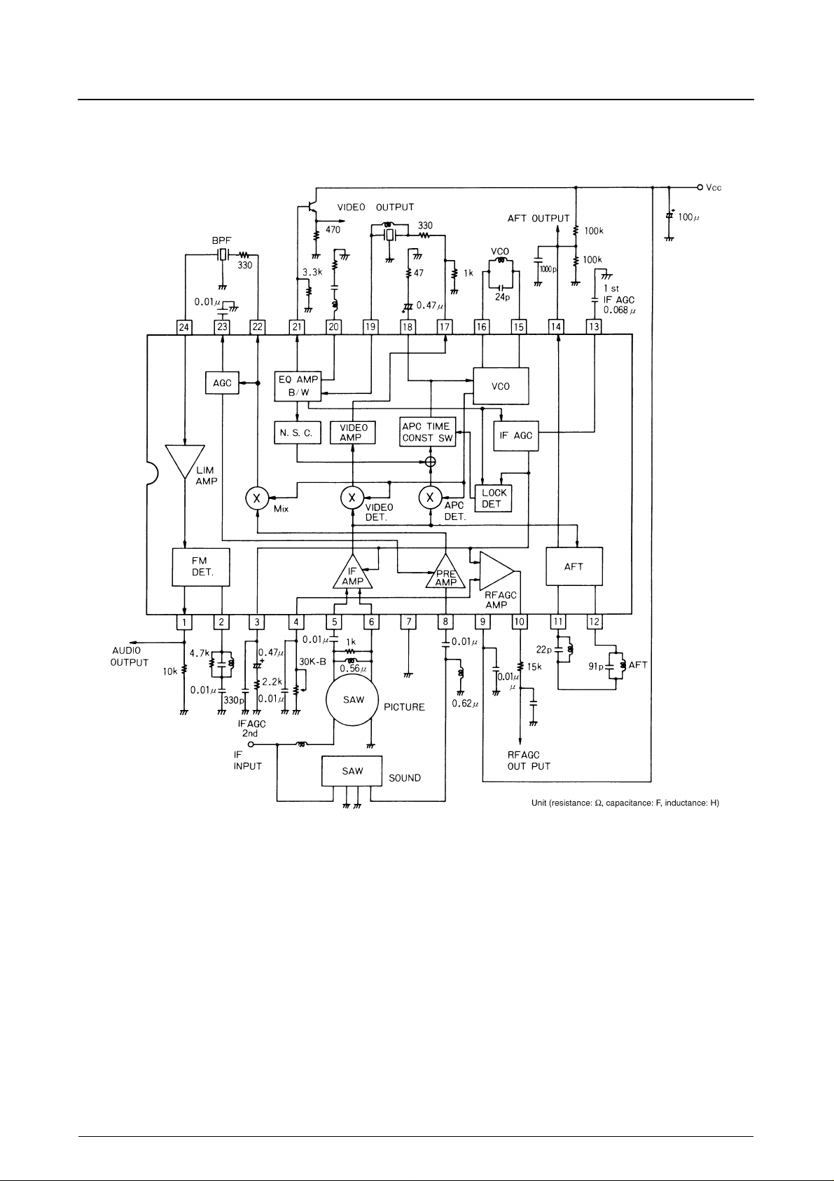
Sample Application Circuit (Japan)
LA7577N
No. 4037—4/16
Page 5
LA7577N
Sample Application Circuit (Japan)
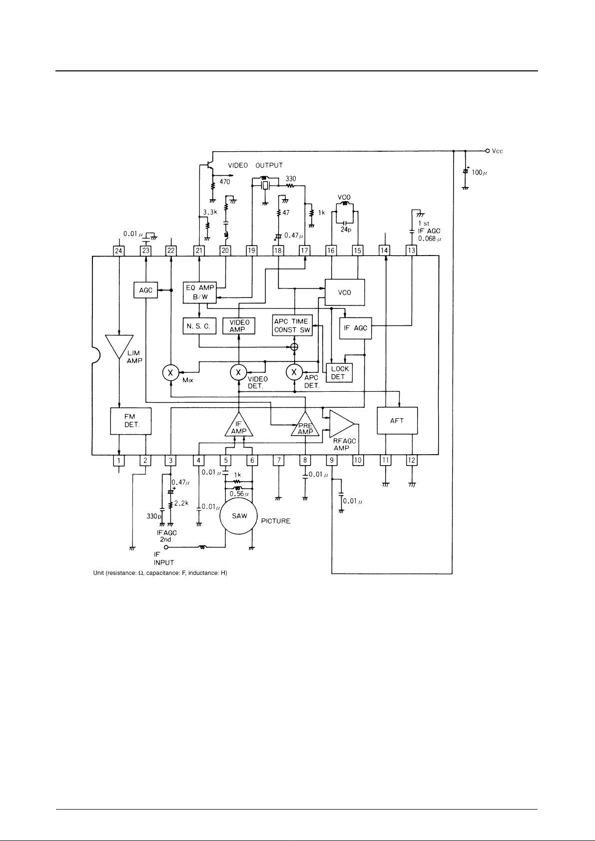
(when the SIF, 1st SIF, AFT and RF AGC are not used)
When the SIF stage is not used
• Leave pin 1 open
• Tie pin 2 to GND
• Leave pin 24 open
When the 1st SIF stage is not used
• Connect a 0.01µF capacitor between pin 8 and GND (leave the 0.01µF capacitor on pin 23 connected to GND)
• Leave pin 22 open
When the AFT circuit is not used
• Tie pins 11 and 12 to GND
• Leave pin 14 open
When the RF AGC circuit is not used
• Connect a 0.01µF capacitor between pin 4 and GND
• Leave pin 10 open
No. 4037—5/16
Page 6
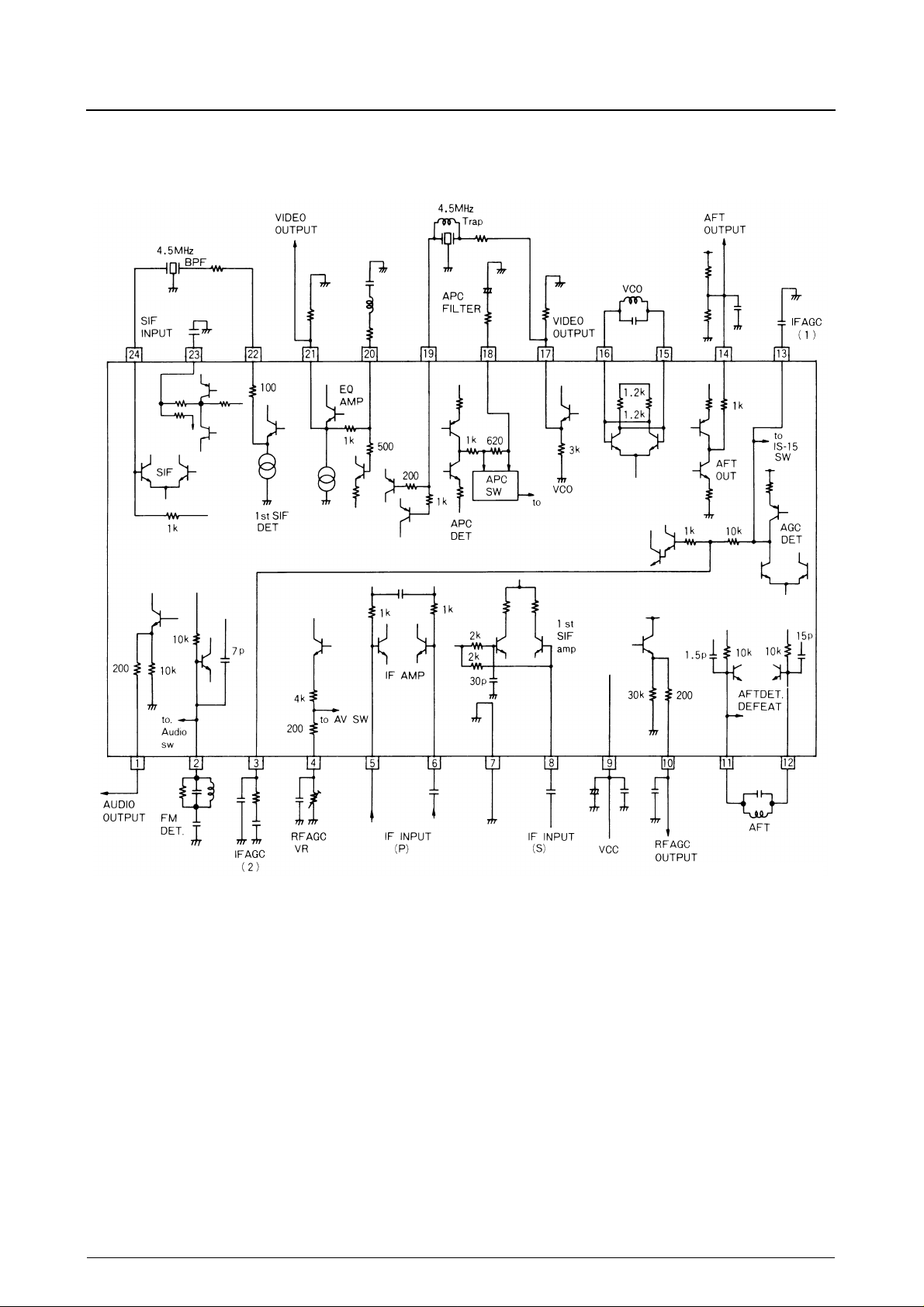
LA7577N Interface Circuit
LA7577N
No. 4037—6/16
Page 7
Buzz Canceler
LA7577N
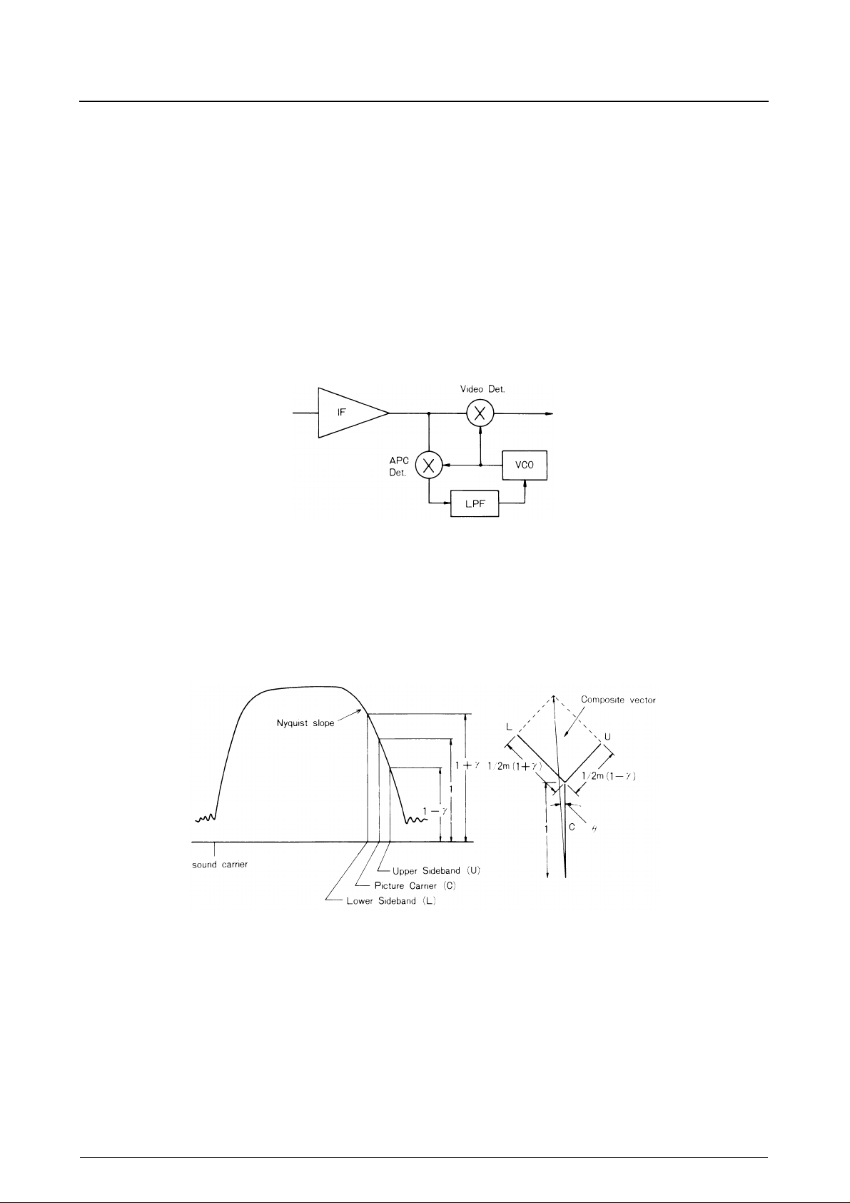
Phase-locked loop (PLL) detectors feature lower harmonic
distortion in the video stage, higher IF phase differential
suppression and much lower audio buzz than conventional
quasi-synchronous detectors. However, voltage-controlled
oscillators (VCO) in PLL detectors, generally, are highly
susceptible to interference from flyback pulses. This interference can affect the frequency of the VCO, resulting in
added output noise components and audio buzz. This
interference is minimized by VCO supply voltage regulation.
Figure 1. PLL detector
A simple PLL detector, however, can cause other audio
problems, because the broadcast signal is transmitted
using vestigial sideband modulation. In this case, the RF
signal is converted to an IF signal by the Nyquist slope of
the SAW filter. Since the sidebands in the vicinity of the
The PLL detector is shown in Figure 1. The automatic
phase control (APC) circuit multiplies the IF signal by the
VCO output signal, which is phase shifted by 90°, to suppress the AM component. The APC output is passed
through a low-pass filter to form the VCO control signal.
This results in a signal with a good carrier-to-noise ratio
(C/N).
picture carrier are attenuated, the magnitudes of the upper
and lower sideband vectors are different. The result is a
phase distortion component, θ,in the composite vector as
shown in Figure 2.
Figure 2. Phase noise component
No. 4037—7/16
Page 8
LA7577N
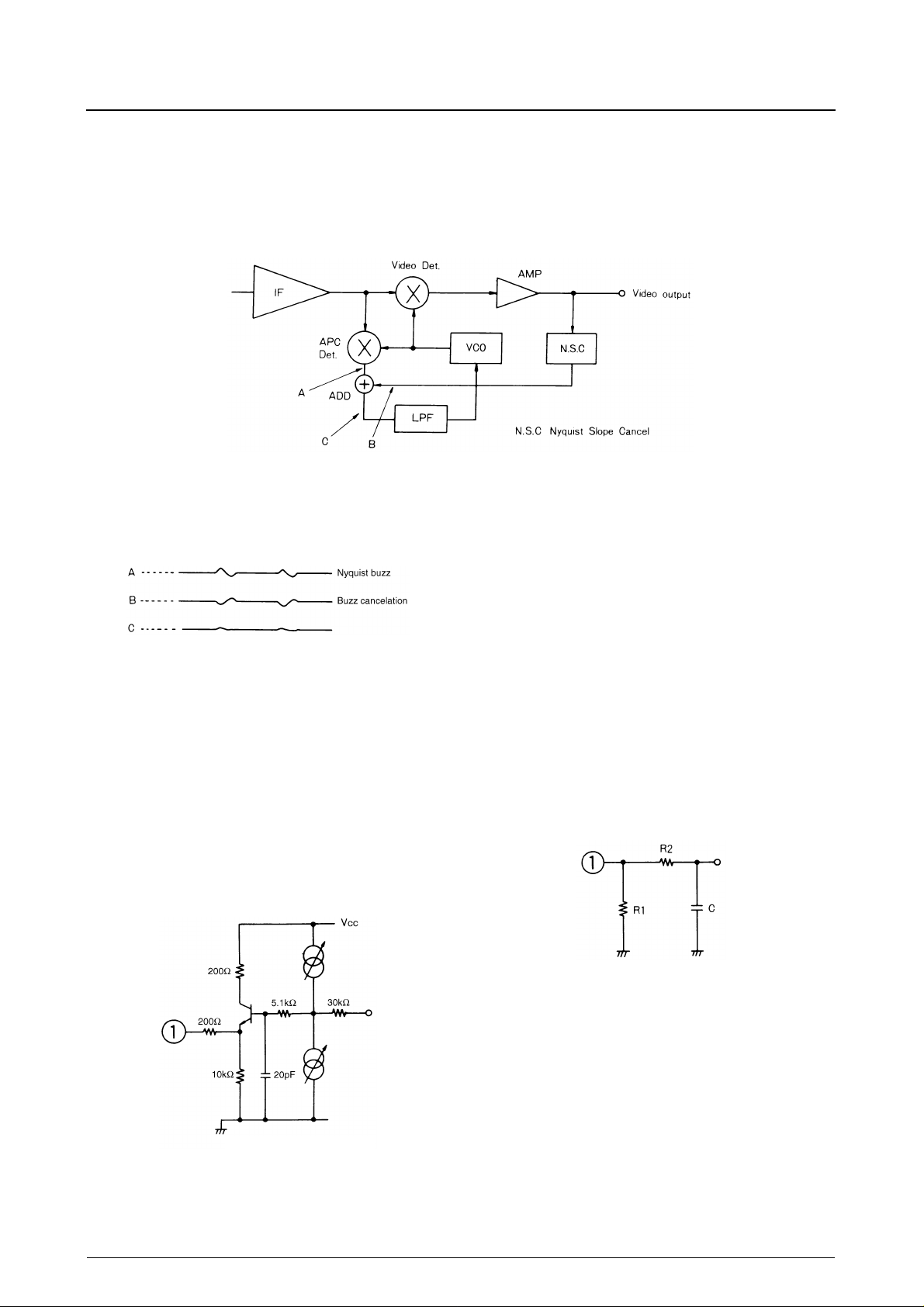
This phase distortion is the cause of audio buzz, or
Nyquist buzz, because the VCO synchronizes to the composite vector. A Nyquist buzz cancelation circuit is incorporated into the LA7577N to reduce the level of this noise
as shown in Figure 3.
Figure 3. PLL detector with buzz cancelation
A typical signal with Nyquist buzz is shown in Figure 4
together with the compensating signal generated by the
Nyquist-slope canceler and the resultant signal.
Figure 4. Nyquist buzz cancelation waveforms
Design Notes
FM Detector Output (Pin 1)
The FM detector output is an emitter follower with a
200Ω series protection resistor as shown in Figure 5.
In multiplex audio applications where pin 1 is connected
to the input of a multiplexed audio decoder, the input
resistance of the decoder can decrease, causing distortion
of the (L − R) signal. In this case, a 5.1kΩ or larger resistor, R1, should be connected between pin 1 and ground.
The circuit shown in Figure 3 is highly effective in suppressing audio buzz caused by the 4.5MHz IF beat signal
in Japanese multiplexed (L − R) audio or American (MTS)
Multichannel TV Sound (L − R) signals.
As buzz cancelation is independent of the PLL loop time
constant, other parameters such as automatic phase control
can be optimized to eliminate interference from flyback
pulses.
In monophonic applications, an RC de-emphasis circuit
should be connected as shown in Figure 6. The time constant is given by R2 × C.
Figure 5. FM detector output
Figure 6. RC de-emphasis circuit
No. 4037—8/16
Page 9
LA7577N
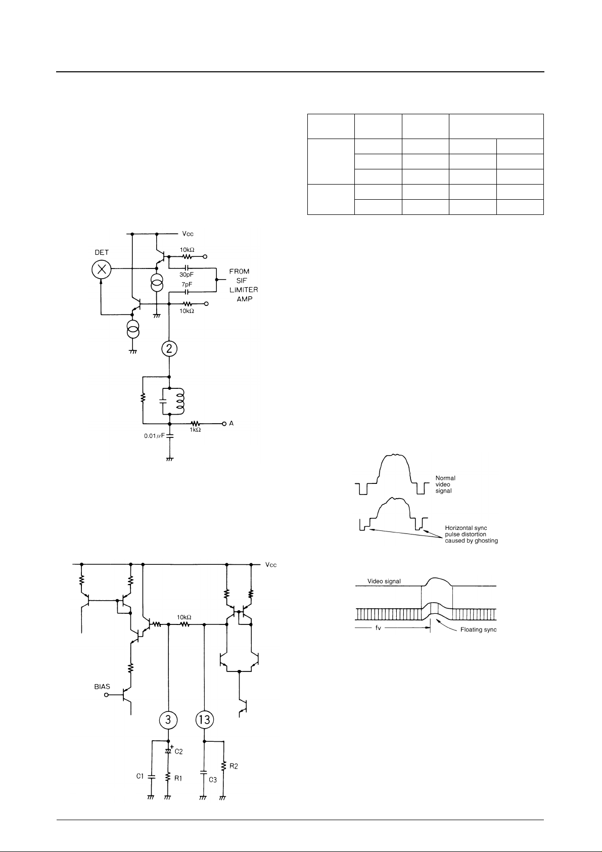
FM Discriminator (Pin 2)
The quadrature detector frequency at which the 90° phase
shift occurs is determined by the tuned circuit connected
to pin 2 as shown in Figure 7.
The detector bandwidth characteristics are determined
largely by the coil Q and damping resistance. The damping resistor should be chosen for the desired output level
and bandwidth characteristics.
FM muting is achieved by holding point A, in Figure 7, at
≤1V DC.
Typical AGC filter time constants
Pin Component
C1 330pF 330pF 330pF
3
13
R1 – 2.2k
C2 – 0.47µF 0.1µF
C3 0.47µF 0.068µF 0.047µF
R2 820k
Single time
constant
Ω
Double time constant
820k
Ω
Ω
1.8k
820k
Ω
Ω
Mute switch (IS-15 switch)
The black-noise canceler can be disabled by pulling pin 13
to 1V or lower. An external AGC source can then be
applied to pin 3 to drive the AGC circuit. This mode of
operation is designed for use with an IS-15 (EIA standard)
switch.
Ghosting problems
Reflected signals which have a phase different from that of
the main signal can cause distortion of the horizontal sync
pulse, as shown in Figure 9. As a result, the same chargeto-discharge current ratio of the IF AGC cannot be maintained. If the phase difference is large, the video signal can
also be distorted as shown in Figure 10. Distortion can be
minimized by connecting a 820kΩ to 1MΩ resistor
between pin 13 and ground.
Figure 7. FM discriminator
IF AGC (Pins 3 and 13)
The IF signal is peak detected and averaged by the filters
connected to pins 13 and 3, which are the 1st AGC and
2nd AGC, respectively, as shown in Figure 8. The IF AGC
audio component of the input signal to the video IF stage
is first removed by an audio trap.
Figure 9. Horizontal sync pulse distortion
Figure 10. Video signal distortion
Figure 8. IF AGC circuits
No. 4037—9/16
Page 10
LA7577N
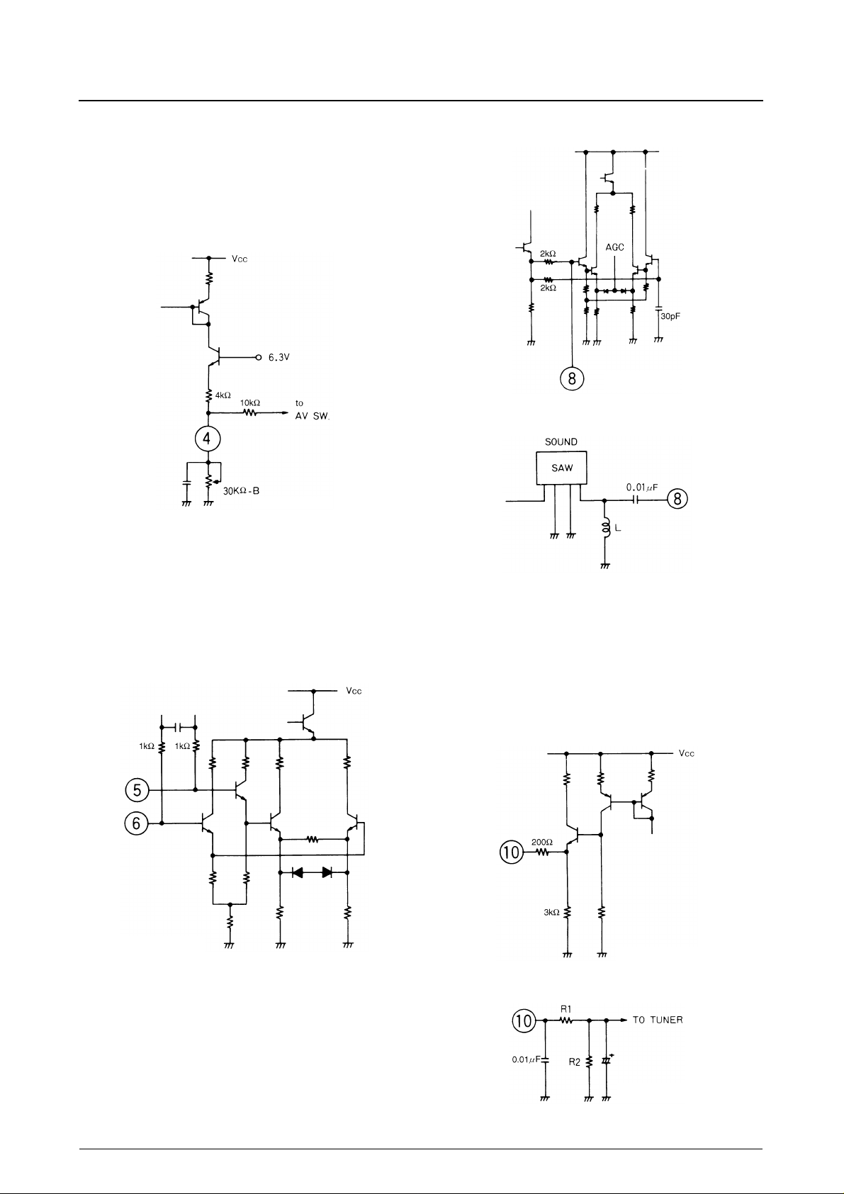
RF AGC Variable Resistor (Pin 4)
The operating point of the RF AGC can be adjusted using
a variable resistor connected to pin 4 as shown in Figure
11. When pin 4 is pulled to 0.5V or lower, both the FM
and video outputs are muted.
Figure 13. 1st SIF stage
Figure 11. RF AGC adjustment
VIF Input (Pins 5 and 6)
The VIF amplifier inputs on pins 5 and 6 should be capacitively coupled to block DC. The input signal is the average of the signals on these inputs. The input resistance is
approximately 1.5kΩ and the input capacitance is approximately 3pF.
Figure 14. SAW filter matching
RF AGC Output (Pin 10)
The RF AGC output on pin 10 is an emitter follower with a
200Ω series protection resistor as shown in Figure 15. The
value of the bleeder resistor connected between pin 10 and
the tuner, shown in Figure 16, should be chosen based on
the tuner maximum gain.
Figure 12. VIF stage
1st SIF Input (Pin 8)
The 1st SIF amplifier input on pin 8, shown in Figure 13,
should be capacitively coupled to block DC. If a SAW filter is used, an inductor should also be connected as shown
in Figure 14. This matches the SAW filter output capacitance to the LA7577N input capacitance and increases the
sensitivity. The inductor typically would be 0.62µH (for
Japan), 1.0µH (for the USA) or 1.3µH (for PAL countries).
Figure 15. RF AGC output
Figure 16. Bleeder resistor connection
No. 4037—10/16
Page 11
LA7577N
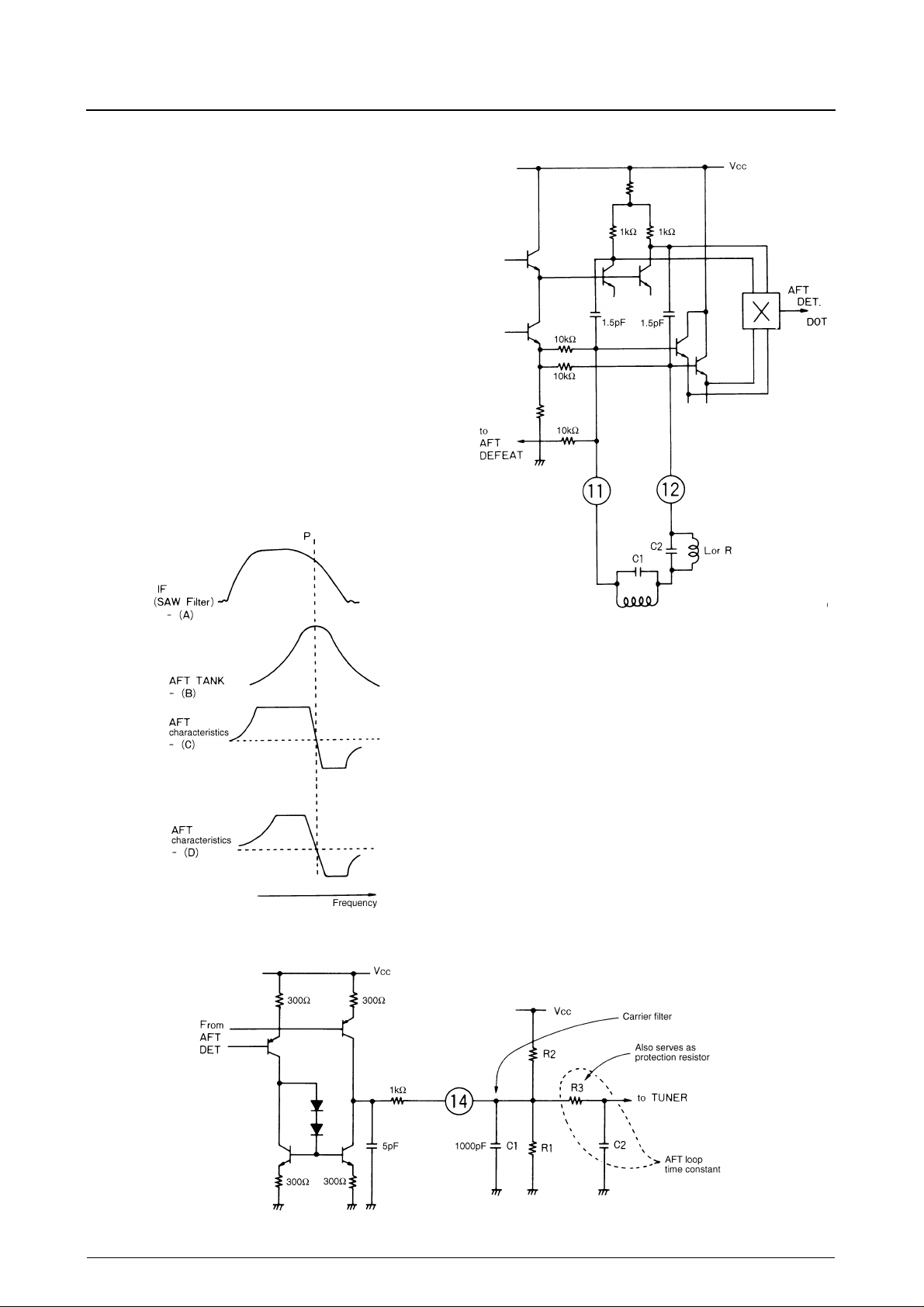
AFT Tank (Pins 11 and 12)
The automatic frequency tuner (AFT) tank connected to
pins 11 and 12 generates the 90° phase shift required for
quadrature detection. The band-pass frequency characteristics of the IF SAW filter and the AFT tank are shown in
Figure 17(A) and 17(B), respectively. The combined
response is shown in Figure 17(C). The resulting extended
low-frequency response, which increases susceptibility to
incorrect operation, can be reduced by connecting capacitor C2 in series with the AFT tank as shown in Figure 18.
The resultant frequency response is shown in Figure
17(D).
Capacitors C1 and C2 should have a ratio of approximately 5 to 1. An inductor or resistor should also be connected in parallel with C2 to maintain the DC balance of
the AFT tank.
The AFT can be defeated by connecting pin 11 to ground
through resistor R1, which should be 20kΩ or lower.
Figure 17. AFT tank characteristics
Figure 18. AFT tank
AFT Output (Pin 14)
An external bleeder resistor is required to generate the
AFT voltage. The AFT loop time constant is formed by
external resistor R3 and capacitor C2, as shown in Figure
19. The resistor also provides overvoltage protection.
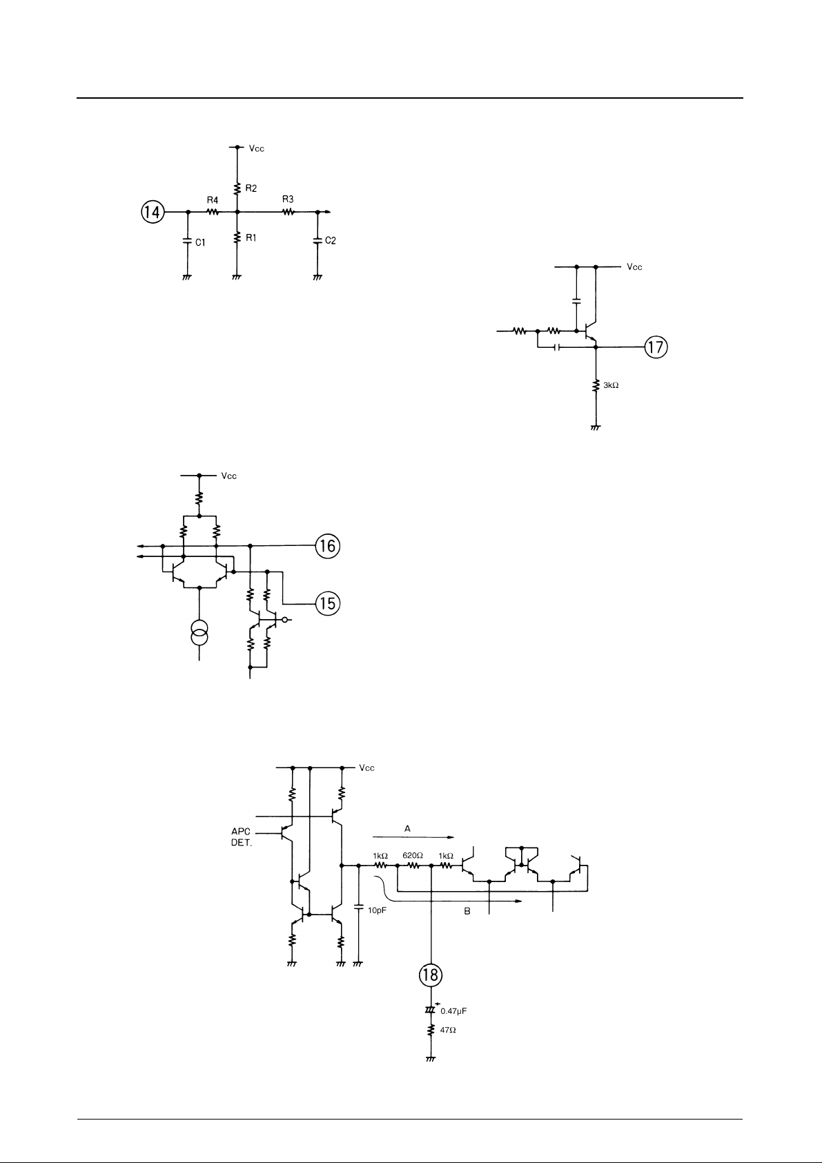
Fluctuations in the AFT quiescent output voltage, if
present in station selector systems using PLLs or voltage
synthesizers, can be reduced by connecting series resistor
R4 as shown in Figure 20. Note, however, that this also
reduces the AFT range.
Figure 19. AFT loop time constant
No. 4037—11/16
Page 12
LA7577N
Figure 20. AFT output
VCO Tank (Pins 15 and 16)
The VCO tank circuit is shown in Figure 21. The tank circuit capacitors connected between pins 15 and 16 should
be in the range 20 to 27pF (24pF is recommended). The
VCO tank susceptibility to external effects can be reduced
by using either chip capacitors or capacitors integrated
with the tank coil.
Composite Video Output (Pin 17)
The 4.5MHz composite video output circuit is shown in
Figure 22. A resistor should be connected between this
emitter-follower output and ground to ensure adequate
output drive capability. The resistor should be ≥1.2kΩ
(VCC = 12V), or ≥1kΩ (VCC = 9V).
Figure 22. Composite video output
APC Filter (Pin 18)
Figure 21. VCO tank
Time-constant switching is incorporated into the VCO for
automatic phase control (APC). When the PLL is locked,
the VCO is controlled by loop A, shown in Figure 23.
When the PLL is unlocked or the signal is weak, the VCO
is controlled by loop B which has higher gain. The
increased APC loop gain also increases the pull-in range.
The recommended range for the external APC filter resistor is 47 to 150Ω, and for the capacitor, 0.47µF.
Figure 23. APC filter
No. 4037—12/16
Page 13

LA7577N
Figure 24. Equalization amplifier
Equalization Amplifier (Pins 19 to 21)
The video signal, after passing through the 4.5MHz trap, is
input on pin 19 to the equalization amplifier, and output on
pin 21. A resistor should be connected between the emitter-follower output and ground to ensure adequate output
drive capability. The resistor should be ≥2.7kΩ (VCC =
12V) or ≥2.2kΩ (VCC = 9V). A buffer transistor should be
used if the signal is taken off-board.
Equalization amplifier design
The equalization amplifier has an external series resonant
circuit, shown in Figure 24, which controls the frequency
characteristic. The output voltage, Vo, is given by the following equation:
Vo = (R1/Z + 1) (Vi + Vin)
Since the input voltage, Vin, is small, the gain is given
approximately by the following equation:
AV = Vo/Vi = R1/Z + 1
The amplifier can be used as a voltage amplifier by connecting a network to pin 20 as shown in Figure 25. The
bleeder resistor should be chosen to avoid excessive gain
and extreme video sync tip voltages.
External bleeder resistor selection
If the equalization amplifier is configured for non-unity
gain, bleeder resistors R2 and R3, shown in Figure 26, are
required to ensure that the output DC voltage does not
change.
The sync tip voltage does not change if VX is approximately equal to V21. VX is given by the following equation:
VX = VCC × R2/(R2 + R3)
The voltage gain is given by:
AV = 1 + 1000/Z1
where
Z1 = R2 × R3/(R2 + R3)
and resistors R2 and R3 are given by:
R2 = 1000 × VCC/[(VCC − VX) × (AV − 1)]
R3 = 1000 × VCC/[VX × (AV − 1)]
Figure 25. Voltage amplifier configuration
Figure 26. External bleeder resistor circuit
No. 4037—13/16
Page 14
LA7577N
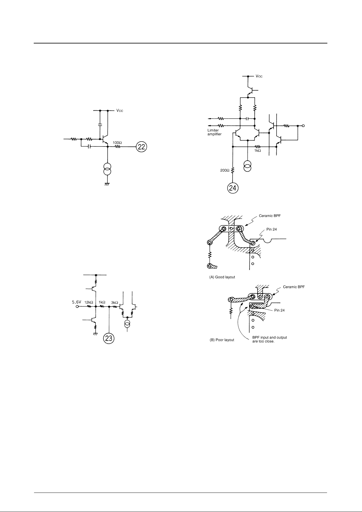
1st SIF Output (Pin 22)
The 1st SIF output is an emitter follower with internal
100Ω series resistor as shown in Figure 27. An additional
series resistor should be used for impedance matching to
the ceramic band-pass filter.
Figure 27. 1st SIF output
Figure 29. SIF stage input circuit
1st SIF AGC Filter (Pin 23)
The 1st SIF amplifier has an AGC range of approximately
30dB. The capacitor on pin 23 is normally 0.01µF, but
may, depending on the situation, be as large as 4.7µF
(4.7µF is recommended when using the filter for NICAM
signal processing).
Figure 28. 1st SIF AGC filter
SIF Input (Pin 24)
The input impedance of the amplifier, shown in Figure 29,
is approximately 1kΩ. Any interference on pin 24, a video
signal for example, can cause audio buzz or heterodyning.
Good circuit board layout is essential. Examples of both
good and poor layout are shown in Figure 30.
Figure 30. PCB layout examples
No. 4037—14/16
Page 15
LA7577N
Sanyo SAW Filters
Two types of surface acoustic wave (SAW) filter built on
different piezoelectric substrates can be used with the
LA7577N—Lithium Tantalate and Lithium Niobate.
Lithium T antalate (LiTaO3) SAW filters
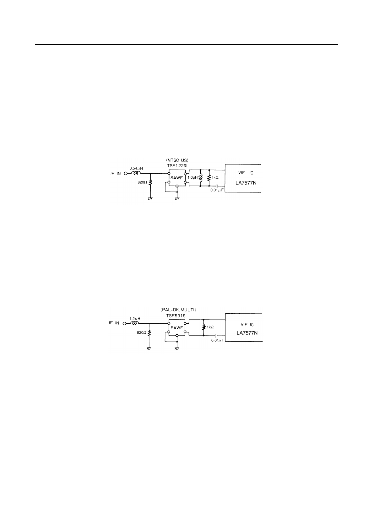
LiTaO3 SAW filters have a low temperature coefficient of
−18ppm/°C and good stability, but have high insertion
loss. An external coil is required at the output for level
matching as shown in Figure 31.
Figure 31. LiTaO
Lithium Niobate (LiNbO3) SAW filters
LiNbO3 SAW filters have a relatively high temperature
coefficient of −72ppm/°C, but have an insertion loss
approximately 10dB lower than LiTaO3 filters. A matching
circuit is, therefore, not required at the output, as shown in
Figure 32. As a result of the lower insertion loss, the passband ripple is higher. Ho wever, the lo w impedance and lo w
feedthrough of these filters make them less susceptible to
LiTaO3 SAW filters cover the Japanese and American
bands, which both have relatively high IF frequencies.
These filters have part numbers of the form TSF1××× or
TSF2×××.
SAW filter
3
stray capacitance effects caused by external components
and PCB layout, resulting in greater stability.
LiNbO3 SAW filters cover the PAL and American bands,
which have relatively lower IF frequencies. These filters
have part numbers of the form TSF5×××.
Figure 32. LiNbO3 SAW filter
VCO T ank Circuit
VCO tank circuit with built-in capacitor
When the IC power supply is switched ON, the heat generated by the IC is conducted by the PCB, including into the
VCO tank. The tank coil legs effectively act as a heatsink
and the heat is dissipated, such that an insignificant amount
of heat is conducted into the VCO tank capacitor. As a
result, the effect on VCO drift is made smaller.
Even so, it is recommended that the inductor and capacitor
be chosen so that their temperature characteristics effectively cancel. Accordingly, it is preferable to use inductors
with low temperature coefficient cores and low temperature coefficient capacitors.
VCO tank circuit with external capacitor
If using an external capacitor, the heat generated by the
IC is conducted by the PCB, including to the external
capacitor. If this happens, the heat affects the capacitor
and changes its capacitance value.
However, because the VCO tank coil is not significantly
affected, the VCO tank tuning point changes.
In this case, it is highly preferable to use inductors with
low temperature coefficient cores and low temperature
coefficient capacitors.
No. 4037—15/16
Page 16
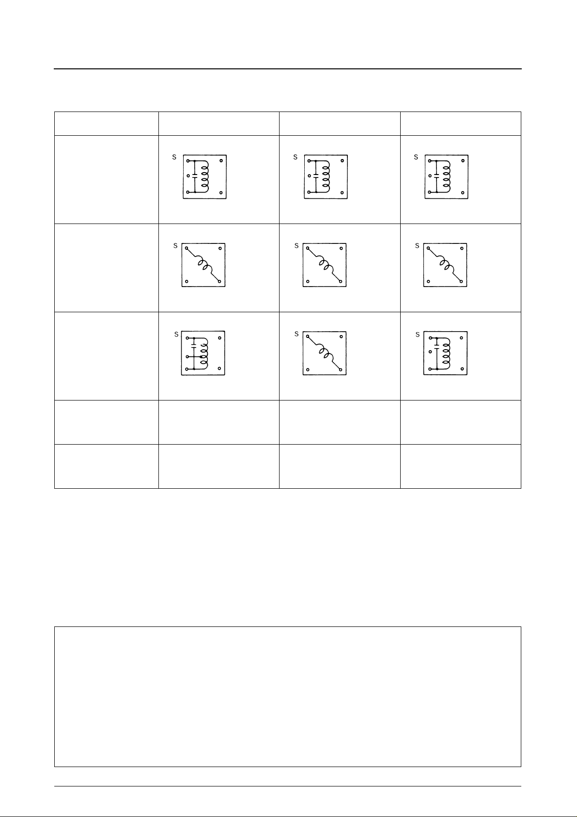
Coil Specifications
LA7577N
VCO coil
T
1
AFT coil
T
2
SIF coil
T
4
Component
Japan
f = 58.75MHz
6T
0.12
φ
C = 24pF
HW6226-4 HW6227-4 MA6389
3.5T
0.5
φ
MA8181 MA6343 MA7115
19T
0.08
φ
C = 100pF
KS6102-1 KS6102-1 MA8182
USA
f = 45.75MHz
9T
0.12
φ
C = 24pF
5.5T
0.5
φ
19T
0.08
φ
C = 100pF
PAL countries
f = 38.9MHz
11T
0.12
φ
C = 24pF
7.5T
0.5
φ
25T
0.08
φ
C = 100pF
VIF SAW filter (Sanyo) TSF1132L, TSF1137U TSF1229L, TSF1241U TSF5315
SIF SAW filter (Sanyo) TSB1101P TSB1205P –
■
No products described or contained herein are intended for use in surgical implants, life-support systems, aerospace equipment, nuclear
power control systems, vehicles, disaster/crime-pre v ention equipment and the lik e, the failure of which may directly or indirectly cause injury,
death or property loss.
■
Anyone purchasing any products described or contained herein for an above-mentioned use shall:
➀
Accept full responsibility and indemnify and defend SANYO ELECTRIC CO., LTD., its affiliates, subsidiaries and distributors and all their
officers and employees, jointly and severally, against any and all claims and litigation and all damages, cost and expenses associated
with such use:
➁
Not impose any responsibility for any fault or negligence which may be cited in any such claim or litigation on SANYO ELECTRIC CO.,
LTD., its affiliates, subsidiaries and distributors or any of their officers and employees, jointly or severally.
■
Information (including circuit diagrams and circuit parameters) herein is for e xample only; it is not guaranteed for volume production. SANYO
believes information herein is accurate and reliable, but no guarantees are made or implied regarding its use or any infringements of
intellectual property rights or other rights of third parties.
This catalog provides information as of June, 1997. Specifications and information herein are subject to change without notice.
No. 4037—16/16
 Loading...