

Page 1

Features
■ For air and liquid cooled applications
■ Ambient air temperature (thermistor)
compensated
■ Special default compensation curve with TS-
terminal open
■ Compensation curve with application specific
resistor on TS
■ Thermal protection
■ Field driver, lamp driver, relay driver, and df
(field monitor) short circuit protected
■ Load response control
■ Single phase autostart
L9484
Alternator voltage regulator
Multiiwatt8
Description
The L9484 is a monolithic multifunction alternator
voltage regulator intended for use in automotive
charging applications.
Table 1. Device summary
Order code Package Packing
L9484 Multiwatt8 Tube
L9484 regulates the output of an automotive
generator by controlling the field winding current
by means of a variable frequency PWM high side
driver.
November 2008 Rev 3 1/11
www.st.com
11
Page 2

L9484
Contents
1 Pin description . . . . . . . . . . . . . . . . . . . . . . . . . . . . . . . . . . . . . . . . . . . . . 3
2 Electrical specification . . . . . . . . . . . . . . . . . . . . . . . . . . . . . . . . . . . . . . . 4
2.1 Absolute maximum ratings . . . . . . . . . . . . . . . . . . . . . . . . . . . . . . . . . . . . . 4
2.2 Thermal data . . . . . . . . . . . . . . . . . . . . . . . . . . . . . . . . . . . . . . . . . . . . . . . 4
2.3 Electrical characteristcs . . . . . . . . . . . . . . . . . . . . . . . . . . . . . . . . . . . . . . . 4
2.4 Diagnostic . . . . . . . . . . . . . . . . . . . . . . . . . . . . . . . . . . . . . . . . . . . . . . . . . . 7
2.5 Fault indication . . . . . . . . . . . . . . . . . . . . . . . . . . . . . . . . . . . . . . . . . . . . . . 7
2.6 Regulation features . . . . . . . . . . . . . . . . . . . . . . . . . . . . . . . . . . . . . . . . . . 7
3 Package information . . . . . . . . . . . . . . . . . . . . . . . . . . . . . . . . . . . . . . . . . 9
4 Revision history . . . . . . . . . . . . . . . . . . . . . . . . . . . . . . . . . . . . . . . . . . . 10
2/11
Page 3

L9484
1 Pin description
Table 2. Pin description
N # Pin Description
1V
Generator output – voltage sense and power supply to ASVR
GO
2 F+ Field driver - high side drive output
3 G Ground for ASVR (must be connected for ground for ASVR)
4 TS Thermistor sense terminal
Internally connected to the tab or slug in MW-8. Shall not be used for ASVR
5Gnd
ground, nor voltage applied to pin 5 to cause ≥ 50mV pin 5 to pin 3. May be
unconnected or externally connected to pin 3.
6 DF Inverted field monitor output
7 L Lamp - low side driver; relay - high side driver
8 P Phase sense input
Figure 1. Pin connection (top view)
8
7
6
5
4
3
2
1
P
L
DF
GND
TS
G
F+
V
GO
Tab connected to pin 5
D02AT502
3/11
Page 4

2 Electrical specification
2.1 Absolute maximum ratings
Table 3. Absolute maximum ratings
Symbol Parameter Value Unit
I
Output current capability Internally limited A
o
P
2.2 Thermal data
Table 4. Thermal data
Symbol Parameter Value Unit
T
T
R
th j-case
Power dissipation 6 W
tot
Short circuit protected
T
Junction temperature -40 to +150 °C
j
Storage temperature -50 to +150 °C
stg
Thermal shut-down 175 ± 15 °C
sd
Thermal resistance junction to case 1.5 °C/W
L9484
All terminal, to VGO
and ground
2.3 Electrical characteristcs
Table 5. Electrical characteristcs
(T
= -35°C to +150°C continuous unless otherwise specified)
case
Symbol Parameter Test condition Min. Typ. Max. Unit
V
V
V
V
V
Operating supply voltage T
OS
Operating supply voltage T
OS
I
Stand-by current
SB
Regulator set-point 10kΩ between VGO and TS Curve shown in Figure 3
SP
Regulator set-point
SP
Generator output, no
NB
battery
T
Thermal compensation voltage @ VGO
C
= +25°C to =150°C8 VovV
case
= -40°C to +25°C10 VovV
case
V
= 12.6V; T
GO
10kΩ V
to TS; F+, G & tab
GO
(slug) grounded; L, DF, & P
case
= 25°C;
300 μA
unconnected; regulator not
activated.
NTC thermistor with R
10kΩ; Tj = 90°C
No battery, I
= 2A to 50%
OUT
max. load
25°C
Curves shown in Figure 4
=
(with MURATA NTC
NTH4G39A1)
VSP -
2
VSP +
2
Curves shown in Figure 3
and Figure 4
V
4/11
Page 5
L9484
Table 5. Electrical characteristcs (continued)
(T
= -35°C to +150°C continuous unless otherwise specified)
case
Symbol Parameter Test condition Min. Typ. Max. Unit
V
V
V
V
I
F-LIM
I
F-LIM
I
G-MIN
V
I
F
V
I
DF-LK
F
TURBO
F
TURBO
1. The Field Drive capability shall not decrease as a function of temperature between 25°C and 150°C, at a
rate faster than -0.024A/°C (for example, Field Drive shall be capable of ≥7.2A at 100°C).
Load regulation 6500 grpm, 10% to 95% load 300 mV
LR
Speed regulation
SR
Output saturation voltage
F-ON
Output saturation voltage
F-ON
Field limit current
Field limit current
(1)
(1)
Min. generator current load
Field discharge diode IF = 6A, T
D-F
Diode reverse current VR = 20V 1 mA
D-R
oscillation frequency During LRC operation 340 400 460 Hz
OSC
DF saturation voltage IDF ≤ 10mA 0.8 V
DF
15A load, 2000 to 20,000
grpm
= 6A, VGO = 14.0V, T
I
F
case
=
25°C
= 5A, VGO = 13.5V, T
I
F
case
=
125°C
Current F+ Terminal to Gnd.
@ T
case
≤ 25°C
Current F+ Terminal to Gnd.
@ T
= +150°C
case
Current measured @
generator output
= 25°C1.85V
case
9.0 A
6.0 A
0.5 A
DF output leakage current VDF < 25V 10 μA
Internal clock frequency VDF = 32 - 35V; thru 2.2kΩ 4X Hz
IRD, SS, LRC rate VDF = 32 - 35V; thru 2.2kΩ÷ 16
100 mV
750 mV
850 mV
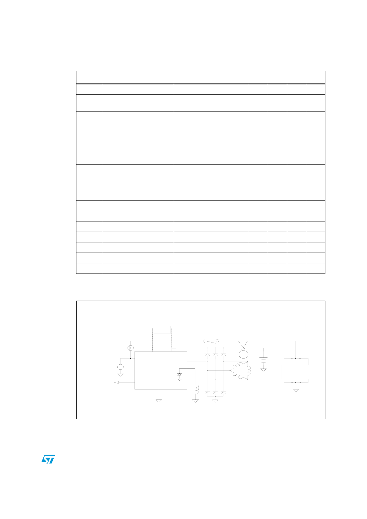
Figure 2. Typical application schematic
NTC
4
7
6
1
8
2
3
5/11
Page 6
L9484
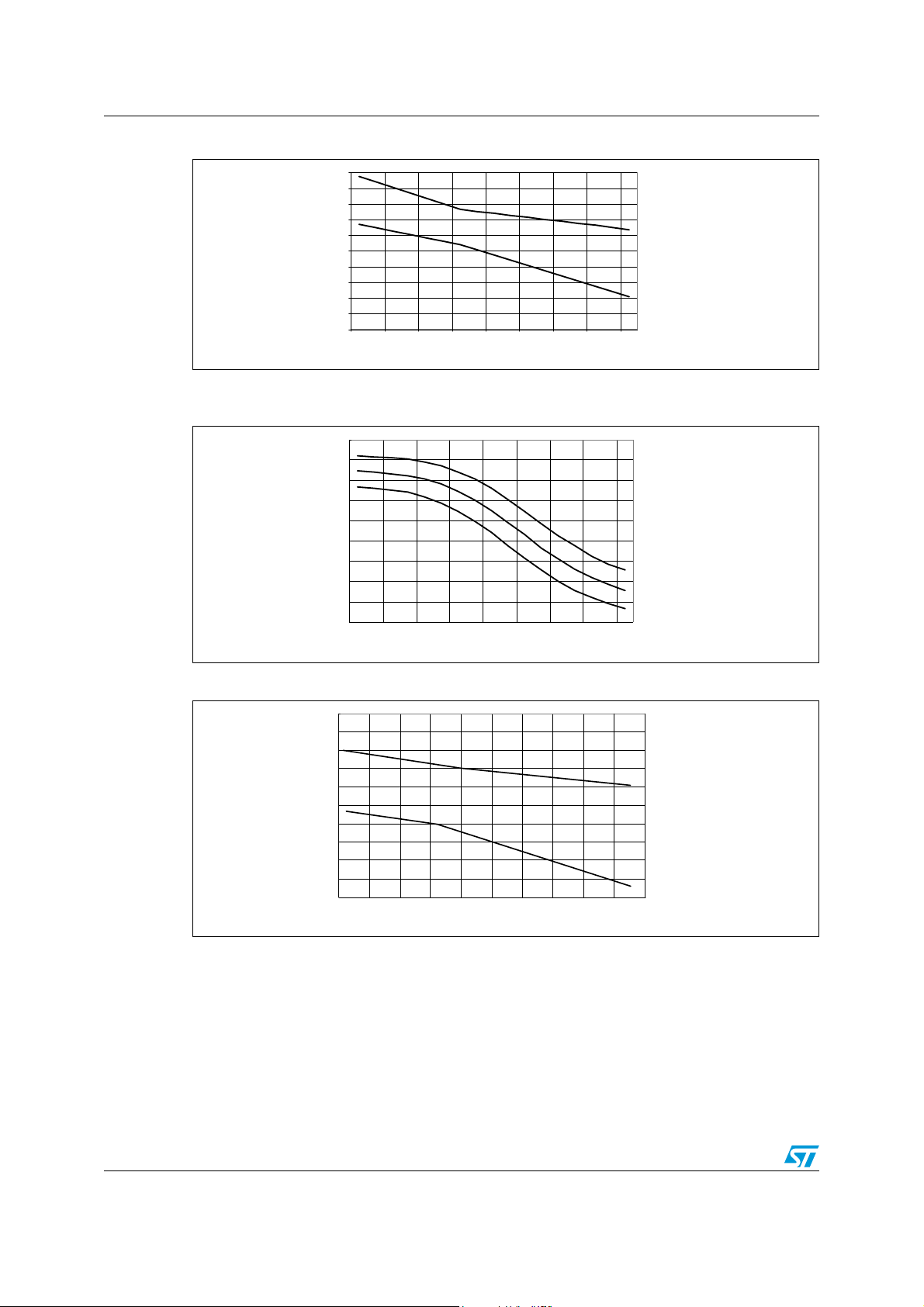
Figure 3. Set-point voltage vs. mounting tab temperature (10kΩ between VGO & TS)
15.5
15.3
15.1
14.9
14.7
14.5
Volts
14.3
14.1
13.9
13.7
13.5
-40 -20 0 20 40 60 80 100 120
Junction Temp
Figure 4. Set-point voltage vs. thermistor temperature, T
= 90°C (not guaranteed by
j
testing, depending on NTC characteristics)
15.2
15.04
15
14.8
14.73
14.6
14.4
Volts
14.2
14
13.8
13.6
13.4
-40 -20 0 20 40 60 80 100 120
14.88
14.49
13.91
13.53
NTC Temp
Figure 5. Set-point voltages vs. mounting tab temperature (TS-open)
15.2
15
14.80
14.8
14.6
14.4
14.12
14.2
14
Set Voltages
13.8
13.6
13.4
13.2
-40 -20 0 20 40 60 80 100 120
14.63
14.00
Tem p
14.43
13.36
160
140
6/11
Page 7
L9484
2.4 Diagnostic
Table 6. Diagnostic
(T
= -35°C to +150°C unless otherwise specified)
case
Symbol Parameter Conditions Min. Typ. Max. Units
+
V
SP
V
V
L-SAT
V
L-SAT-BO
V
L-RLY
T
DELAY
1. This condition can happen when the connection between the battery and VGO or the output terminal of the generator is
broken. The 1.1 second delay is not required, and current is sinked by ASVR.
2. When no fault is detected the Lamp terminal is pulled up by ASVR.
Over-voltage VSP + 1
OV
Lamp ON saturation voltage IL = 0.5A (sinked by ASVR) >V
Lamp ON voltage
(1)
Lamp OFF (relay drive)
saturation voltage (vs. B+)
IL < 0.5A, VGO = open; T
35°C to 85°C
IL = 750mA (sourced by
(2)
ASVR)
Tcase < 125C
case
= -
L-ACT
1.33 1.45 V
Fault indication delay time Delay before lamp ON 0.9 1.1 1.3 s
V
+ 2 V
1.3
SP
3.8 5 V
1.85 V
2.5 Fault indication
Table 7. Fault indication table
Conditions T
Initial KEY-ON Bulb and wiring check (lamp ON for 1 sec ± 15% after initial KEY-ON) No
VGO > V
V
F
No connection between battery and V
At start: lamp ON until F
P
< F
P
< V
OV
P-F
P-TR
AND VGO < V
@ V
P-TR
SP
P>FP-IR
GO
AND VP>V
. i.e. until VP reaches 8V. No
P-F
Delay
Ye s
Ye s
Ye s
No
?
2.6 Regulation features
Table 8.
Symbol Parameter Conditions Min. Typ. Max. Unit
V
L-PD
I
L-PD
V
P-IR
V
P-TR
Regulation features
L terminal regulator activate
threshold
L terminal pull down current
Initiate regulation phase voltage
threshold
Terminate regulation phase
voltage threshold
VGO=12.6V 0.8 1 1.15 V
VL = V
VGO=12.6V
L-ACT
0.09 0.78 mA
Regulator activated 1.1 1.3 1.5 V
Regulator activated 1.1 1.3 1.5 V
7/11
Page 8
L9484
Table 8.
Regulation features
(continued)
Symbol Parameter Conditions Min. Typ. Max. Unit
V
F
P-IR
F
P-TR
IRD Initiate regulation delay
Phase input voltage low fault
P-F
threshold
Phase terminal current sink
I
P
Initiate regulation phase
frequency
Terminate regulation phase
frequency
VP > 1.5V and < 12.6V
VGO = 12.6V
Regulator activated, V
conditions met first time.
F
P-IR
P-IR
AND
7.089.0V
0.3 3.5 mA
123 145 167 Hz
59 72 86 Hz
1.722.3s
Regulator activated and
FSDC Field strobe duty cycle
(regulation terminated or
16 18.75 22 %
regulation not initiated)
LRC Load response control rate Field drive duty cycle increase 34 40 46 %/s
F
P-LRC
SS Soft-start
LRC transition frequency LRC enabled if FP < F
LRC enabled until V
SP
regardless other conditions
P-LRC
reached
255 300 345 Hz
34 40 46 %/s
8/11
Page 9
L9484
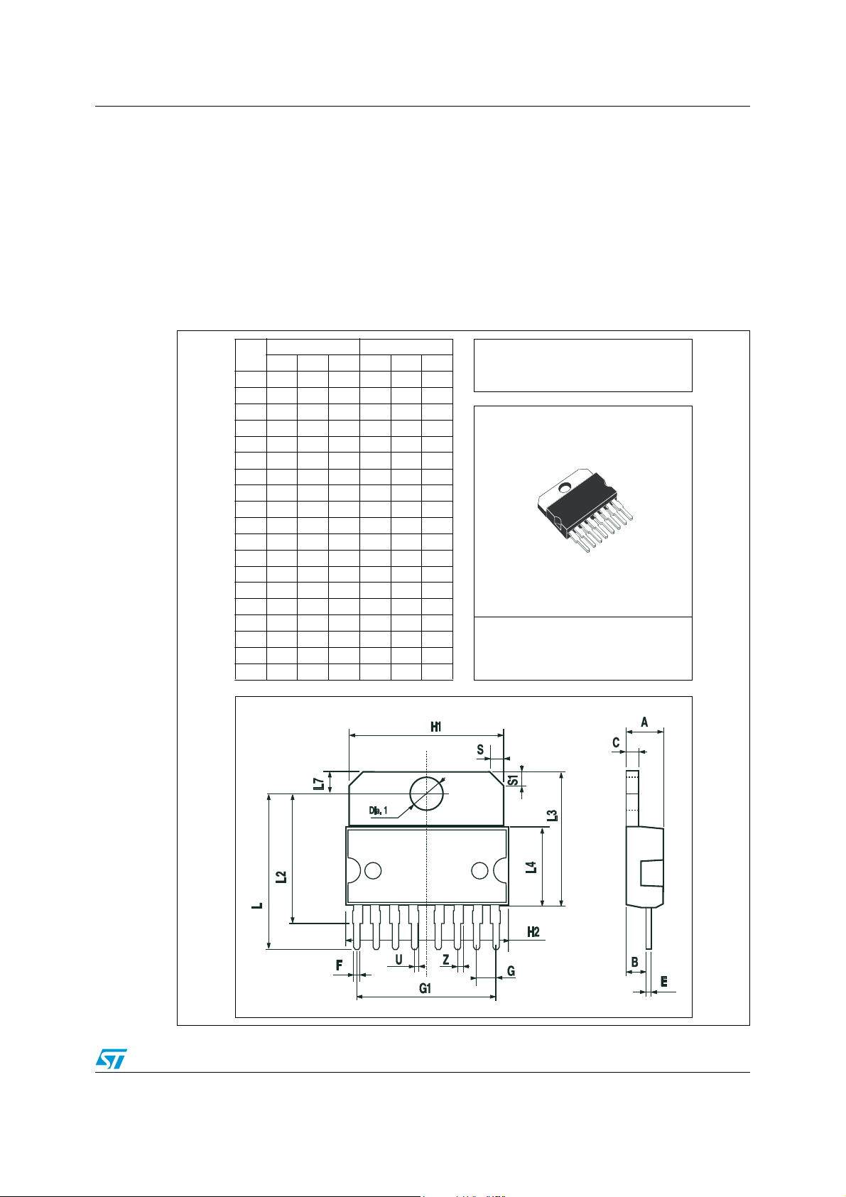
3 Package information
In order to meet environmental requirements, ST (also) offers these devices in ECOPACK®
packages. ECOPACK
®
packages are lead-free. The category of second Level Interconnect
is marked on the package and on the inner box label, in compliance with JEDEC Standard
JESD97. The maximum ratings related to soldering conditions are also marked on the inner
box label.
ECOPACK is an ST trademark. ECOPACK specifications are available at: www.st.com.
Figure 6. Multiwatt8 mechanical data and package dimensions
DIM.
A50.197
B 2.65 0.104
C1.60.063
E 0.49 0.55 0.019 0.022
F 0.78 0.85 0.030 0.033
G 2.40 2.54 2.68 0.094 0.10 0.105
G1 17.64 17.78 17.92 0.69 0 .70 0.71
H1 1 9.6 0.772
H2 20.2 0.795
L 20.35 20.65 0.80 0.81
L2 17.05 17.20 17.35 0.67 0 .68 0.68
L3 17.25 17 .5 17.75 0.679 0.689 0.699
L4 10.3 10.7 10.9 0.406 0.421 0.429
L7 2.65 2.9 0.104 0.114
S 1.9 2.6 0.075 0.102
S1 1.9 2.6 0.075 0.102
U 0.40 0.55 0.015 0.0 22
Z 0.70 0.85 0.028 0.034
Dia1 3.65 3.85 0.144 0.152
mm inch
MIN. TYP. MAX. MIN. TYP. MAX.
OUTLINE AND
MECHANICAL DATA
Multiwatt8 (Pin 5 GND)
0043696 F
9/11
Page 10
4 Revision history
Table 9. Document revision history
Date Revision Changes
15-Feb-2003 1 Initial release.
09-Sept-2004 2 Update
18-Nov-2008 3
L9484
Document reformatted.
Document promoted from “product preview” to “datasheet“.
Added Table 1: Device summary on page 1.
Added ECOPACK text in Section 3: Package information.
10/11
Page 11

L9484
Please Read Carefully:
Information in this document is provided solely in connection with ST products. STMicroelectronics NV and its subsidiaries (“ST”) reserve the
right to make changes, corrections, modifications or improvements, to this document, and the products and services described herein at any
time, without notice.
All ST products are sold pursuant to ST’s terms and conditions of sale.
Purchasers are solely responsible for the choice, selection and use of the ST products and services described herein, and ST assumes no
liability whatsoever relating to the choice, selection or use of the ST products and services described herein.
No license, express or implied, by estoppel or otherwise, to any intellectual property rights is granted under this document. If any part of this
document refers to any third party products or services it shall not be deemed a license grant by ST for the use of such third party products
or services, or any intellectual property contained therein or considered as a warranty covering the use in any manner whatsoever of such
third party products or services or any intellectual property contained therein.
UNLESS OTHERWISE SET FORTH IN ST’S TERMS AND CONDITIONS OF SALE ST DISCLAIMS ANY EXPRESS OR IMPLIED
WARRANTY WITH RESPECT TO THE USE AND/OR SALE OF ST PRODUCTS INCLUDING WITHOUT LIMITATION IMPLIED
WARRANTIES OF MERCHANTABILITY, FITNESS FOR A PARTICULAR PURPOSE (AND THEIR EQUIVALENTS UNDER THE LAWS
OF ANY JURISDICTION), OR INFRINGEMENT OF ANY PATENT, COPYRIGHT OR OTHER INTELLECTUAL PROPERTY RIGHT.
UNLESS EXPRESSLY APPROVED IN WRITING BY AN AUTHORIZED ST REPRESENTATIVE, ST PRODUCTS ARE NOT
RECOMMENDED, AUTHORIZED OR WARRANTED FOR USE IN MILITARY, AIR CRAFT, SPACE, LIFE SAVING, OR LIFE SUSTAINING
APPLICATIONS, NOR IN PRODUCTS OR SYSTEMS WHERE FAILURE OR MALFUNCTION MAY RESULT IN PERSONAL INJURY,
DEATH, OR SEVERE PROPERTY OR ENVIRONMENTAL DAMAGE. ST PRODUCTS WHICH ARE NOT SPECIFIED AS "AUTOMOTIVE
GRADE" MAY ONLY BE USED IN AUTOMOTIVE APPLICATIONS AT USER’S OWN RISK.
Resale of ST products with provisions different from the statements and/or technical features set forth in this document shall immediately void
any warranty granted by ST for the ST product or service described herein and shall not create or extend in any manner whatsoever, any
liability of ST.
ST and the ST logo are trademarks or registered trademarks of ST in various countries.
Information in this document supersedes and replaces all information previously supplied.
The ST logo is a registered trademark of STMicroelectronics. All other names are the property of their respective owners.
© 2008 STMicroelectronics - All rights reserved
STMicroelectronics group of companies
Australia - Belgium - Brazil - Canada - China - Czech Republic - Finland - France - Germany - Hong Kong - India - Israel - Italy - Japan -
Malaysia - Malta - Morocco - Singapore - Spain - Sweden - Switzerland - United Kingdom - United States of America
www.st.com
11/11
 Loading...