

Page 1
QUAD INTELLIGENT POWER LOW SIDE SWITCH
■
Quad power l ow side driver wi t h 2 x 5A and
2 x 3A output current capability
■
Low R
= 25°C
@ T
j
■
Internal output clamping structures with
V
= 50V for fast inductive load current
FB
typically 200mΩ and 300m
DSON
recirculation
■
Limited output voltage slew rate for low EMI
■
Protected µP compatible enable and input
■
Wide operati ng supply voltage ra nge 4.5 V to 32V
■
Real time diagnostic functions:
– Output shorted to GND
– Output shorted to V
SS
– Open load detection in ON and OFF condition
– Load bypass detection
– Overtemperature detection
■
Device protection functions:
– Overload disable
– Selective thermal shutdown
■
Signal- and Power-Ground-loss shutdown
Ω
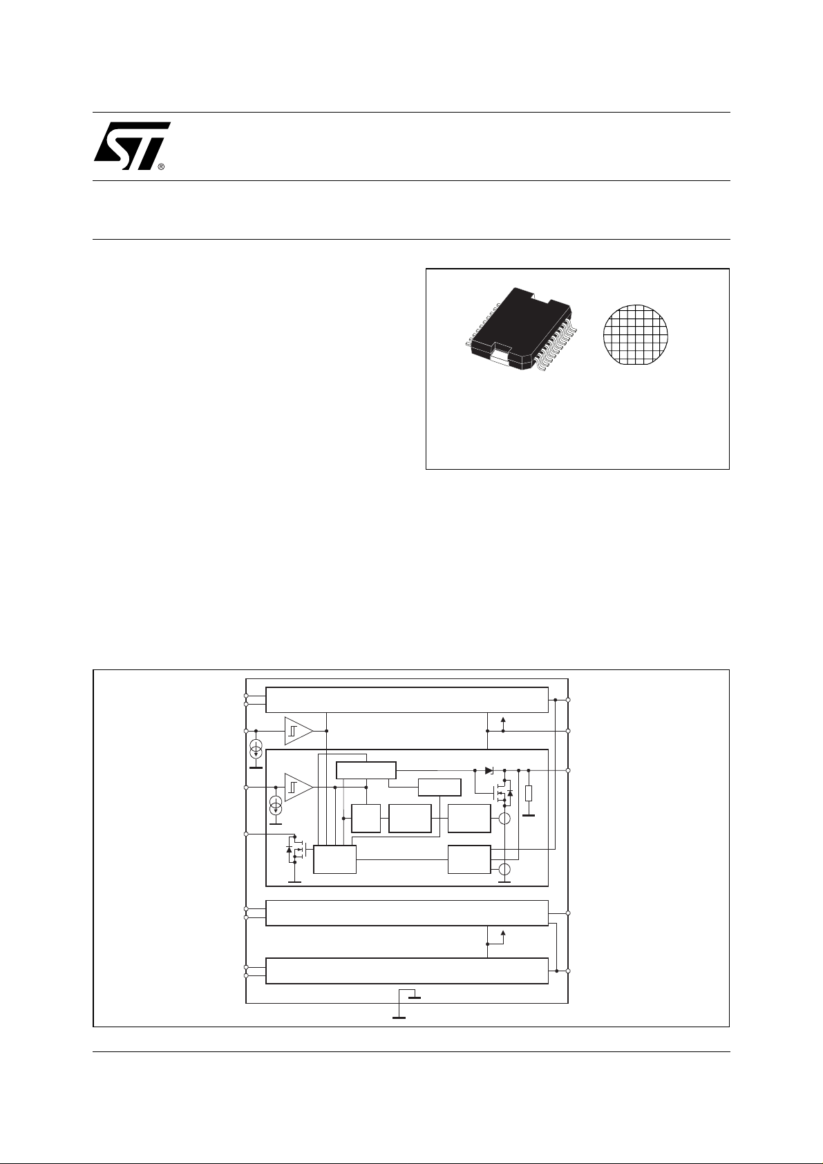
L9349
PowerSO20 BARE DIE
ORDERING NUMB ERS :
L9349 L9349DIE1
DESCRIPTION
The L9349 is a monolithic integrated quad low side
driver realized in an advanced M ultipowerBCD mixed
technology. The device is intended to drive valves in
automotive environment.
The inputs are µP compatible. Particular care has
been taken to protect the device against failures, to
avoid electromagnetic interferences and to offer extensive real time diagnostic.
BLOCK DIAGRAM
September 2002
IN1
D1
EN
IN4
D4
IN2
D2
IN3
D3
00AT0025
Output Control
Diagnostic
Control
R
QS
Channel 1
Delay
Time
Channel 4
Channel 2
Channel 3
GND
Overtemp
Overload
Openload
52V
OUT1
VS
OUT4
R
IO
OUT2
OUT3
1/12
Page 2
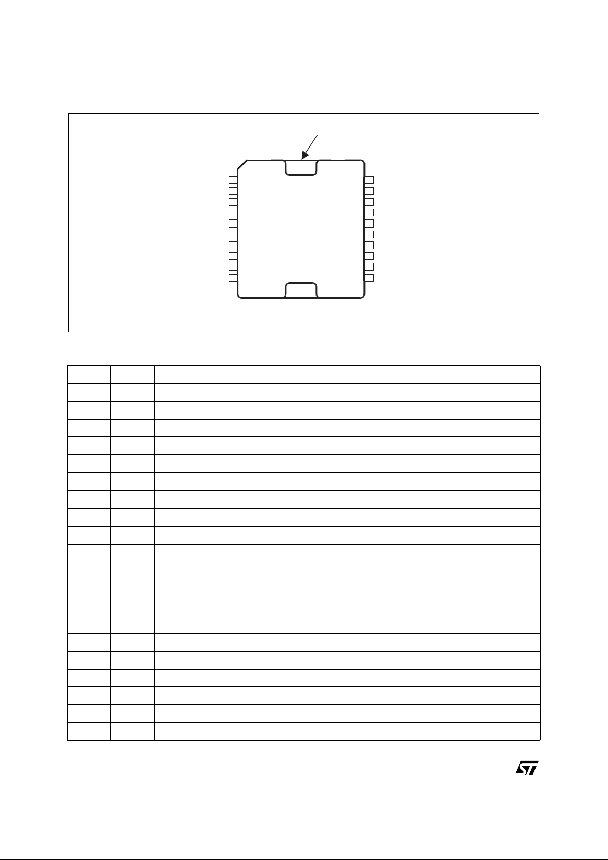
L9349
PIN CONNECTION
Heat sink connected
to pins 1, 10, 11, 20
PGND 1
OUT1 2
D1
3
IN4 4
VS 5
NC
6
IN3 7
D2 8
OUT2
9
PGND 10
00AT0026
PIN DESCRIPTION
N° Pin Function
1 PGND Power Ground
2 Out1 Output 1 (5A)
3 D1 Diagnostic 1
4 IN4 Input 4
5 VS Supply Voltage
20 PGND
OUT4
19
D418
IN117
EN
16
GND15
IN214
D3
13
OUT312
PGND11
6 NC Not Connected
7 IN3 Input 3
8 D2 Diagnostic 2
9 Out2 Output 2 (5A)
10 PGND Power Ground
11 PGND Power Ground
12 Out3 Output 3 (3A)
13 D3 Diagnostic 3
14 IN2 Input 2
15 GND Signal Ground
16 EN Common Enable
17 IN1 Input 1
18 D4 Diagnostic 4
19 Out4 Output 4 (3A)
20 PGND Power Ground
2/12
Page 3
THERMAL DATA
Symbol Parameter Value Unit
L9349
R
Th j-case
Thermal resistance junction to case 3 °C/W
ABSOLUTE MAXIMUM RATINGSI
Symbol Parameter Conditions Value Unit
V
V
SP
dVS/dt
V
IN, EN
V
V
ODC
I
O1, 2
I
O3, 4
I
OR1, 2
I
OR3, 4
E
O1, 2
E
O3, 4
V
∆
GND
T
jEO
T
T
stg
T
jDIS
ESD Electrostatical Discharging MIL883C +-2 kV
ESD OUT1 - 4 vs. Common-GND
DC Supply Voltage -0.3 to 32 V
S
Supply Voltage Pulse (duration <200ms) -0.3 to 45 V
Supply Voltage Slope 10
Input Voltage
Diagnostic DC Output Voltage
D
I
I
10mA
50mA
-1.5 to 6 V
-0.3 to 16 V
DC Output Voltage -0.3 to 45 V
DC Output Current Out 1, 2 5 A
DC Output Current Out 3, 4 3 A
Reverse Output Current -5 A
Reverse Output Current -3 A
Switch-off Energy for Inductive Loads
tEO = 250µs,
1)
50 mJ
T = 5ms 30 mJ
GND Potential Difference Tj = -40 to 150°C ±0.3 V
Junction Temperature During Switch-off
Junction Temperature -40 to T
j
Σt ≤
Σt ≤
30 min
15 min
175 °C
190 °C
jDIS
Storage Temperature -55 to 150 °C
Thermal Disable Junction Temp. Threshold 180 to 210 °C
+-4 kV
(PGNDs + GND)
V/µs
°C
1) tEO is the clamping time (see F i gure 1)
Electrical Characteristcs (Operating Range)
The electrical characteristics are valid within the below defined operating range, unless otherwise specified.
Symbol Parameter Test Condition Min. Typ. Max. Unit
V
T
T
1) Parameters guaranteed by corre l ation
Board Supply Voltage 4.5 12 32 V
S
Junction Temperature -40 150 °C
j1
Junction Temperature
j2
15min 1) over life time
Σt ≤
150 T
jDIS
°C
3/12
Page 4

L9349
g
ELECTRICAL CHARACTERISTICS
(V
= 4.5 to 32V; -40°C ≤ Tj1 ≤ 150°C < Tj2 ≤ T
S
jDIS
Symbol Parameter Test Conditions
Supply
I
VS OFF
I
VS ON
DC Supply Current Off EN = 1.0V 5 10 mA
DC Supply Current On
VS ≤ 14V; VIN, VEN = 2V
Diagnostic Outputs D1 - D4
V
Diagnostic Output Low
DL
≤ 3mA
I
D
Voltage
I
DLE
Diagnostic Output
Leakage Current
VD = 14V
1)
Outputs Out 1 - Out 4
R
DSON 1, 2
R
DSON 3, 4
Output On Resistance Tj = 25°C
T
= 150°C
j
VS > 9.5V I
Tj = 25°C
O1,2
Tj = 150°C
VS > 9.5V
I
= 1.3A
O3,4
, unless other-wise specified.)
Values T
Min. Typ. Max. Min. Max.
8mA
0.65 1.0 1.5 V
0.1 2 20
200 300
= 2A
300 450
j1
Values T
j2
Unit
A
µ
m
Ω
500
m
Ω
750
V
Z
R
O
V
OUV 1-4
V
OUV hys 1-
4
∆
V
OUV 1-4,
2-3, 4-1, 3-2
Z-diode clamping
e
volta
Output pull down
resistor
Open Load Voltage
I
≥ 200mA
OCL
VS > 9.5V
EN = 0V
VIN = 1V 0.525 x
Threshold
Hysteresis 0.003 x
Open Load Difference
Voltage Thres hold
V
IN1,4/2,3
= 1V VS ≤ 16V
VOc Š 4.5V
= output voltage of
V
OC
45 60 V
10 40 50
V
V
OC
1.0V
0.55 x
S
V
V
-
V
OC
1.25V
0.575 x
S
S
V
S
V
-
OC
-
1.5V
other channel
V
∆
OUV hys
1-4, 2-3,
4-1, 3-2
I
OUC 1, 2, 3,
4
I
OOC 1, 2
I
OOC 3, 4
Open Load Hysteresis 40 mV
Open Load Current
Threshold
Over Load Current
Threshold
VEN=VIN=2V;
VS=6.5 - 16V
> 6.5V;
V
S
V
= 32V
OUT
160 320 480 mA
510 A
36 A
TSDThermal Shut Down 180 195 210 °C
k
Ω
V
V
V
T
SD-hys
Thermal Shut Down
20 °C
hysteresis
4/12
Page 5

L9349
ELECTRICAL CHARACTERISTICS
(V
= 4.5 to 32V; -40°C ≤ Tj1 ≤ 150°C < Tj2 ≤ T
S
(continued)
jDIS
Symbol Parameter Test Conditions
I
OUT-LE
OUT leakage current V
OUT
= 20V
VS = 0V
Inputs IN1-4, EN
V
IN,EN L
Logic Input/Enable
Low Voltage
V
IN,EN H
Logic Input/Enable
IN, EN 2.0 6 V
High Voltage
V
EN,IN hys
I
IN
I
EN
Logic Input Hysteresis 50 100 mV
Input Sink Current
Enable Sink Current 10 20 40
2V < V
VIN, VEN < V
, VEN < 6V
IN
s
Timing
t
ON
Output Delay ON Time
I
O
V
S
3)
)
= 1A
= 12V
Fig. 2
, unless other-wise specified.)
Values T
Min. Typ. Max. Min. Max.
-0.3 1 V
10 20 40
2)
j1
425
Values T
j2
Unit
5
A
µ
A
µ
A
µ
s
µ
t
Output fall and rise
f,r
time
= 1A
I
O
VS = 12V
Fig. 2
t
OFF
t
DH-L, Diag
t
D IOU
Output Delay OFF
Time
Diag. Delay Output
OFF Time
Diagnostic Open Load
= 1A
I
O
V
= 12V
S
3)
Fig. 2
3)
Fig. 2
9V< VS <16V, Fig 3 8 50
Delay Time
t
DOL
Diagnostic Overload
<16V, Fig 3 6 65
9V< V
S
Delay Switch-OFF
Time
t
filt
Filter time 4 24
PGND
PGND
Power GND loss
loss,h
threshold high
PGND
Power GND loss
loss,l
threshold low
1) The diagnostic output is short circuit protected up to VD = 16V
2) Open pins (E N, IN) are detected as low
3) V
= 9 to 16V ∧ I
S
OUC
≤ IO ≤ I
OOC
31030
51530
86590
s
µ
s
µ
s
µ
s
µ
s
µ
s
µ
3V
2V
5/12
Page 6

L9349
DIAGNO STIC TABL E
Conditions EN IN OUT DIAG.
Normal Function L X off L
HLoffL
HHonH
GND short V
Load bypass
Open Load
≥ 190°C Overtemperature
T
jtyp
Over Load I
SGND or PGND loss channel off X L off H
SGND or PGND loss channel on H H off L
CIRCUIT DESCRIPTION
The L9349 is a quad low side driver for inductive loads like valves in automotive environment. The internal pull
down current sources at the ENable and INput pins assure in case of open input conditions that the device is
switched off. An output voltage slope limitation for du/dt is implemented to reduce the EMI. An integrated active
flyback voltage limitation clamps the output voltage during the flyback phase to 50 V.
Each driver is protected against short circuit at V
output will be disabled after a short delay time t
reset if the junction temperature decreases about 20°C below the disable threshold temperature.
The overtemperature, overload and groundloss information is stored until IN is low.
For the real time error diagnosis the vol t age and the current of the outputs ar e compared with inter nal fix ed val-
ues V
for OFF and I
OUV
for ON conditions to recognize open load (RL ≥ 20KΩ, RL > 38Ω) in OFF and ON
OUC
conditions.
Also the output voltages V
are compared to each other output in OFF condition with a fixed offset of ∆V
O1
- 4
to recognize load bypasses. The ∆V
output. The outputs 1 and 4 are compared for
The diagnostic output level in connection with different ENable and INput conditions allows to recognize different fail states, like overtemp, short to V
table).
The diagnostic output is protected agai nst short ci rcuit. Exceeding the over load cur rent thresho ld I
put current will be limited internally during the diagnostic overload delay switch-off time t
The device compl ies the I
pulses imposed to the s upply voltage of the valves without any failur es of the func-
SO
tionality. Therefore some diagnosti c functions ar e internal fil tered. The following table show s the co rresp onding
filter time for each detected signal.
< 0.55VS L X off H
Otyp
V
∆
I
O1,2,3,4typ
OUV
≥ 1.25V
O1-4/2-3
Omin 1,2
I
Omin 3,4
< 320mA
> 5A
> 3A
< 32V and thermal overload. In short circuit condition the
OUT
. The thermal disable for TJ > 180°C of the output will be
DOL
diagnoses is suppressed during the flyback phases of the compared
∆
V
and also outputs 2 and 3 are compared.
OUV
, short to GND, bypass to GND and disconnected load (see diagnostic
S
HLoffH
HHonL
XXoffL
HHoffL
OOC
.
DOL
OUV
, the out-
6/12
Page 7

L9349
Overloading of output
(also shorted load to supply)
Open load
(under voltage detection)
Open load
(under current detection)
Overtemperature
Power-Signal GND-loss
Power- Signal-GND-loss
Openload difference
Figure 1. tEO Clamping Time
V
O1-4
V
OCL
ON State
EN and IN =
HIGH
X
X-
X
X
OFF State
EN or IN,
= LOW
X-
X
X
min. Filter
time
µ
s
4
4µs
µ
s
4
µ
s
4
µ
s
4
Reset done by
INx = “LOW”
INx = “LOW”
INx = “LOW”
V
S
00AT0027
t
EO
T
t
7/12
Page 8

L9349
Figure 2. Output Slope (resistive load for testing)
V
IN
V
EN
5V
V
H
V
L
V
OUT
V
S
0.85V
S
V
OUV
0.15V
S
V
DIAG
V
D
0.5V
D
00AT0030
Figure 3. Tim in g (t
IN
DOL
, t
t
DIOU
ON
t
t
OFF
t
t
f
t
D H-L Diag
t
r
)
8/12
V
ON
I
OOC
I
OUC
V
D
00AT0032
t
DIOU
Open Load Current
t
filt
t
DOL
Page 9

Figure 4. Block Diagram - Open Load Voltage Detection
V
(L2) L4 (L3)
L
1
OUT1
(OUT2)
OUT4
(OUT3)
L9349
Batt
IN
IN
1
R
IO
V
S
R
IO
4
55%
±
+
+
±
Enable
R
S
Latch
S
Q
R
Latch
00AT0033
VO
UV1
Q
VO
UV4
9/12
Page 10

L9349
Figure 5. Logic Diagram
V
EN
V
IN
VO
U
IO
O
IO
U
V
D
Normal
Operation ON
00AT0034
Open Load Current
Figure 6. Application Circuit Diagram
+5V
V
CC
+5V
+5V
+5V
IN1
IN4I/O
IN2
D1
EN
D4I/O
Diagnostic
Control
D2
µ
P
Controller
I/O
I/O
I/O
I/O
I/O
Open Load Current
Channel 1
Output Control
R
QS
Channel 4
Channel 2
Delay
Time
Latched
Overtemp
Over. Load
Diagnostic
Overload
Openload
Latch Reset
Open Load Current
52V
Normal
Operation ON
R
IO
Open Load Voltage
Normal
Operation OFF
OUT1
VS
+45V
OUT4
OUT2
Open Load Voltage
Z
VALVE
KL15
KL30
Z
V
VALVE
Batt
Z
VALVE
10/12
I/O
I/O
GND GND
00AT0035
IN3
D3
Channel 3
OUT3
Z
VALVE
Page 11

L9349
DIM.
MIN. TYP. MAX. MIN. TYP. MAX.
mm inch
A 3.6 0.142
a1 0.1 0.3 0.004 0.012
a2 3.3 0.130
a3 0 0.1 0.000 0.004
b 0.4 0.53 0.016 0.021
c 0.23 0.32 0.009 0.013
D (1) 15.8 16 0.622 0.630
D1 9.4 9.8 0.370 0.386
E 13.9 14.5 0.547 0.570
e 1.27 0.050
e3 11.43 0.450
E1 (1) 10.9 11.1 0.429 0.437
E2 2.9 0.114
E3 5.8 6.2 0.228 0.244
G 0 0.1 0.000 0.004
H 15.5 15.9 0.610 0.626
h 1.1 0.043
L 0.8 1.1 0.031 0.043
N 8˚ (typ.)
S 8˚ (max.)
T 10 0.394
(1) “D and E1” do not include mold flash or protusions.
- Mold flash or protusions shall not ex ceed 0.15mm (0.006”)
- Critical dimensions: “E”, “G” and “a3”.
OUTLINE AND
MECH AN ICAL DAT A
Weight:
1.9gr
JEDEC MO-166
PowerSO20
E2
h x 45
NN
a2
A
b
DETAIL A
e3
H
D
T
110
e
1120
E1
DETAIL B
BOTTOM VIEW
PSO20MEC
R
lead
a3
Gage Plane
E
DETAIL B
0.35
S
D1
L
c
a1
DETAIL A
slug
- C -
SEATING PLANE
GC
(COPLANARITY)
E3
0056635
11/12
Page 12

L9349
Information furnished is believed to be accurate and reliable. However, STMicroelectronics assumes no responsibility for the consequences
of use of such information nor for any infringement of patents or other rights of third parties which may result from its use. No license is granted
by implic ation or otherwise under any patent or p at ent rights of STMicroelectronics. Spec i fications mentioned i n this publication are subject
to change without notice. This publication supersedes and replaces all information previously supplied. STMicroelectronics products are not
authorized for use as cri t i cal compone nts in life support device s or systems without express written approval of STMicroel ectronics.
The ST logo is a registered trademark of STMicroelectronics
© 2002 STMic roelectronics - All Rig hts Reserved
Australia - Brazil - Canada - Ch i na - F i nl and - France - Germany - Hong Kong - In di a - Israel - Ital y - Japan -Ma l aysia - Malta - Morocco -
Singap ore - Spain - Sweden - Swit zerland - Uni ted Kingdom - United States.
STMicroelectronics GROUP OF COMPANIES
http://www.s t. com
12/12
 Loading...