

Page 1
QUAD INTELLIGENT POWER LOW SIDE SWITCH
QUADPOWERLOWSIDE DRIVERWITH 2x 5A
AND 2 x 3AOUTPUT CURRENTCAPABILITY
DSON
LOW R
@Tj=25°C
INTERNAL OUTPUT CLAMPING STRUCTURES WITH V
TIVELOAD CURRENTRECIRCULATION
LIMITED OUTPUT VOLTAGE SLEW RATE
FOR LOW EMI
PROTECTED µP COMPATIBLE ENABLE
AND INPUT
WIDE OPERATING SUPPLY VOLTAGE
RANGE4.5V TO 32V
REAL TIMEDIAGNOSTICFUNCTIONS:
- OUTPUTSHORTED TO GND
- OUTPUTSHORTED TO VSS
- OPENLOAD MEASUREDIN ON AND OFF
CONDITION
- LOADBYPASS DETECTION
- OVERTEMPERATURE
DEVICEPROTECTIONFUNCTIONS:
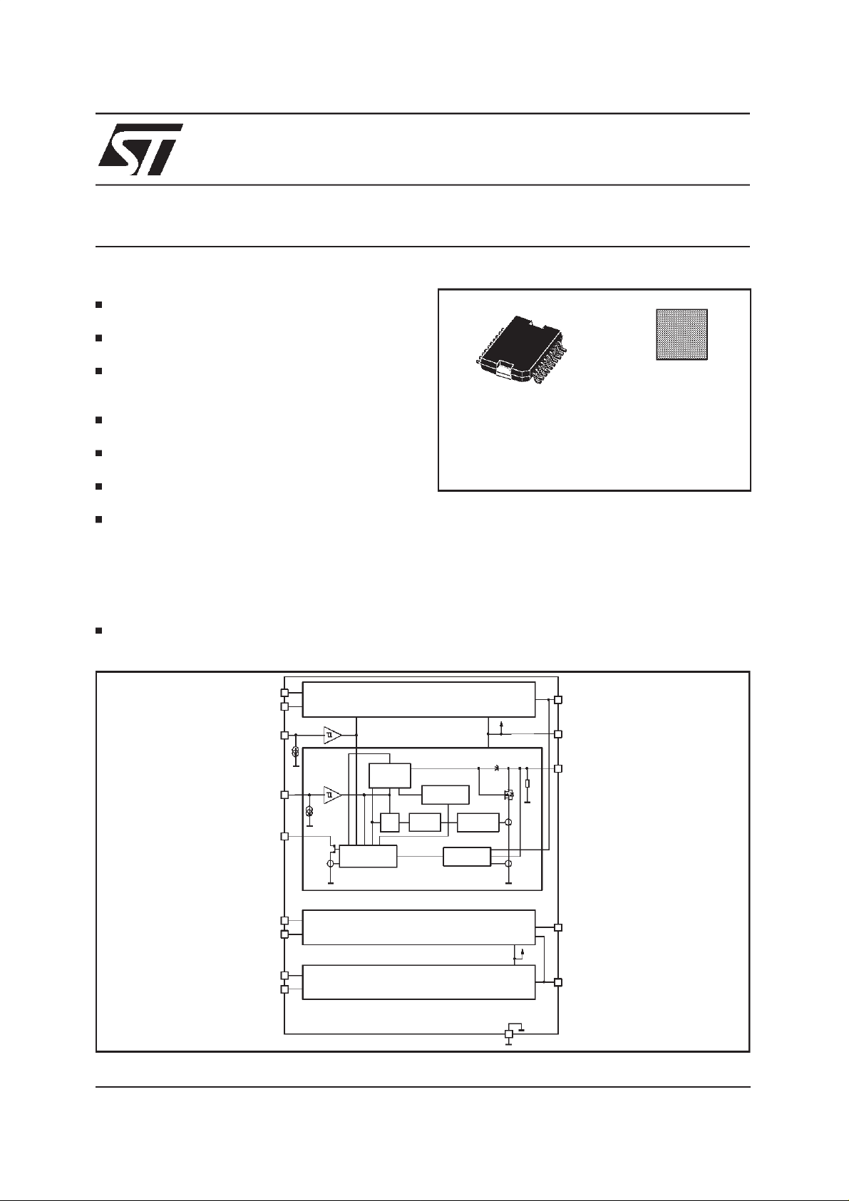
BLOCK DIAGRAM
TYPICALLY200mΩ AND 300mΩ
FB = 50V FOR FAST INDUC-
L9346
Power SO20
ORDERING NUMBERS: L9346PD (power SO20)
L9346DIE (chip)
- OVERLOAD DISABLE
- REVERSESUPPLYVOLTAGE
PROTECTEDVS UPTO-2V
- SELECTIVETHERMAL SHUTDOWN
DESCRIPTION
The L9346 is a monolithic integrated quad low
side driver realized in an advanced Multipow-
Chip
May 2000
IN1
D1
EN
IN4
D4
IN2
D2
IN3
D3
Diagnostic
Control
Output
Control
QS
Channel1
52V
Overtemp
Delay
R
Timer
Channel4
Channel2
Channel3
Overload
Openload
GND
OUT1
VS
OUT4
R
IO
OUT2
OUT3
1/13
Page 2
L9346
DESCRIPTION
(continued)
erBCD mixed technology. The device is intended
to drive valves in automotiveenvironment.
The inputsare µP compatible. Particularcare has
been taken to protect the device against failures,
to avoid electromagnetic interferences and to offer extensive realtime diagnostic.
ABSOLUTE MAXIMUM RATINGS
Symbol Parameter Conditions Value Unit
V
S
SP Supply Voltage Pulse (duration <200ms) -2 to 45 V
V
dV
S
dt
V
IN, EN
V
D
ODC DC Output Voltage -0.3 to 45 V
V
O1, 2 DC Output Current Out 1, 2 5 A
I
O3, 4 DC Output Current Out 3, 4 3 A
I
OR1, 2 Reverse Output Current -5 A
I
OR3, 4 Reverse Output Current -3 A
I
O1,2 Switch-off Energyfor Inductive Loads tEO = 250µs,
E
O3,4 T = 5ms 30 mJ
E
∆V
GND
T
jEO
j Juntion Temperature -40 to TjDIS °C
T
stg Storage Temperature -55 to 150 °C
T
jDIS Thermal DisableJunction Temp. Threshold 180 to 210 °C
T
DC Supply Voltage -2 to 32 V
Supply Voltage Slope 10 V/µs
Input Voltage I 10mA -2 to 16 V
Diagnostic DC Output Voltage I 50mA -0.3 to 16 V
1)
50 mJ
GND Potential Difference Tj= -40 to 150°C ±0.3 V
Juntion Temperature During Switch-off ∑t ≤ 30 min 175 °C
∑t ≤ 15 min 190 °C
The device is ESDprotected, testedaccording to MIL883Cwith ±2KV.
1)
:tEOis theclamping time (seefig.1)
Note
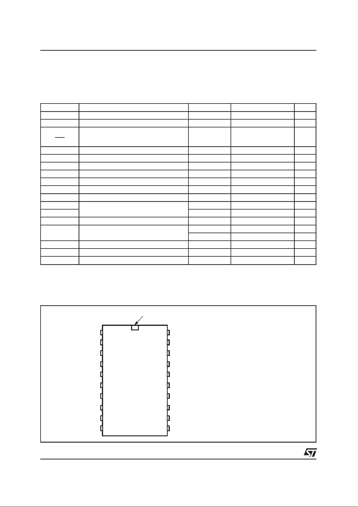
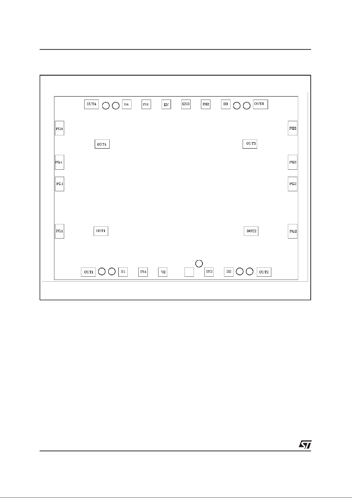
PIN CONNECTION
Heat sink connected to pins 1, 10, 11, 2 0
PGND
OUT1
D1
IN4
VS
NC
IN3
D2
OUT2
PGND
PGND
OUT4
D4
IN1
EN
GND
IN2
D3
OUT3
PGND
2/13
Page 3
THERMAL DATA
Symbol Parameter Value Unit
R
th j-c
Thermal Resistance junction to case 3 K/W
PIN FUNCTIONS
N. Name Function
1 GND Power Grounded
2 Out 1 Output 1 (5A)
3 D1 Diagnostic 1
4 IN 4 Input 4
5 VS Supply Voltage
6 NC Not Connected
7 IN 3 Input 3
8 D2 Diagnostic 2
9 Out 2 Output 2 (5A)
10 GND Power Ground
11 GND Power Ground
12 Out 3 Output 3 (3A)
13 D3 Diagnostic 3
14 IN 2 Input 2
15 GND Signal Ground
16 EN Common Enable
17 IN 1 Input 1
18 D4 Diagnostic 4
19 Out 4 Output 4 (3A)
20 GND Power Ground
L9346
Figure 1: tEO ClampingTime
V
O1 - 4
V
OC L
V
S
t
t
EO
T
3/13
Page 4
L9346
Figure 2: Pad Position
(Chipsize 4.95x 3.88)
ESD
4/13
Page 5

L9346
Pad Coordinates
Pad Nr. Pad Name Size in (µm) Description
1
2
3
4
5
6
7
8
9
10
11
12
13
14
15
16
17
18
19
20
21
22
23
24
25
26
27
(Referencepoint X = 0, Y = 0: Centerof die)
Pat opening center position
PG3
PG3
PG2
PG2
OUT2
OUT2
D2
IN3
VS
IN4
D1
OUT1
OUT1
PG1
PG1
PG4
PG4
OUT4
OUT4
D4
IN1
EN
GND
IN2
D3
OUT3
OUT3
Test pad Size X Y
Gate 2
VTERM2
IOLRED
ESD
VTERM1
GATE1
GATE4
VTERM4
VTERM3
GATE3
178 x 280
178 x 280
178 x 280
178 x 280
280 x 178
280 x 178
178 x 178
178 x 178
178 x 178
178 x 178
178 x 178
280 x 178
280 x 178
178 x 178
178 x 178
178 x 178
178 x 178
280 x 178
280 x 178
178 x 178
178 x 178
178 x 178
178 x 178
178 x 178
178 x 178
280 x 178
280 x 178
d = 102
d = 102
d = 102
178 x 178
d = 102
d = 102
d = 102
d = 102
d = 102
d = 102
Power Ground 3
Power Ground 3
Power Ground 2
Power Ground 2
Output 2 5A
Output 2 5A
Diagnostic 2
Input 3
Supply Voltage
Input 4
Diagnostic 1
Output 1 5A
Output 1 5A
Power Ground 1
Power Ground 1
Power Ground 4
Power Ground 4
Output 4 3A
Output 4 3A
Diagnostic 4
Input 1
Common Enable
Signal Ground
Input 2
Diagnostic 3
Output 3 3A
Output 3 3A
Coordinates in (µm)
XY
2286.5
2286.5
2286.5
2286.5
1472.5
1722.5
1036
648
-260
-648
-1036
-1722.5
-1472.5
-2286
-2286
-2286
-2286
-1448
-1656
-970
-582
-194
194
582
970
1656.5
1448.5
1447
1260
449.5
260
-1260
-1447
-1381
-1194.5
1194.5
1381
1175
506
98
-842
-844
-1644
-1644
-1644
-1644
-1644
-1644
-1644
-844
-842
98
506
1175
865
1644
1644
1644
1644
1644
1644
1644
1644
865
-1612
-1600
-1455.5
-1644
-1600
-1612
1600
1600
1600
1600
5/13
Page 6

L9346
ELECTRICALCHARACTERISTICS (Operating Range)
Theelectricalcharacteristicsarevalidwithinthe belowdefinedoperatingrange,unlessotherwise specified.)
Symbol Parameter Test Condition Min. Typ. Max. Unit
S Board Supply Voltage 4.5 12 32 V
V
T
j1 Junction Temperature -40 150 °C
T
j2 Junction Temperature Σt ≤ 15min
NOTE:
2)
Parameters guaranteed by correlation
2)
over life time 150 TjDIS °C
ELECTRICAL CHARACTERISTICS
S = 4.5 to 32V; -40°C ≤
(V
Τj1 ≤ 150°C<Tj2 ≤ ΤjDIS, unless other-
wise specified.)
Symbol Parameter Test Condition
Value T
j1
Min. Typ. Max. Min. Max.
Value T
j2
Supply
IVS OFF DC Supply Current Off EN = 1.0V 5 10 mA
I
VS ON
DC Supply Current On VS≤ 14V; VIN,VEN=2V 8 mA
DiagnosticOutputsD 1 - D 4
VDL Diagnostic Output Low
Voltage
I
DLE
Diagnostic Output
Leakage Current
ID ≤ 3mA 0.65 1.0 1.5 V
VD= 14V
3)
0.1 2 20 µA
OutputsOut 1 - Out 4
VOUV 1-4 Open Load Voltage
Threshold
V
OUV hys 1-4
∆V
OUV1-4,
2-3, 4-1, 3-2
V
OUV hys1-4,
2-3, 4-1, 3-2
I
OUC 1,2, 3,4 Open Load Current
Hysteresis 0.003 x
Open Load Difference
Voltage Threshold
Open Load Hysteresis 40 mV
Threshold
I
OOC 1, 2 Over Load Current
OOC 3, 4 3 6 2.4 A
I
V
OCL
Threshold
Output Voltage During
Clamping
S
ON,OFF Output (fall,rise) slew
rate
R
IO Internal Output Pull
Down Resistor
R
DSON 1, 2
R
DSON 3, 4
NOTE:
2)
Parameters guaranteed by correlation
3)
The diagnosticoutput is short circuit protected upto VD =16V
4)
VS= 9to 16V
Output On Resistance Tj=25°C
VIN =1V 0.525 x
VIN1,4/2,3 = 1V,
4.5V ≤ VO
4.5V ≤ V
VO
c = output voltage of
c
≤ 16V,
S
≤ 16V,
VO
1.0V
0.55 x
V
S
C -
VOC -
1.25V
0.575 x
V
S
V
S
VOC -
V
1.5V
S
0.5 x VS 0.65 x
V
VOC -
0.8V
VOC -
1.7V
other channel
VEN =VIN = 2V;
V
= 6.5 to 16V
S
VS > 6.5V;
V
OUT = 32V
I
≥ 200mA 45 52 60 V
OCL
4)
IOUC ≤ IO ≤ IOOC 400 1500 2850 200 3500 V/ms
160 320 480 580 mA
510 4 A
VEN =1V 10 20 40 50 KΩ
200 300
T
j= 150°C
V
S > 9.5V, IO1,2 =2A
Tj=25°C
T
= 150°C; I
j
O3,4
= 1.3A
300 450
500
750
Unit
V
S
V
V
mΩ
mΩ
6/13
Page 7

ELECTRICALCHARACTERISTICS (continued)
L9346
Symbol Parameter Test Condition
Value T
j1
Min. Typ. Max. Min. Max.
Value T
InputsIN1-4,EN
V
IN,EN L
V
IN,EN H Logic Input/EnableHigh
V
EN,IN hys Logic Input Hysteresis 0.2 0.4 0.8 V
I
IN Input Sink Current VIN = 2 to12V
I
EN
Timing
tDON Output Delay ON Time
t
D OFF Output Delay OFF Time
t
DH-L, Diag
t
D IOU Diagnostic Open Load
t
DOL
t
DENON Enable ON Time
t
D ENOFF
NOTE:
5)
Open pins (EN, IN) are detected as low
6)
VS= 9to 16V ∧ I
Logic Input/Enable Low
-0.3 1 0.8 V
Voltage
IN, EN 2.0 16 V
Voltage
5)
10 30 60 240 µA
Enable Sink Current 10 20 40 240 µA
6)
Fig. 7 4 25 µs
6)
Fig. 7 5 15 30 µs
Diag. Delay Output
6)
Fig. 6 8 65 90 µs
OFF Time
Delay Time
Diagnostic Overload
Delay Switch-OFF Time
Enable OFF Time
OUC
≤ IO≤ I
OOC
VS = 9 to 16V, Fig8
I
O ≤ IOUC
VS= 9 to 16V, Fig 8
I
O >IOOC
6)
Fig. 7 4 25 µs
6)
Fig. 7 4 25 µs
50 160 300 µs
850 µs
DIAGNOSTICTABLE
j2
Unit
CONDITIONS EN IN OUT DIAG.
Normal Function L X off L
H L off L
7)
7)
GND short V
Load bypass ∆V
Open Load I
jtyp ≥ 190°C Overtemperature
T
O1,2,3,4typ < 320mA H H on
Over Load I
HHon
Otyp < 0.55VS L X off H
O1-4/2-3 ≥ 1.25V H L off H
Omin 1,3 >5A
I
>3A
Omin 2,4
8)
X X off L
H H off L
Reset and Overtemperature Latch X DC don’t care DC don’t care
NOTE:
7)
For VS= 4.5to 6.5V,IO≤ 2A, thediag. table isvalid
8)
If one diag. status shows the overtemperature,recognition, in parallelthis output will be switched OFFinternally.
Thecorresponding channelshouldbe switchedOFFadditionally by itsinputsignal, otherwise the overload latch willbe setaftert
This behaviouris related tothe overdrop sensing which is used asover load recognition.
The overtemperature is latched (DIAG = L) until the level ofthe IN signalchanges to low.
H
L
ispassed.
DOL
7/13
Page 8

L9346
CIRCUIT DESCRIPTION
The L9346 is a quad low side driver for inductive
loads like valves in automotive environment. The
internal pull down current sources at the ENABLE and INPUT pins assure in case of open input conditionsthat the device is switched off. An
output voltage slope limitation for du/dt is implemented to reduce the EMI. An integrated active
flyback voltage limitation clamps the output voltage during the flyback phase to 50 V.
Each driver is protected against short circuit at
OUT < 32V and thermal overload. In short circuit
V
condition the output will be disabled after a short
DOL
delay time t
. The thermal disable for TJ >
180°C of the output will be reseted if the junction
temperaturedecreasesabout 20°Cbelow the disable threshold temperature.
Theov er temperatureinformationisstoreduntilIN=L.
For the real time error diagnosis the voltage and
the current of the outputs are compared with internal fixed values V
conditions to recognize open load (R
R
L >38Ω) in OFFand ON conditions.
Also the output voltages V
OUV for OFF and IOUC for ON
L ≥ 20 KΩ,
O1
- 4 are compared to
each other output in OFF condition with a fixed
Figure 3. Diagnostic OverloadDelay Time
offset of ∆V
suppress the ∆V
OUV to recognize load bypasses. To
OUV diagnoses duringthe flyback
phases of thecomparedoutput, the∆VOUVdiagnostic includesa latch function.
Reaching the flyback clamping voltage V
OCL the
diagnostic signalisresetedby a latch. To activate
again this kind of diagnostic a low signal at the
correspondent INPUT or the ENABLE pin must
be applied (see also Fig.3). The outputs 1 and 4
are compared for ∆V
OUV and also outputs 2 and 3
are compared.
The diagnosticoutput level in connectionwith dif-
ferent ENABLE and INPUT conditions allows to
recognize differentfailstates,like overtemp,short
SS, short to GND, bypass to GND and dis-
to V
connectedload (see diagnostictable).
The diagnostic output is protected against short
circuit. Exceeding the over load current threshold
OOC
, the output current will be limited internally
I
during the diagnostic overload delay switch-off
time t
DOL.
The device complies the ISO pulses imposed to
the supply voltage of the valves without any failures of the functionality.
I
I
V
OOL
OUC
IN
5V
t
I
O
5A
3A
t
DOL
V
D
5V
t
8/13
t
Page 9

Figure 4. OUTPUT SLOPE(Resistive load for testing)
V
IN
5V
V
(EN)H
V
(EN)L
V
OUT
0.85VS
V
OUV
0.15VS
VS
t
DON
t
DENO N
S
ON
t
D OFF
t
DENO FF
L9346
t
S
OFF
0.85VS
t
V
DIAG
V
D
0.5V
D
Figure 5. TIMING(tDENON,tDON,tDENOFF,tDOFF)
EN, IN
V
ON
0.85 x V
t
DENON
OUT
, DON
t
t
D
H-L
Diag
0.15 xV
OUT
tt
DEN OFF
, DO FF
t
9/13
Page 10

L9346
Figure 6. TIMING (tDOL,tDIOU)
IN
V
ON
I
OOC
I
OUC
V
D
t
DIOU
Open load current
Figure 7. BLOCKDIAGRAM- Open LoadVoltage Detection
t
DOL
V
Batt.
L1 (L2) L4 (L3)
OUT1 OUT4
(OU T2) (OU T3)
IN
1
VS
55%
Enable
R
R
IO
IO
+
-
+
-
IN
4
&&
R
S
Latch
Q
Latch
S
Q
R
10/13
&&
VO
UV1
VO
UV4
Page 11

Figure 8. LogicDiagram
V
EN
V
IN
VO
u
IO
o
IO
u
V
D
open load current
normal
operation
ON
open l oad
current
latched over.
load diagnostic
L9346
nor mal
ope rati on
latch reset
ON
open load current
op en load v oltag e
normal
operation
OFF
open load
voltage
Figure 9. ApplicationCircuit Diagram
+5V
Controller
VCC
I/O
I/O
I/O
I/O
I/O
µ P
I/O
I/O
I/O
I/O
IN1
D1
EN
Output
Control
IN4
+5V
D4
+5V
Diagnostic
Control
IN2
D2
+5V
IN3
D3
R
QS
Cha nne l 1
Delay
Timer
Cha nne l 4
Cha nne l 2
Cha nne l 3
Overtemp
Overload
Op enloa d
52V
Z
VALVE
OUT1
VS
+45V
OUT4
R
IO
Z
Z
VALVE
VALVE
V
Batt
KL15
KL30
OUT2
Z
VALVE
OUT3
GND
GND
11/13
Page 12

L9346
DIM.
MIN. TYP. MAX. MIN. TYP. MAX.
mm inch
A 3.6 0.142
a1 0.1 0.3 0.004
a2 3.3
0.012
0.130
a3 0 0.1 0.000 0.004
b 0.4 0.53 0.016 0.021
c 0.23 0.32 0.009 0.013
D (1) 15.8 16 0.622 0.630
D1 9.4 9.8 0.370 0.386
E 13.9 14.5 0.547 0.570
e 1.27 0.050
e3 11.43 0.450
E1 (1) 10.9 11.1 0.429 0.437
E2 2.9
0.114
E3 5.8 6.2 0.228 0.244
G 0 0.1 0.000 0.004
H 15.5 15.9 0.610 0.626
h 1.1
0.043
L 0.8 1.1 0.031 0.043
N10°(max.)
S
8°(max.)
T 10 0.394
(1) ”Dand F”do notinclude moldflashor protrusions.
- Moldflashor protrusions shall notexceed0.15 mm(0.006”).
- Criticaldimensions: ”E”, ”G” and ”a3”
OUTLINE AND
MECHANICAL DATA
JEDEC MO-166
PowerSO20
E2
hx
45
DETAIL B
BOTTOM VIEW
R
Gage Plane
c
a1
E
L
DETAIL A
slug
-C-
SEATING PLANE
GC
(COPLANARITY)
E3
lead
a3
DETAIL B
0.35
S
D1
NN
a2
A
b
DETAIL A
e3
H
D
T
1
e
1120
E1
10
PSO20MEC
12/13
Page 13

L9346
Information furnished is believedto be accurate and reliable. However,STMicroelectronics assumes no responsibility for the consequences
of use of such information nor for any infringement of patents or other rights of third parties which may result from its use. No license is
granted by implication or otherwise under any patent or patent rights of STMicroelectronics. Specification mentioned in this publication are
subject to change withoutnotice. This publication supersedes and replaces all information previously supplied. STMicroelectronics products
are not authorizedfor use as critical components in lifesupport devices orsystems without express writtenapproval of STMicroelectronics.
The ST logois a registeredtrademark of STMicroelectronics
2000 STMicroelectronics – Printedin Italy – All Rights Reserved
STMicroelectronics GROUP OFCOMPANIES
Australia - Brazil - China- Finland - France- Germany -HongKong - India- Italy - Japan - Malaysia - Malta- Morocco -
Singapore - Spain - Sweden - Switzerland - UnitedKingdom - U.S.A.
http://www.st.com
13/13
 Loading...