

Page 1
■
WIDE OPERATING SUPPLY VOLTAGE
RANGE FROM 4.5V UP TO 32V FOR
TRANSIENT 45V
■
VERY LOW STANDBY QUIESCENT
CURRENT < 2µA
■ INPUT TO OUTPUT SIGNAL TRANSFER
FUNCTION PROGRAMMABLE
■
HIGH SIGNAL RANGE FROM -0.3V UP TO
32V FOR ALL INPUTS
■
TTL AND CMOS COMPATIBLE INPUTS
■ DEFINED OUTPUT OFF STATE FOR OPEN
INPUTS
■
FOUR OPEN DRAIN DMOS OUTPUTS, WITH
R
■ OUTPUT CURRENT LIMITATION
■ CONTROLLED OUTPUT SLOPE FOR LOW EMI
■ OVERTEMPERATURE PROTECTION FOR
= 1.5ΩFOR VS>6VAT25°C
DSon
EACH CHANNEL
■
INTEGRATED OUTPUT CLAMPING FOR FAST
INDUCTIVE RECIRCULATION V
FB
>45V
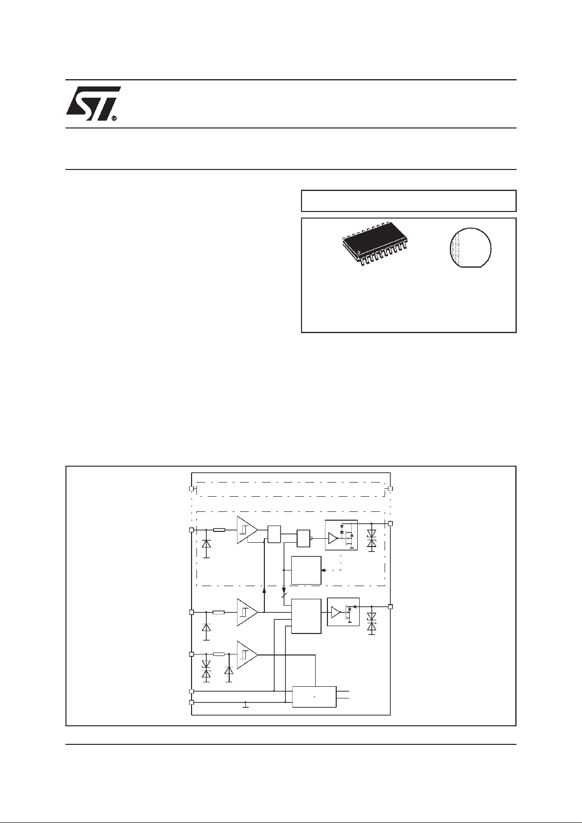
L9339
QUAD LOW SIDE DRIVER
MULTIPOWERBCD TECHNOLOGY
SO20 & SO20(12+4+4) BARE DIE
ORDERING NUMBER:
L9339MD (SO20 12+4+4)
L9339 (SO20)
L9339DIE1 (BARE DIE)
■
STATUS MONITORING FOR
- OVERTEMPERATURE
- DISCONNECTED GROUND OR SUPPLY
VOLTAGE
DESCRIPTION
The L9339 is a monolithic integrated quad low side
driver. It is intended to drive lines, lamps or relais in
automotive or industrial applications.
BLOCK DIAGRAM
December 1999
IN 4
IN 1
PRG
GND
EN
VS
CHANNEL4
CHANNEL1
=
THERMAL
SHUTDOWN
4
DIAGNO ST IC
LOGIC
REFERENCE
OUT4
OUT1
&
DIAG
Vint
Vlogic
1/9
Page 2
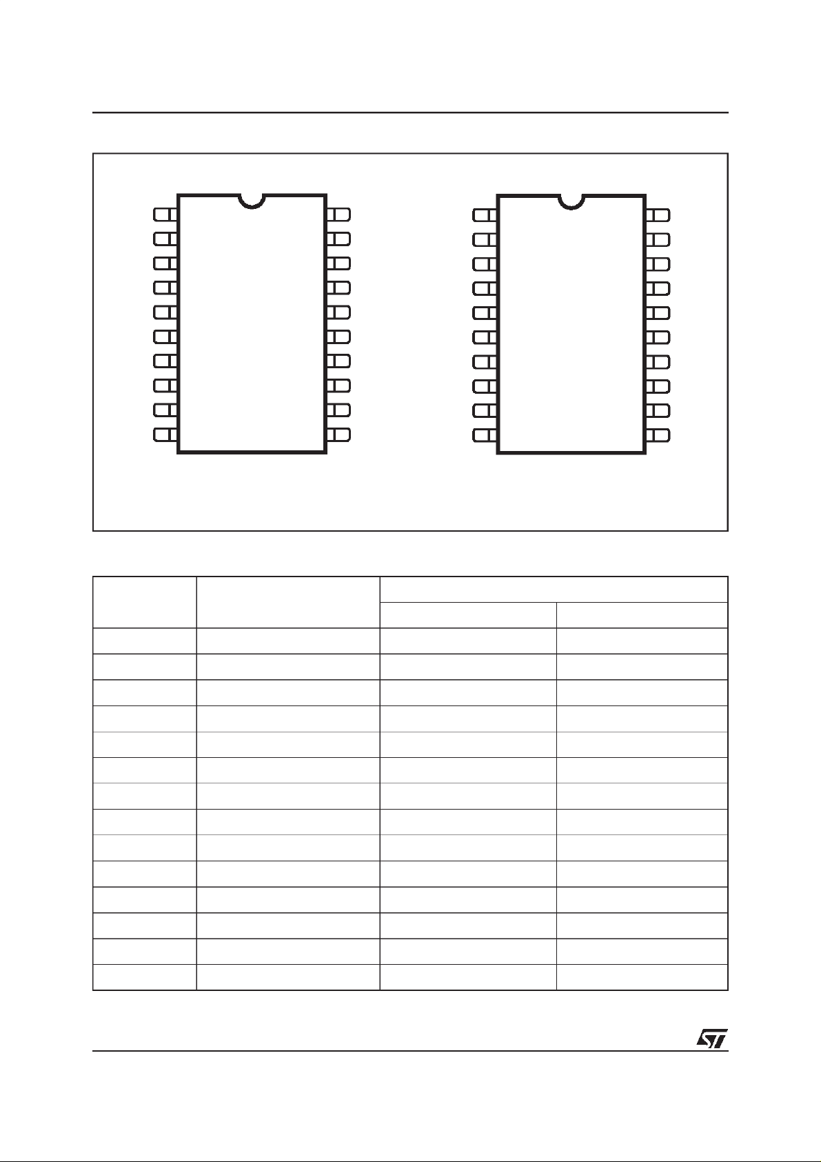
L9339
PIN CONNECTION (Top view)
NC
VS
NC
IN3
IN4
EN
OUT4
OUT3
GND NC
NC NC
2
3
4
5
6
7
8
9
10
SO20
20
19
18
17
16
15
14
13
12
11
SO20 SO20 (12+4+4)
PIN FUNCTION
Pin Name Description
NC1
DIAG
NC
IN2
IN1
PRG
OUT1
OUT2
IN1
IN2
DIAG
GND
GND
GND
GND
VS
IN3 OUT4
IN4 EN
SO 20 SO 20 (SO 12+4+4)
2
3
4
5
6
7
8
9
10
SO20 (12+4+4)
Package
20
19
18
17
16
15
14
13
12
11
PRG1
OUT1
OUT2
GND
GND
GND
GND
OUT3
VS Supply Voltage 2 8
GND Ground 9 4, 5, 6,7, 14, 15, 16, 17
EN Enable 6 11
PRG Programing 15 20
DIAG Diagnostic 19 3
IN 1 Input 1 16 1
IN 2 Input 2 17 2
IN 3 Input 3 4 9
IN 4 Input 4 5 10
OUT 1 OUTPUT 1 14 19
OUT 2 OUTPUT 2 13 18
OUT 3 OUTPUT 3 8 13
OUT4 OUTPUT4 7 12
NC Not Connected 1,3,10,11,12,18,20 -
2/9
Page 3
L9339
ABSOLUTEMAXIMUM RATINGS
(no damage or latch)
Symbol Parameter Value Unit
V
S
Supply voltage DC
Supply voltage Pulse (T < 400ms)
/dt Supply voltage transient -10 ... +10 V/µs
dV
S
V
IN,VPRG
Input, Programming DC voltage
Input, Programming Pulse (T <400ms)
I
IN
V
EN
Negative input current -10 mA
Enable voltage DC
Enable voltage Pulse (T <400ms)
V
I
OUT
OUT
Output voltage
Negative output current
Positive output current
V
DIAG
Diagnostic output voltage DC
Diagnostic output voltage Pulse (T < 400ms)
Notes: 1. In flyback phase the output voltage can reach 60V.
ESD according toMIL 883C; tested at 2KV;corresponds to maximum energy dissipation 0.2mJ.
-0.3 ... 32
-0.3 ... 45
-0.3 ... 32
-0.3 ... 45
-24 ... 32
-24 ... 45
-0.3 ... 45
1)
-1
internal limited
-0.3 ... 32
-0.3 ... 45
V
V
V
V
V
V
V
A
V
V
THERMAL DATA
Symbol Parameter Min. Typ. Max. Unit.
T
JSDon
T
JSDoff
SO 12+4+4
R
th j-pin
R
th j-amb
SO 20
R
th j-amb
2. With 6cm2on board heat sink area.
3. Mounted onSMPCB2 board
Temperature shutdown switch-on-threshold 160 200 °C
Temperature shutdown switch-off-threshold 140 180 °C
Thermal resistance junction to pins 15 °C/W
Thermal resistance junction to ambient
Thermal resistance junction to ambient
2)
3)
50 °C/W
97 °C/W
3/9
Page 4

L9339
ELECTRICAL CHARACTERISTCS
The electrical characteristics are valid within the below defined Operating Conditions, unless otherwise specified. The function is guaranteed by design until T
Supply voltage 4.5 V to 32 V
V
S
Junction temperature -40 °Cto150°C
T
j
Ambient Temperature -40 °Cto125°C
T
amb
Note: Ambient test temperature = -40 °C to 125 °C
Symbol Parameter Test Condition Min. Typ. Max. Unit
SUPPLY:
switch-on-threshold.
JSDon
I
Quiescent current -0.3V < VEN< 0.5V; VS=14V;
Q
Inputs, IN1 - IN4; Programming, PRG:
V
V
INhigh
INlow
Input voltage LOW -0.3 2.0 V
Input voltage HIGH 2.8 32 V
Input current VIN= 0 ...32V -15 25 µA
I
IN
Enable EN:
V
ENlow
V
ENhigh
R
I
Input voltage LOW -24 1 V
Input voltage HIGH 3.2 V
Input impedance -24 V < VIN< 2.5 V 10 k
EN
Input current 2.5 V < VIN< 32V 20 80 µA
EN
Outputs OUT1- OUT4
R
DSon
I
OLeak
Output ON-resistor VS>6V,IO= 0.3A 1.7 3.8
Leakage current
-0.3V < V
< 125 °C
T
a
< 150 °C
T
a
V
> 3.2V; VS< 14V 1.5 2 mA
EN
< 0.5V; VS=14V;
EN
<2 10 µA
50 µA
S
V
Ω
Ω
=14V;Ta< 125 °C<15µA
V
O=VS
V
OClamp
I
OSC
C
Output voltage during clamping time < 200µs
Short-circuit current 4.5V < VS< 6V 0.3 1 A
internal output capacities VO> 4.5V 100 pF
O
Diagnostic Output DIAG
V
Dlow
I
Dmax
Output voltage LOW IDL< 0.6mA 1.3 V
Max. output current internal current limitation
4/9
=VS=14V;Ta< 150 °C25µA
V
O
45 52 60 V
10 mA< I
> 6V 0.4 0.7 1 A
V
S
<0.3A
O
1515mA
V
=14V
D
Page 5

L9339
ELECTRICAL CHARACTERISTICS
(Continued)
Symbol Parameter Test Condition Min. Typ. Max. Unit
I
DLeak
TIMING CHARCTERISTICS
t
d,on
t
d,off
t
t
d,DIAG
S
Note : All parameters are measured at T
Leakage current VD=VS=14V;Ta<125°C<0.11µA
=VS=14V;Ta<150°C5µA
V
D
4)
On delay time VS=14V,C
10mA < I
Off delay time 3 4.5 µs
Enable settling time 10 µs
set
ext
< 200mA
O
= 0pF
2 3.5 µs
ON or OFF Diagnostic delay time 10 µs
Output voltage slopes 2.5 9 16 V/µs
out
= 125°C.
4. See also Fig.3 Timing Characteristics
amb
Figure 1.
V
EN
V
INhig h
V
IN lo w
active
V
PRG
Non-InvertingMode Inverting Mode
V
INhig h
V
IN lo w
V
IN
V
INhig h
V
IN lo w
V
OUT
V
S
1/2 V
S
t
set
t
d,off
t
d,on
5. Output voltage slope not controlled for enable low!
t
t
t
5)
t
t
d,off
t
d,on
t
d,off
t
d,on
t
set
5/9
Page 6

L9339
FUNCTIONAL DESCRIPTION
The L9339 isa quad low side driver for lines, lamps or inductiveloads in automotive and industrial applications.
The logic input levels are TTL and CMOS compatible. This allows the device to be driven directly by a micro-
controller. For the noise immunity, all input thresholds has a hysteresis of typ. 100mV. At each input (IN and
PRG) voltages from -0.3V to 32V can be applied, EN can withstand voltages from -25V to 32V. The device is
activated with a’high’ signal on ENable. ENable ’low’ switches the device intothe sleep mode.In this mode the
quiescent current is less than 10µA. A high signal on PRoGramming input changes the signal transfer polarity
from noninverting into the inverting mode. This pin can be connected to V
PRG and EN pin is low, if these pins are not connected. This forced condition leads to a mode change if the
PRG pin was high before the interruption. Independent of the PRoGramming input, the OUTput switches off, if
the signal INput pin is not connected.
Each output driver hasa current limitation of min 0.4A anda independent thermal shut-down. The thermal shutdown deactivates that output, which exceeds temperature switch off level. When the junction temperature decreases 20K below this temperature threshold the output will be activated again (hysteresis of the thermal shutdown function). The slew rate of the output voltage is limited to max. 14V/µs, to reduce the electromagnetic
radiation of theloads and its wiring. For inductive loads aoutput voltage clamp of typicaly 52Vis implemented.
The DIAGnostic is an open drain output with an additional series diode. The logic status depends on the PRoGramming pin. If the PRG pin is ’low’ the DIAG output becomes low, if the device works correctly. At thermal
shut-down of one channel the DIAGnostic output becomes high. If the PRG pin is ’high’ this output is switched
off at normal function and switched on at overtemperature.
or GND. The forced status of the
S
Diagnostic Table
Pins EN PRG IN OUT DIAG
Correct function H L L L (on) L (on)
H L H H (off) L (on)
H H L H (off) H (off)
H H H L (on) H (off)
L X X H (off) H (off)
Overtemperature
or supply voltage H L X H (off) * H (off)
Overtemperature H H X H(off) * L(on)
X = not relevant * selective for each channel at overtemperature
6/9
Page 7

Figure 2. Application for Inverting Transfer Polarity
BO AR D VOLT AG E 14 V
VCC = 5V
10µF
L9339
VCC
MICROCONTROLLER
GND
IN T
D0
D1
D2
D3
AdressdecoderA0:8
8
PR G
EN
IN 1
IN 2
IN 3
IN 4
VS
DIAG
U717
L9339
OUT 1
OUT 2
OUT 3
OUT 4
GND
Figure 3.Application for Non Inverting Transfer Polarity
BO ARD VO LTAG E 14 V
VC C = 5 V
2W 12mH
50 kHz
M
10µH
250 mA
240Ω
50pF
VC C = 5V
VCC
IN
GND
10µF
VCC
MICROCONTROLLER
GND
IN T
D0
D1
D2
D3
AdressdecoderA0:8
8
PR G
EN
IN 1
IN 2
IN 3
IN 4
VS
DIAG
L9339
U717
OUT 1
OUT 2
OUT 3
OUT 4
GND
2W 12mH
50 kHz
Note: We recommend to use the device fordriving inductive loads with flyback energy EFB< 2mJ.
M
10µH
250 mA
240
50pF
VCC = 5V
Ω
VC C
IN
GND
7/9
Page 8

L9339
DIM.
MIN. TYP. MAX. MIN. TYP. MAX.
A 2.35 2.65 0.093 0.104
A1 0.1 0.3 0.004 0.012
B 0.33 0.51 0.013 0.020
C 0.23 0.32 0.009
D 12.6 13 0.496 0.512
E 7.4 7.6 0.291 0.299
e 1.27 0.050
H 10 10.65 0.394 0.419
h 0.25 0.75 0.010 0.030
L 0.4 1.27 0.016 0.050
K0°(min.)8°(max.)
mm inch
0.013
OUTLINE AND
MECHANICAL DATA
SO20 & SO20(12+4+4)
SO20
B
e
D
1120
110
L
hx45°
A
K
A1 C
H
E
SO20MEC
8/9
Page 9

L9339
Information furnished is believed to be accurate and reliable. However, STMicroelectronics assumes noresponsibility for the consequences
of use of suchinformationnor for anyinfringement of patents orother rights of third partieswhichmay result fromits use.No licenseis granted
by implication or otherwise under any patent or patent rights of STMicroelectronics. Specifications mentioned in this publication are subject
to change withoutnotice. This publication supersedes and replaces all information previously supplied. STMicroelectronics products are not
authorized for use as critical components in life support devices or systems without express written approval of STMicroelectronics.
The ST logo is a registered trademark of STMicroelectronics
1999 STMicroelectronics - All Rights Reserved
Australia - Brazil - China - Finland - France - Germany - Hong Kong - India -Italy - Japan - Malaysia -Malta - Morocco - Singapore - Spain
STMicroelectronics GROUP OFCOMPANIES
- Sweden - Switzerland - UnitedKingdom - U.S.A.
http://www.st.com
9/9
 Loading...