

Page 1
WIDE INPUT VOLTAGE RANGE FROM -24V
UP TO +45V
WIDE OPERATING SUPPLY VOLTAGE
RANGEFROM 4.5VUP TO32V
REVERSEBIASINGPROTECTED(V
= -24V)
S
VERY LOW STANDBY QUIESCENT CURRENT < 2µA
PROGRAMMABLE SIGNAL TRANSFER POLARITY
TTL AND CMOS COMPATIBLEINPUTS
DEFINED OUTPUT OFF STATE OFF FOR
OPEN INPUTS
FOUR OPEN DRAIN DMOS OUTPUTS, WITH
= 1.5Ωat 25°Cand VS>6V
R
DSon
OUTPUTCURRENT LIMITATION
CONTROLLEDOUTPUTSLOPEFORLOWEMI
OVERTEMPERATURESHUT-DOWN
INTEGRATED OUTPUT CLAMPING FOR
FASTINDUCTIVERECIRCULATIONV
FB
>45V
STATUSMONITORINGFOR
- OVERTEMPERATURE
- DISCONNECTED GROUND OR SUPPLY
L9338
QUAD LOW SIDE DRIVER
ORDERING NUMBERS: L9338D (SO20)
L9338MD (SO20 (12+4+4))
VOLTAGE
ESD: ALL PINS ARE GUARANTEED TILL2kV
HUMANBODYMODEL
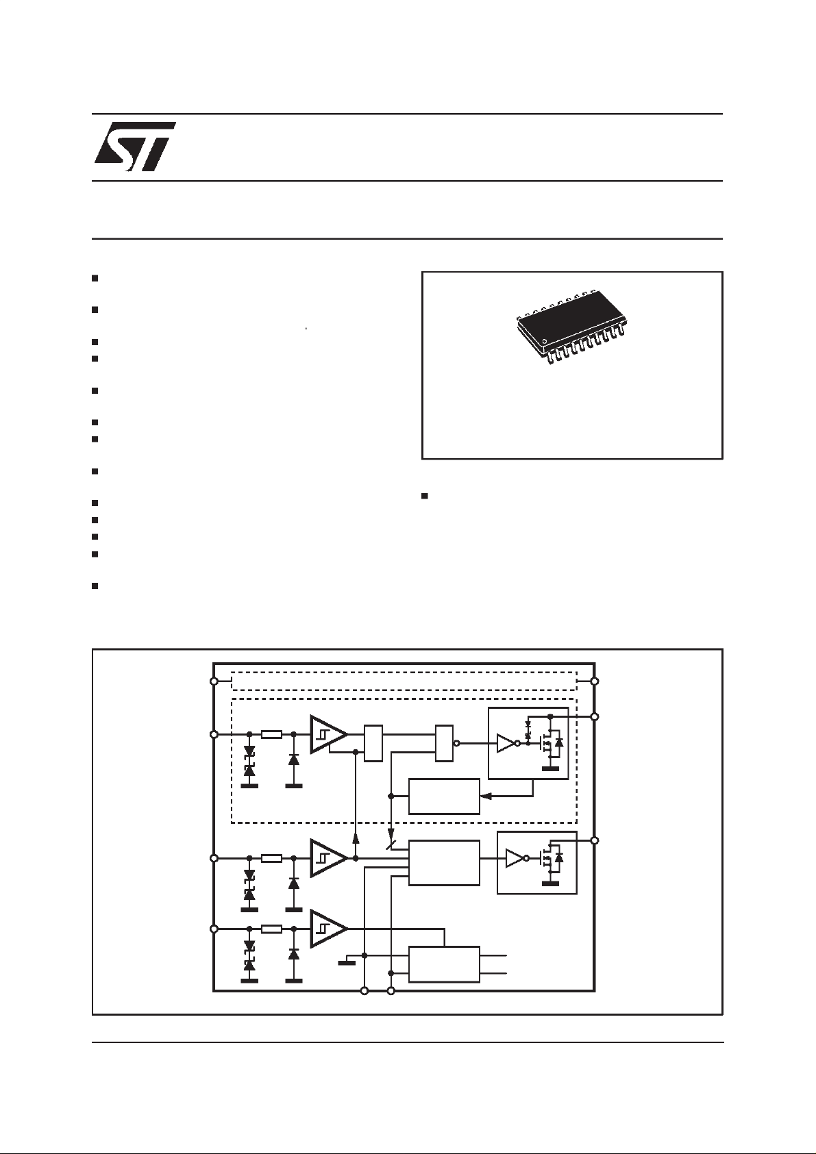
DESCRIPTION
The L9338 is a monolithic integrated quad low
side driver realized in advanced Multipower-BCD
technology. It is intended to drive lines, lamps or
relais in automotiveor industrialapplications.
BLOCK DIAGRAM
IN1
PRG
EN
March 2000
CHANNEL 4IN4
CHANNEL 1
=&
THERMAL
SHUTDOWN
4
DIAGNOSTIC
LOGIC
Vint
REFERENCE
VSGND
Vlogic
OUT4
OUT1
DIAG
D95AT149
1/8
Page 2
L9338
ABSOLUTE MAXIMUM RATINGS
(nodamage or latch)
Symbol Parameter Value Unit
V
S
Supply voltage -24 to 45 V
Pin voltages
V
IN
V
OUT
V
DIAG
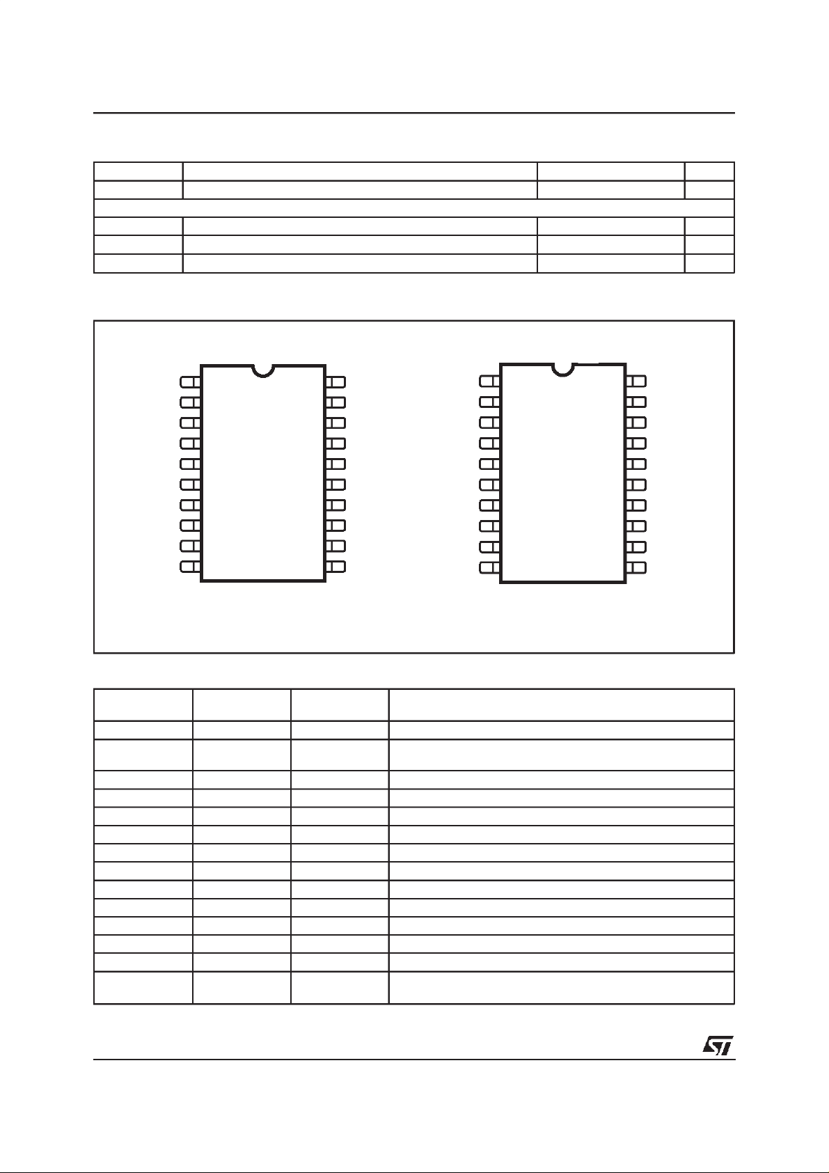
PIN CONNECTIONS
N.C.
N.C.
OUT4
OUT3
GND N.C.
N.C. N.C.
Input, enable, program -24 to 45 V
Output -0.3 to 45 V
Diagnostic output -0.3 to 45 V
(Top view)
20
19
18
17
16
15
14
13
12
11
VS
IN3
IN4
EN
2
3
4
5
6
7
8
9
10
D94AT120B
20
19
18
17
16
15
14
13
12
11
N.C.1
DIAG
N.C.
IN2
IN1
PRG
OUT1
OUT2
IN1
IN2
DIAG
GND
GND
GND
GND
VS
IN3 OUT4
IN4 EN
2
3
4
5
6
7
8
9
10
D94AT121A
PRG1
OUT1
OUT2
GND
GND
GND
GND
OUT3
PIN DESCRIPTION
SO20
N
o
2 8 VS SUPPLY VOLTAGE
9 4,5,6,7,14,
6 11 EN ENABLE
15 20 PRG PROGRAM
19 3 DIAG DIAGNOSTIC
16 1 IN1 INPUT 1
17 2 IN2 INPUT 2
4 9 IN3 INPUT 3
5 10 IN4 INPUT 4
14 19 OUT 1 OUTPUT 1
13 18 OUT 2 OUTPUT 2
8 13 OUT 3 OUTPUT 3
7 12 OUT 4 OUTPUT 4
3, 18, 1, 10, 11,
12, 20
SO20
SO 12+4+4
N
o
Pin Name Function
GND GROUND
15,16,17
– NC NOT CONNECTED
SO20 (12+4+4)
2/8
Page 3
L9338
THERMAL DATA
Symbol Parameter SO20 (2) SO(12+4+4) (1) Unit
R
th (j-pins)
R
th (j-amb)
T
jMon
(1) See SGS-THOMSON Microelectronics databook:”Thermal Management in Surface Mount Technology”
(2) See SGS-THOMSON Microelectronics databook:”Thermal characteristics of SO20”
OPERATING CONDITIONS (The electrical characteristics are valid within the below defined operating
ranges,unlessotherwisespecified.The functionwillbe guarantedby designuntilT
Symbol Parameter Value Unit
V
S
V
IN
V
EN
V
OUT,VD
T
j
Thermal resistance junction to pin – 14 (Typ.) °C/W
Thermal resistance junction to ambient mounted on
77 to 97 – °C/W
SMPCB2 board
Temperature-monitoring
Switch-off-level
Switch-on-level
160 to 190
140 to 170
jMON
°C
°C
switch-OFF-level.
Supply Voltage 4.5 to 32 V
Input pin voltage -24 to 45 V
Enable pin voltage -24 to 45 V
Output pin voltage -0.3 to 45 V
Junction temperature -40 to 150 °C
ELECTRICALCHARACTERISTICS
(Refer to the test circuit, unless otherwise specified.)
Symbol Parameter Test Condition Min. Typ. Max. Unit
I
Q
Quiescent current -0.3V ≤ VEN≤ 0.5V;
V
= 14V; Tj=85°C
S
EN = high; V
≤ 14V 1.5 2 mA
S
<2 10 µA
Inputs IN1 -IN4, PRG
V
V
INIlow
INhigh
I
IN
Input voltage LOW -24 2.0 V
Input voltage HIGH 2.8 45 V
Input current -24V ≤ Vi ≤ 10V -10 15 µA
Enable Input EN
V
V
ENhigh
R
ENlow
EN
I
EN
Input voltage LOW -24 1 V
Input voltage HIGH 3.2 VS V
Input impedance -24V < Vi< 2.5V 10 K
Input current 2.5V ≤ Vi ≤ 25V 20 50 µA
Outputs OUT1-OUT4
R
DSon
I
OLeak
V
OClamp
I
OSC
C
O
Output ON-resistor to ground VS≥ 6V, IO= 0.3A
T
=25°C
j
T
= 125°C
j
1.7 2.3
3.5
Leakage current VO=VS= 14V; Tj=85°C ≤15µA
Output voltage during clamping time < 200µs; 10mA ≤ Io≤ 0.3A 45 52 60 V
Short-circuit current 400 700 1200 mA
Internal output capacities V
4.5V 100 pF
≥
O
Diagnostic output DIAG
V
Dlow
I
Dmax
I
Dleak
Output voltage LOW IDL≤ 1mA 0.3 0.5 V
Max. Output current Internal current limitation 1 5 15 mA
Leakage current VS= 14V; TJ=85°C
0.1 1
≤
Ω
Ω
Ω
A
µ
3/8
Page 4

L9338
ELECTRICALCHARACTERISTICS
(Continued)
Symbol Parameter Test conditions Min. Typ. Max. Unit
Timing
t
d,on
t
d,off
t
set
t
d,DIAG
S
out
(see Fig. 1)
On delay time VS= 14V, C
Off delay time 3 4.5
10mA ≤ I
ext
≤ 200mA
O
= 0pF
2.5 3.5
Enable settling time 10 µs
On or Off diagnostic delay time 10 µs
Output slopes 2.5 9 16 V/µs
Figure 1
V
EN
V
INhigh
V
INlow
active
t
V
PRG
s
µ
s
µ
V
INhigh
V
INlow
V
V
INhigh
V
INlow
V
1/2V
IN
OUT
V
S
S
Non-Inverting Mode
t
set
t
d,offtd,on
No controlled output slope for enable low
t
d,off
Inverting Mode
t
d,on
t
d,off
t
d,on
D95AT150
t
t
t
t
set
4/8
Page 5

L9338
CIRCUIT DESCRIPTION
The L9838 is a quad low side driver for lines,
lamps orinductive loads in automotive and industrial applications.
All INputs are TTL or CMOS compatible. This allows the device to be driven directly by a microcontroller. For the noiseimmunity, all inputs have
a Schmitt-triggerwith a hysteresis of typ. 100mV.
Each input stage has an input voltage protection
from -24V to 45V. The device can be activated
with a ’high’ signal on ENable input. ENable ’low’
switches the device into the sleep mode. In this
mode the quiescent current is less than 10µA. A
high signal on PRoGramming input changes the
signal transfer polarity from noninverting into the
inverting mode. Normally this pin is connected to
or GND. These pins (PRG and EN) are inter-
V
S
nally fixed at low status by open input condition.
Independent of the PRoGramming input, the
OUTput switches off, if the signal INput pin is not
connected.
Each output driver has a current limitation of min
0.4A and a seperatethermal shut-down.The thermal shut-down deactivates that output which ex-
ceeds Temperature switch off level. About 20K
below this temperature threshold the output will
be activatedagain. This means, that each output
is able to sink continuously 285mA without activating thermal shut-down at 85°C ambient tem-
perature (SO20). The slew rate of the output is
limited to max. 14V/µs to reduce the electromagnetic interference, but not for the enable transfer
characteristic(see fig. 1). An integratedactive flyback voltage limitation clamps the output voltage
during the flyback phaseof inductive loads to typ.
50V. The power DMOS switchesON, if thedevice
is enabledand the OUTput swings below ground.
This protection avoids the activation of parasitics
inside the power DMOS.
The DIAGnosticis anopen drain output. The logic
status depends on the PRoGramming pin. If the
PRG pin is ’low’ the DIAG output becomes low, if
the device works correctly.
At thermal shut-down of one channel, disconnected ground or supply voltage the DIAGnostic
output becomes high. If the PRG pin is ’high’ this
output is switched off at normal function and
switchedon at overtemperature.
DIAGNOSTICTABLE
Pins EN PRG IN OUT DIAG
Normal function H L L L (on) L (on)
H L H H (off) L (on)
H H L H (off) H(off)
HHHL(on) H(off)
L X X H (off) H(off)
Overtemperature,
disconnected ground or
supply voltage
Overtemperature H H X H (off) * L (on)
X = not relevant * selective for each channel at overtemperature
H L X H (off) * H (off)
5/8
Page 6

L9338
Figure 2: Applicationcircuit for inverting transferpolarity.
BOARD VOLTAGE 14 V
VCC = 5V
10µF
VCC
INT
8
D0
D1
D2
D3
MICROCONTROLLER
GND
VS
PRG
GND
DIAG
2 W 12 mH
OUT 1
OUT 2
OUT 3
OUT 4
50 kHz
AdressdecoderA 0:8
EN
IN 1
IN 2
IN 3
IN 4
10µH
M
250 mA
240Ω
50pF
VCC = 5V
VCC
IN
GND
6/8
Page 7

L9338
DIM.
MIN. TYP. MAX. MIN. TYP. MAX.
A 2.35 2.65 0.093 0.104
A1 0.1 0.3 0.004 0.012
B 0.33 0.51 0.013 0.020
C 0.23 0.32 0.009
D 12.6 13 0.496 0.512
E 7.4 7.6 0.291 0.299
e 1.27 0.050
H 10 10.65 0.394 0.419
h 0.25 0.75 0.010 0.030
L 0.4 1.27 0.016 0.050
K0°(min.)8° (max.)
mm inch
0.013
OUTLINE AND
MECHANICAL DATA
SO20
B
e
D
1120
110
L
hx45°
A
K
A1
C
H
E
SO20MEC
7/8
Page 8

L9338
Information furnished is believed to be accurate and reliable. However, STMicroelectronics assumes no responsibility for the consequences
of use of such information nor for any infringement of patents or other rights of third parties which may result from its use. No license is
granted by implication or otherwise under any patent or patent rights of STMicroelectronics. Specification mentioned in this publication are
subject to change without notice. This publicationsupersedes andreplaces all information previously supplied. STMicroelectronics products
are not authorized for use as critical components in life support devices or systems without express written approval of STMicroelectronics.
The ST logo is a registeredtrademark of STMicroelectronics
2000 STMicroelectronics – Printed in Italy– All Rights Reserved
STMicroelectronics GROUPOF COMPANIES
Australia - Brazil - China - Finland - France - Germany - HongKong - India - Italy - Japan - Malaysia - Malta - Morocco -
Singapore - Spain - Sweden - Switzerland - United Kingdom - U.S.A.
http://www.st.com
8/8
 Loading...