

Page 1
.DARLINGTONOUTPUTSTAGE
.INPUT COMPARATOR WITH WIDE RANGE
COMMONMODE OPERATIONANDGROUND
COMPATIBLEINPUTS
.INPUTCOMPARATORHYSTERESIS
.SHORT CIRCUIT PROTECTION OF OUTPUT
WITHSOAPROTECTION
.INTERNAL THERMAL PROTECTION WITH
HYSTERESIS
.SINGLESUPPLYVOLTAGEFROM3.5VUPTO
28V
DESCRIPTION
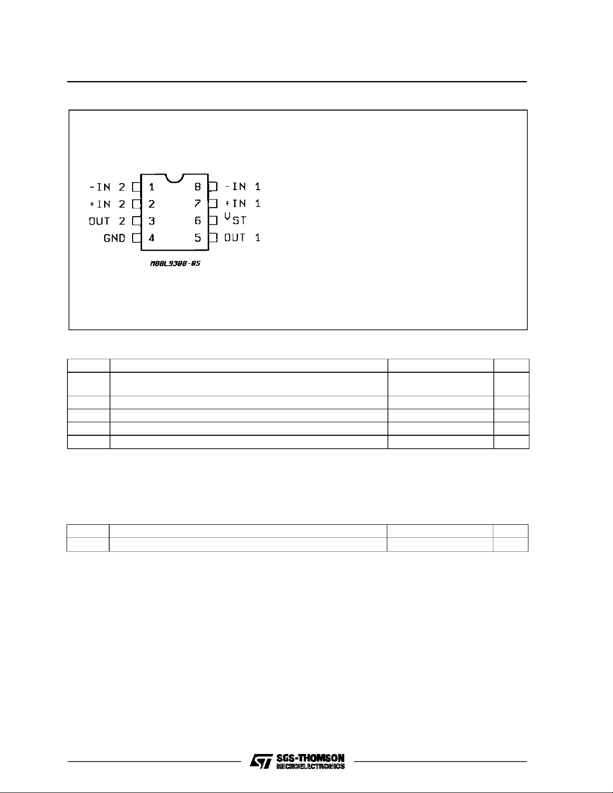
The L9308 is a monolithicinterface circuitwith differentialinput comparatorandopencollectoroutput
able to sink current specifically to drive lamps, relays,d.c. motors,electrovalvesetc.
Particularcarehas beentakentoprotectthedevice
againstdestructive failures- short circuit of outputs
, SOAprotection,supplyovervoltage.
to V
S
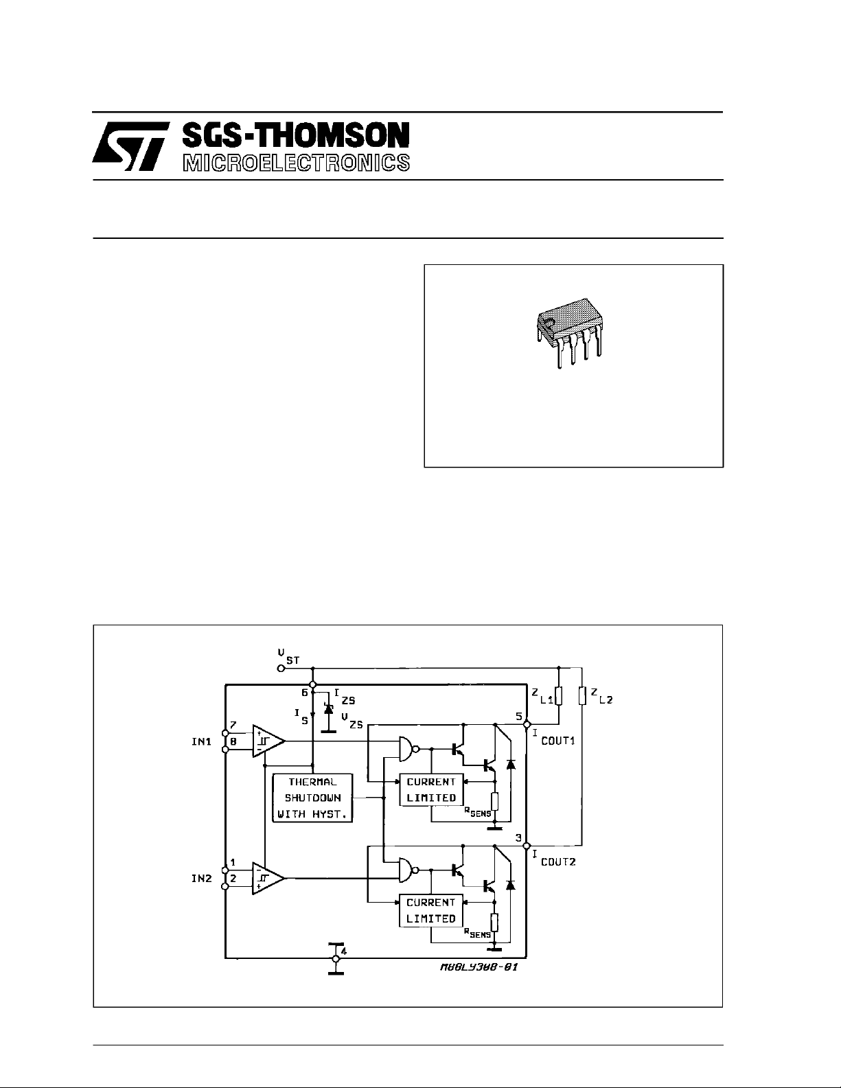
L9308
DUAL LOW SIDE DRIVER
MINIDIP
ORDERING NUMBER : L9308
A builtin thermalshut-downswitchesoffthedevice
whentheIC’sinternaldissipationbecomestoo high
and the chip temperature exceeds the security
threshold.
Theinputcomparatorhysteresisincreasestheinterface’s noise immunity allowing the correct use in
criticalenvironmentsas automotiveapplications.
BLOCK DIAGRAM
October1990
Thisis advanced informationon a new product now in development or undergoing evaluation. Details aresubject to change withoutnotice.
1/7
Page 2
L9308
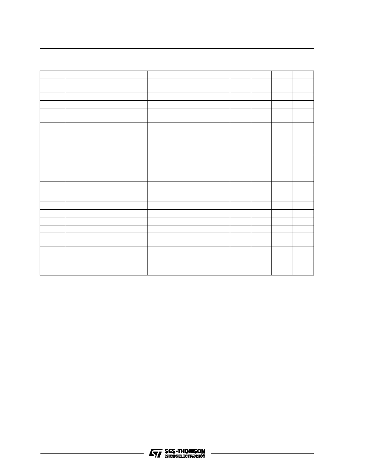
PIN CONNECTION (Top view)
ABSOLUTE MAXIMUM RATINGS
1) -IN2 Inverting input2
2) +IN2 Non-inverting input2
3) OUT2 Output2
4) GND Ground
5) OUT1 Output1
6) V
7) +IN1 Non-inverting input1
8) -IN1 Inverting input1
Supply
ST
Symbol Parameter Value Unit
Current Into Supply Tamb = 25°C, DC
I
ZS
Clamp Zener Diode Pulsed (*)
Supply Voltage 28 V(**)
V
S
Output Current Internally Limited
I
O
T
j,Tstg
(*) TON ≤ 2.5ms ; repetition time >30ms.
(**)Themaximum allowed supply voltage withoutlimitingresistor is limitedby thebuilt-in protectionzener diode : see V
values.If V
Junction and Storage Temperature – 55 to +150 °C
Power Dissipation at T
P
tot
ishigherthan VZSa resistorRSisnecessary to limit the zener currentIZS.
S
=85°C 650 mW
amb
30
80
ZS
spec.
THERMALDATA
Symbol Parameter Value Unit
R
th j-amb
Thermal Resistance Junction-ambient Max 100 °C/W
mA
mA
2/7
Page 3
L9308
ELECTRICALCHARACTERISTICS(Vs=14.4V;–40°C≤ T
, ≤85° C;RS=100Ω unlessotherwisenoted)
amb
Symbol Parameter Test Conditions Min. Typ. Max. Unit
Hysteresis of the Input
V
IH
Comparater
Input Bias Current V
I
B
Input Offset Current V
I
OS
CMR Input Common Mode Range V
Output Short Circuit Current for
I
SC
Each Channel
(see fig. 4)
V
I
I
V
I
V
Omin
On Status Saturation Voltage T
CSAT
Output Leakage Current V
I
OL
Supply voltage (pin 6) 3.5 18 V
ST
Supply Current V
”st.by”
Supply Current V
”ON”
Voltage Clamp Supply Protection IZS= 10mA 20 27 V
ZS
Minimum Output Current wiyth
VIN= 200mVpp ;
20 80 mV
f = 1kHz
+
–
=V
= 0 0.2 1.0 µA
I
I
+
–
=V
=0 ±50 ± 400 nA
I
I
= 6 – 18V
s
T
amb
=25°C
0V
VIN–VIN> 70mV
= 16V
V
S
=25°Cto85°C
T
amb
=–40°Cto25°C
T
amb
V
OUT 1, 2
amb
V
I
I
OUT 1, 2
T
amb
I
V
S
V
S
I
I
V
CSAT
=6V
=–40°Cto25°C
–
+
–V
> 70mV
I
= 300mA
1.0
=25°Cto85°C
–
–
–V
> 70mV
I
= 18V
10 300
=5V
+
–
V
> 70mV 5 8 mA
I
–
+
V
> 70mV 18 mA
I
= 1.5V 400 mA
–1.6 V
ST
0.6
0.7
1.2
1.5
1.4
20
the Outputs connected Together
Rise Time (see fig. 2)
t
r
t
Fall Time
f
don
doff
Delay Time on
Delay Time off
t
t
I
OUT
T
I
OUT
T
amb
amb
= 50mA
=25°C
= 50mA
=25°C
2
2
10
10
A
A
A
V
V
µA
µA
µs
µs
3/7
Page 4

L9308
Figure 1 : Switching Time TestCircuit. Figure 2 : SwitchingTime Waveforms for Resis-
tive Loads.
Figure 3 : Typical Applicationand TestCircuit.
Notes: a) R
b) C
4/7
S requiredonly to limit ΙZS
cut highfrequency gainduring current limiting.
1,C2
wheneverVSexceeds VZSvoltagevalue.
Page 5

Figure 4 : Typical SOACharacteristic.
L9308
5/7
Page 6

L9308
MINIDIP PACKAGE MECHANICAL DATA
DIM.
MIN. TYP. MAX. MIN. TYP. MAX.
A 3.32 0.131
a1 0.51 0.020
B 1.15 1.65 0.045 0.065
b 0.356 0.55 0.014 0.022
b1 0.204 0.304 0.008 0.012
D 10.92 0.430
E 7.95 9.75 0.313 0.384
e 2.54 0.100
e3 7.62 0.300
e4 7.62 0.300
F 6.6 0.260
I 5.08 0.200
L 3.18 3.81 0.125 0.150
Z 1.52 0.060
mm inch
6/7
Page 7

L9308
Information furnished is believed to be accurate and reliable. However, SGS-THOMSON Microelectronics assumes no responsibility for
the consequences of use of such information nor for any infringement of patents or other rights of third parties which may result from its
use. No license is granted by implication or otherwise under any patent or patent rights of SGS-THOMSON Microelectronics. Specifications mentioned in this publication are subject to change without notice. This publication supersedes and replaces all information previously supplied. SGS-THOMSON Microelectronics products are not authorized for use as critical components in life support devices or
systems without express written approval of SGS-THOMSON Microelectronics.
1994 SGS-THOMSON Microelectronics - All Rights Reserved
Australia - Brazil - France - Germany - Hong Kong - Italy - Japan - Korea - Malaysia - Malta - Morocco - The Netherlands - Singapore -
SGS-THOMSON Microelectronics GROUP OF COMPANIES
Spain - Sweden - Switzerland - Taiwan - Thaliand - United Kingdom - U.S.A.
7/7
 Loading...