

Page 1
DUALHIGH CURRENT RELAYDRIVER
.HIGH OUTPUT CURRENT
.HYSTERESIS INPUT COMPARATOR WITH
WIDERANGE COMMON MODE OPERATION
ANDGROUNDCOMPATIBLEINPUTS
.INPUTCOMPARATORHYSTERESIS
.INTERNAL THERMAL PROTECTION WITH
HYSTERESIS
.INTERNALOUTPUTOVERVOLTAGECLAMP-
ING
.SINGLESUPPLYVOLTAGE(3.5Vup to18V)
L9305A
Powerdip(8 + 8)
ORDERING NUMBER : L9305A
DESCRIPTION
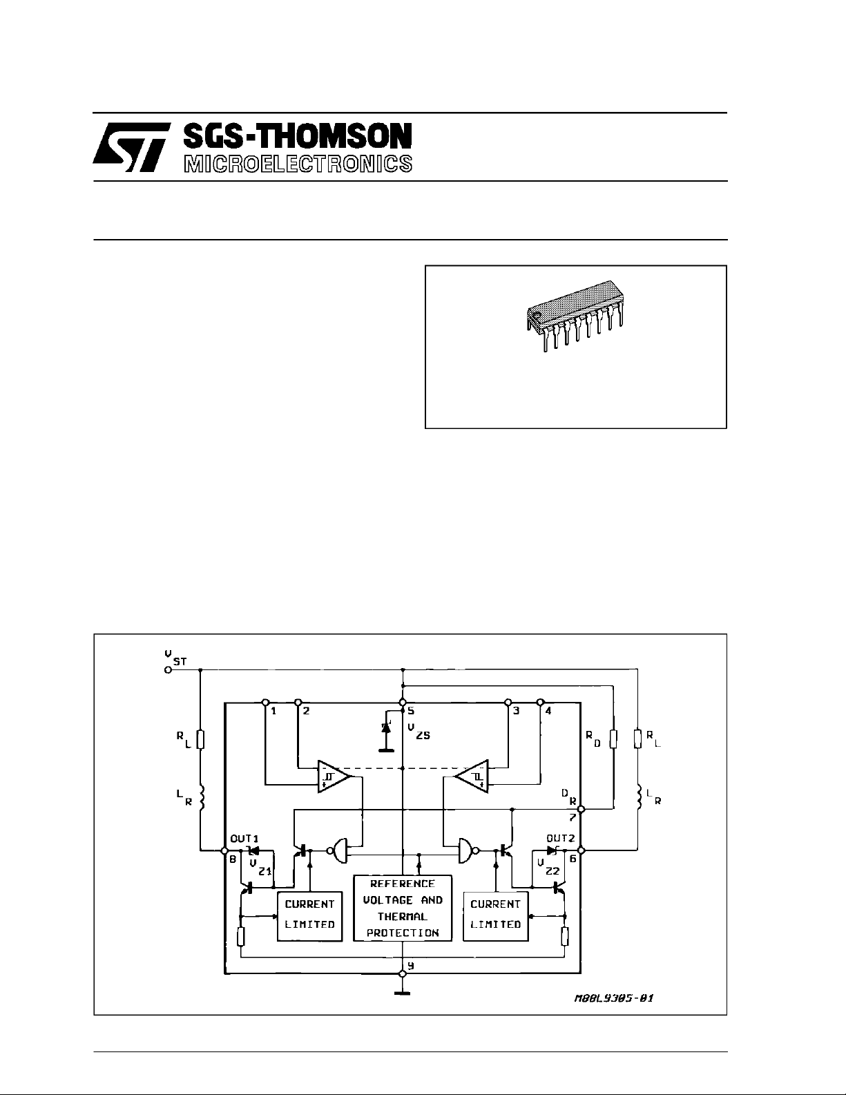
TheL9305Aisa monolithicinterfacecircuit withdifferentialinput comparatorandopencollectoroutput
ableto sink highcurrentspecifically todrive relays,
lamps,d.c. motors.
Particularcarehasbeen takento protectthedevice
againstdestructivefailures - shortcircuit ofoutputs
, outputovervoltages,supplyovervoltage.
toV
S
BLOCK DIAG RAM
A built inthermalshut-downswitchesoff thedevice
whentheIC’sinternaldissipationbecomestoogreat
and the chip temperature exceeds a set security
threshold.
A hysteresisinputcomparatorincreasestheinterface’snoiseimmunity, allowingthecorrectusealsoin
criticalenvironmentsasautomotiveor industrialapplications.
January1992
This is advanced information on a new product now in development or undergoing evaluation. Details are subject to change without notice.
1/6
Page 2
L9305A
ABSOLUTE MAXIMUM RATINGS
Symbol Parameter Value Unit
V
5
V
7
I
ZS
V
I
V
I
T
j,Tstg
P
tot
I
o
(*) The maximum allowed supply voltage without series resistors is limited by the built-in zener protection diodes
≤ 2.5 ms ; repetition time ≥ 30 m s.
(**) T
on
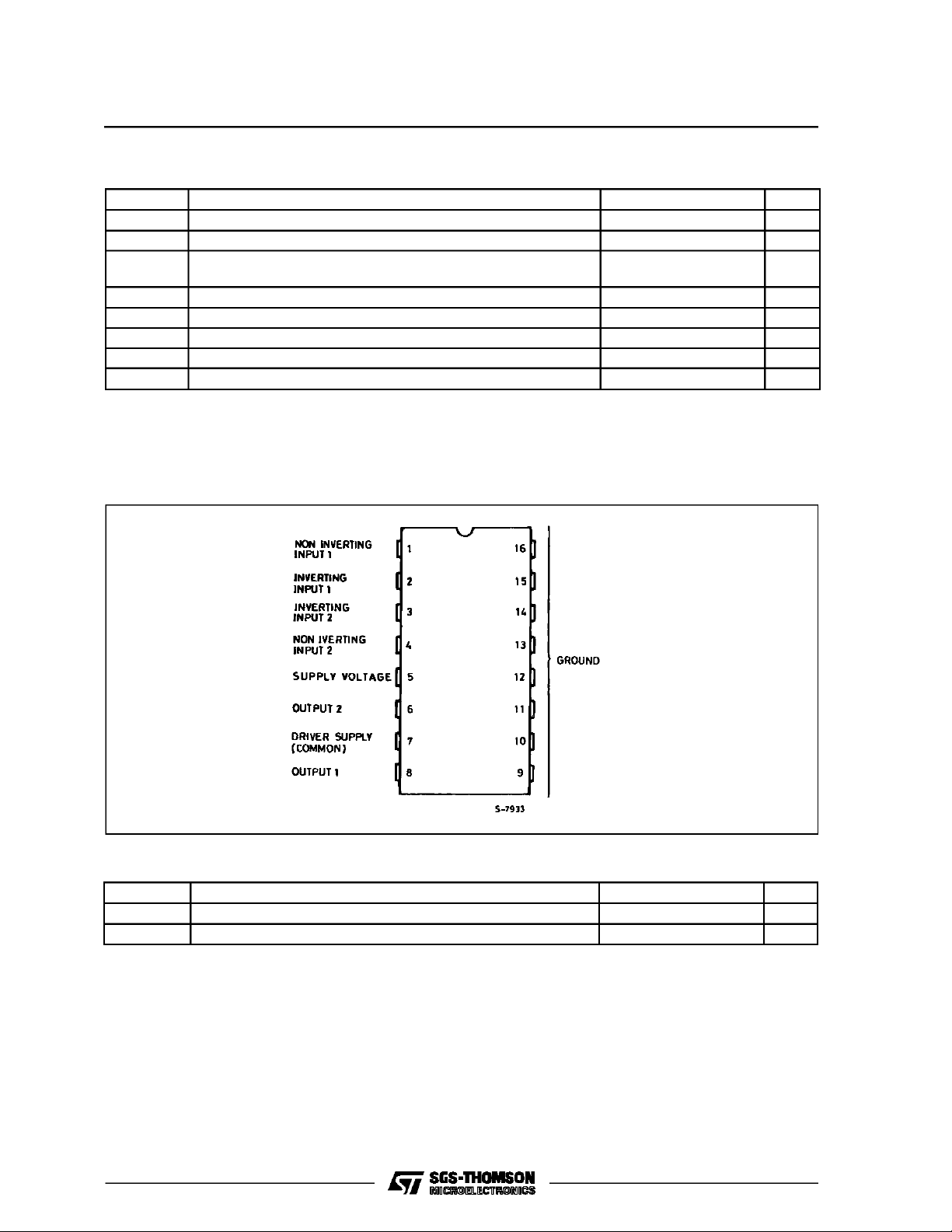
PIN CO NNECT IO N (top view)
Supply Voltage (*) 20 V
Driver Supply Voltage 26 V
Supply Zener Clamp Current (DC)
(PULSED) (**)
30
80
Comparator Input Voltage Range – 0.2 to 24 V
Differential Input Voltage 24 V
Junction and Storage Temperature – 55 to 150 °C
Power Dissipation at T
=85°C 928 mW
amb
Output Current Int. limited
mA
mA
THERMALDATA
Symbol Parameter Value Unit
Thermal Resistance Junction to pins Max. 15 °C/W
Thermal Resistance Junction to Ambient Max. 70 °C/W
2/6
R
th j-pins
R
th j-amb
Page 3

L9305A
ELECTRICAL CHARACTERISTICS (V5= 14.4V, T
=25°C ; refer to block diagramunless otherwise
amb
specified)
Symbol Parameter Test Conditions Min. Typ. Max. Unit
V
”st.by” Supply Current V
I
S
I
SON
V
V
V
I
I
OS
CMR Input Common Mode Range V
I
SC
I
CD
V
CSAT
I
OL
*TON≤ 2.5 ms ; repetition time ≥ 30 ms.
** The maximum allowed supply voltage without limiting resistors is limited by the built-in protection zener diodes see V
Spec. velues.
Supply Voltage 3.5 18* V
5
Supply Current V
Output Clamping Voltage (for
CZ
+
–
–V
≥70mV 5 8 mA
I
–
+
–V
> 70mV 18 30 mA
I
=1A 20 27 V
I
OUT
I
I
each channel)
Supply Voltage Clamp IZS= 10mA 20 27 V
ZS
Comparator Hysteresis V
IH
+
–
–V
I
=200mVpp
I
20 70 mV
f = 1kHz
Input Bias Current V+=V–= 0V 0.2 1 µA
B
Input Offset Current V+=V–=0V ±20 ± 200 nA
= 3.5V to 18V 0 V5–1.6 V
5
–
Output Short Circuit Current for
Each Channel
Driver Transistor Current
Capability
On Status Saturation Voltage V
Output Leakage Current V
V
V
I
CD
I
COUT
–V
I
–
–V
I
–
–V
I
= 100mA
= 1.2A
+
–V
I
+
≥70mV V
I
+
≥70mV DC
I
out
V
out
= 16.5V
=6V
Pulsed (**)
+
≥70mV
I
–
≥70mV 250 µA
I
0.85 A
2.5 A
300 mA
600 mA
1V
CZ,VZS
TEST AND APPLI CAT I ON CIRCUI T
3/6
Page 4

L9305A
APPLI CATI O N INF O RMATI ONS (refer to application circuit)
D1 andD2 diodes arerequiredonly for reversepolarityprotection.
If V
maybehigherthanVZSaresistorRSisneces-
S
sary to limitthe zener current I
mineR
1) <I
2) V
wherefromT
-V
valuethefollowingequationscanbeused:
S
V
S MAX–VD1–VZS min
R
S
S min–VD1–RS–ISON MAX>VST min
=25°C:
amb
SMAX
andV
arethemaximum and minimum
Smin
. Inorder to deter-
ZS
ZS MAX
valuesof power supplyvoltage
isthe forwarddiodeD1 voltagedrop
-V
D1
-V
-I
=20V
ZS min
=30 mAford.c.modeandI
ZS MAX
ZS MAX
=80mA
for pulsedmode (see Absolutemaximumratings)
-I
SOM MAX
-V
ST min
If no R
powerfullexternalzener D
=30mA
= 3.5 V
value can satisfy thesystem 1),2) a more
S
=18 Vis required.
Z
Then 1) becomes:
whereI
V
DZ MAX
voltagecannot be higher than 20 V otherwise
A
output overvoltage protection may be activated.
Morever V
A
protectionis required.
=22 to 24 V isa mandatoryforoutput 7protec-
D
Z2
tionif V
maybe higherthan26 V.
S
MOUNTINGINSTRUCTION
TheL9305Aisassembledina newplasticpackage,
thePowerdip,in which 8 pins (from 9 to 16) areattachedtotheframeandremoverthe heatproduced
by the chip.
Figure2and 3showtwo ways ofheatsinking.Inthe
first case, a PC board copper area is used as a
heatsinkI = 65 mm.While in the secondcase, the
device is solderedto an externalheatsink. In both
examples,the thermalresistancejunction-ambient
is35 °C/W.
V
S MAX–VD1
–18
R
S
<I
DZ MAX
isthe maximumallowedDZcurrent.
must be less than 16 V if short circuit
Figure2 : Exampleof HeatsinkUsingPC Board
Copper(I =65 mm).
Figure 3 : Exampleof an ExternalHeatsink.
4/6
Page 5

POWERDIP16PACKAGE MECHANICAL DATA
L9305A
DIM.
MIN. TYP. MAX. MIN. TYP. MAX.
a1 0.51 0.020
B 0.85 1.40 0.033 0.055
b 0.50 0.020
b1 0.38 0.50 0.015 0.020
D 20.0 0.787
E 8.80 0.346
e 2.54 0.100
e3 17.78 0.700
F 7.10 0.280
I 5.10 0.201
L 3.30 0.130
Z 1.27 0.050
mm inch
5/6
Page 6

L9305A
Information furnished is believed to be accurate and reliable. However, SGS-THOMSON Microelectronics assumes no responsibility for
the consequences of use of such information nor for any infringement of patents or other rights of third parties which may result from its
use. No license is granted by implication or otherwise under any patent or patent rights of SGS-THOMSON Microelectronics. Specifications mentioned in this publication are subject to change without notice. This publication supersedes and replaces all information previously supplied. SGS-THOMSON Microelectronics products are not authorized for use as critical components in life support devices or
systems without express written approval of SGS-THOMSON Microelectronics.
1994 SGS-THOMSON Microelectronics - All Rights Reserved
Australia - Brazil - France - Germany - Hong Kong - Italy- Japan - Korea - Malaysia - Malta - Morocco - The Netherlands - Singapore-
SGS-THOMSON Microelectronics GROUP OF COMPANIES
Spain - Sweden - Switzerland - Taiwan - Thaliand - United Kingdom - U.S.A.
6/6
 Loading...