

Page 1
QUAD INVERTING TRANSISTORSWITCH
.OUTPUT VOLTAGETO50V
.OUTPUT CURRENT TO 1.2A
.VERYLOWSATURATIONVOLTAGE
.TTL COMPATIBLEINPUTS
.INTEGRALSUPPRESSIONDIODE
L9222
DESCRIPTION
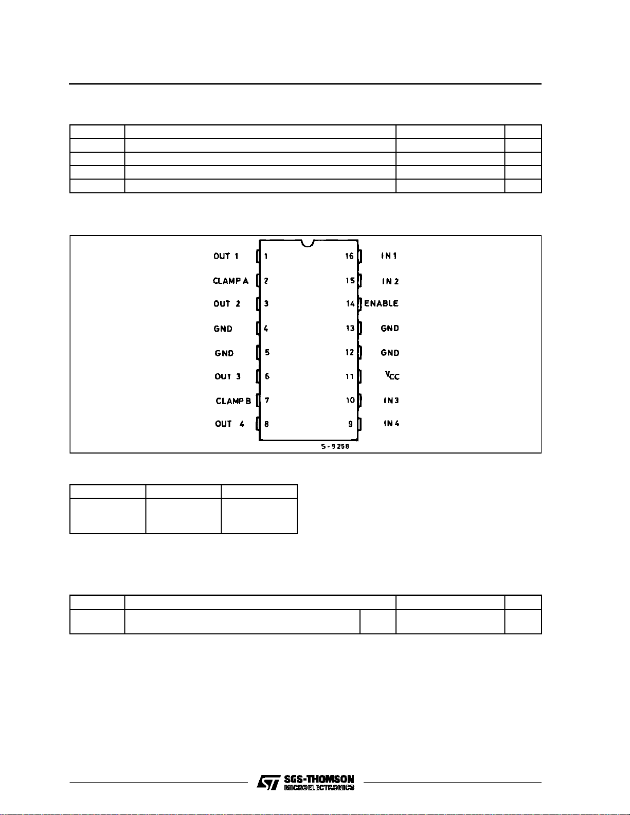
The L9222 monolithicquad transistorswitch is designedforhighcurrent,highvoltageswitchingapplications.
Eachof the fourswitchesis controlledby a logicinput andallfour are controlledby a commonenable
input. All inputs are TTL-compatiblefor direct connectionto logic circuits. Each switch consistsofan
open-collectortransistorplus a clamp diode for applicationswith inductiveloads.
BLOCK DIAGRAM
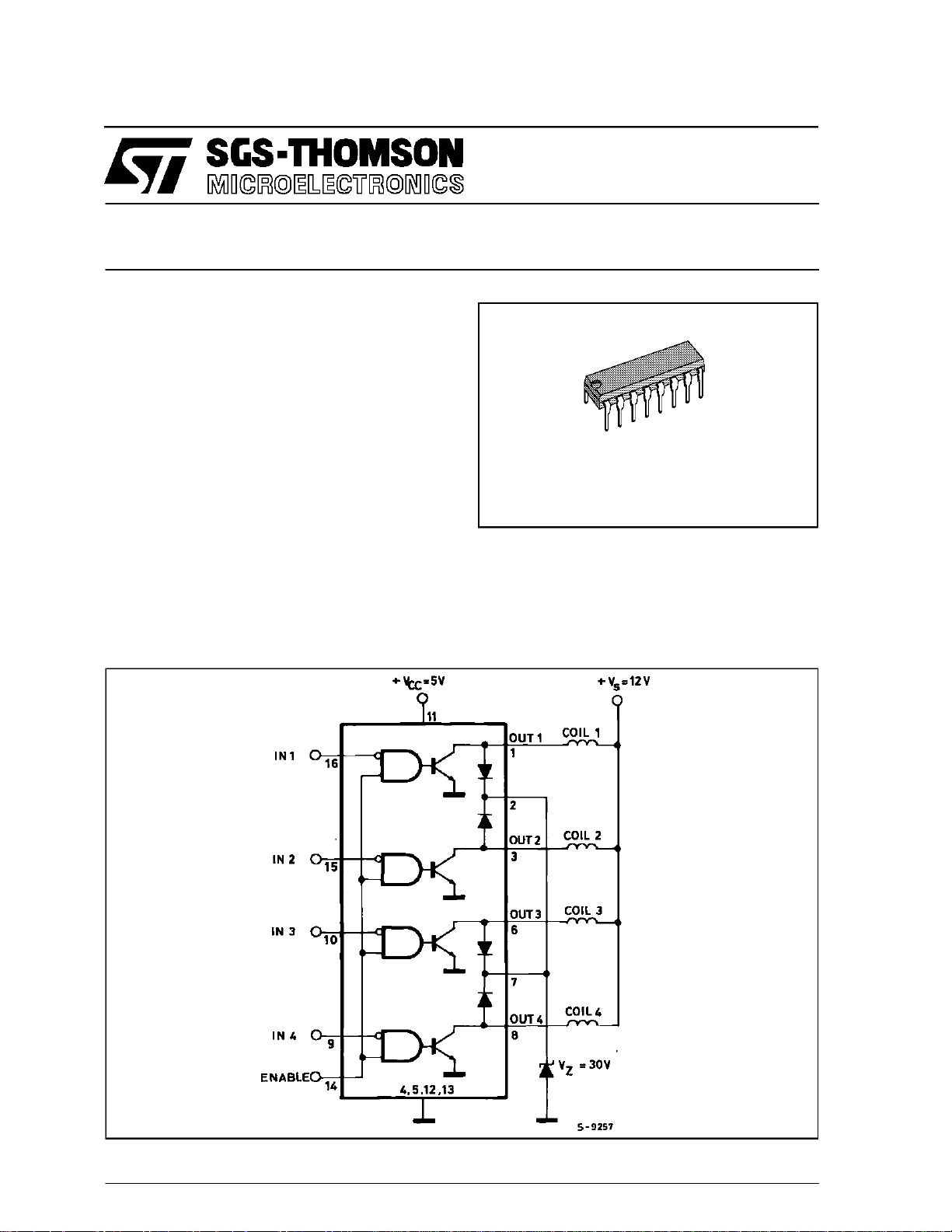
Powerdip(12+2+2)
ORDERING NUMBER : L9222
Theemitters ofthe four switches areconnectedtogether to GND. The switches of the same device
may be paralled. The device is intended to drive
coilssuchas relays,solenoids,unipolarsteppermotors,LED etc.
October1990
1/5
Page 2
L9222
ABSOLUTE MAXIMUM RATINGS
Symbol Parameter Value Unit
V
OUT
V
CC
V
T
j,TST
PI N CO NNECT I ON (top view)
Output Voltage – 0.7 to 50 V
Logic Supply Voltage 7 V
Input Voltage – 0.7 to VCC+ 0.3 V
i
Junction and Storage Temperature Range – 55 to 150 °C
TRUTH TABLE
Enable Input Power Out
H
H
L
F or each i nput : H= High level
L= Low level
X = Don’t care
L
H
X
ON
OFF
OFF
THERMAL DATA
Symbol Parameter Value Unit
R
th j-amb
R
th-J-case
Thermal Resistance Junction-ambient
Thermal Resistance Junction-case
Max
Max
90
14
°C/W
°C/W
2/5
Page 3

L9222
ELECTRICAL CHARACTERISTICS (VCC= 5Vdc ± 5% VEN=5V–40≤Tj≤125°C unless otherwise
specified)
Symbol Parameter Test Conditions Min. Typ. Max. Unit
V
CE(sus)
I
CEX
V
CE(sat)
V
IL
I
IL
V
IH
I
IH
Output Sustaining Voltage VIN=2VVEN= 2V, I
Output Leakage Current VCE= 50V
= 2V, VEN= 0.8V
V
IN
Collector Emitter Saturation VIN≥ 0.8V
= 0.1A
I
OUT
I
= 0.3A
OUT
= 0.6A; – 40 + 105°C
I
OUT
Input Low Voltage 0.8 V
Input Low Current VIN= 0.4V – 15 µA
Input High Voltage 2.0 V
Input High Current VIN≥ 2.0V – 15 µA
= 100mA 46 V
OUT
1mA
0.3
0.5
0.8
V
V
V
T
T
V
V
V
I
OUT
I
ENL
I
ENH
Logic Supply Current All Outputs ON I
I
S
= 06A 50 90 mA
OUT
All Outputs OFF 10 20 mA
Clamp Diode Leakage Current VR= 50V
I
R
Diode Reverse Voltage
Clamp Diode Forward Voltage IF= 0.6A 1.8 V
F
= 1.2A 2.0 V
I
F
Output Current VIN= 0.4V, R = 10Ω,VS= 13V 0.9 1.2 A
Propagation Delay Time
PHL
(high to low transition)
Propagation Delay Time
PHL
(low to high transition)
Low Enable Voltage 0.8 V
ENL
Tj=25°C
= 600mA
I
L
IL= 600mA
=25°C
T
j
Low Enable Current VEN= 0.4V – 15 µA
High Enable Voltage 2.0 V
ENH
High Enable Voltage VEN≥ 2.0V – 15 15 µA
100 µA
20 µs
20 µs
3/5
Page 4

L9222
POWERDIP16PACKAGE MECHANICAL DATA
DIM.
MIN. TYP. MAX. MIN. TYP. MAX.
a1 0.51 0.020
B 0.85 1.40 0.033 0.055
b 0.50 0.020
b1 0.38 0.50 0.015 0.020
D 20.0 0.787
E 8.80 0.346
e 2.54 0.100
e3 17.78 0.700
F 7.10 0.280
I 5.10 0.201
L 3.30 0.130
Z 1.27 0.050
mm inch
4/5
Page 5

L9222
Information furnished is believed to be accurate and reliable. However, SGS-THOMSON Microelectronics assumes no responsibility for
the consequences of use of such information nor for any infringement of patents or other rights of third parties which may result from its
use. No license is granted by implication or otherwise under any patent or patent rights of SGS-THOMSON Microelectronics. Specifications mentioned in this publication are subject to change without notice. This publication supersedes and replaces all information previously supplied. SGS-THOMSON Microelectronics products are not authorized for use as critical components in life support devices or
systems without express written approval of SGS-THOMSON Microelectronics.
1994 SGS-THOMSON Microelectronics - All Rights Reserved
Australia - Brazil - France - Germany - Hong Kong - Italy - Japan - Korea - Malaysia - Malta - Morocco - The Netherlands - Singapore -
SGS-THOMSON Microelectronics GROUP OF COMPANIES
Spain - Sweden - Switzerland - Taiwan - Thaliand - United Kingdom - U.S.A.
5/5
 Loading...