

Page 1
Features
■ 3 A DC output current
■ 4.5 V to 38 V input voltage
■ Output voltage adjustable from 0.6 V
■ 250 KHz switching frequency, programmable
up to 1 MHz
■ Internal soft-start and enable
■ Low dropout operation: 100% duty cycle
■ Voltage feed-forward
■ Zero load current operation
■ Overcurrent and thermal protection
■ VFQFPN3x3-10L and HSOP8 package
Applications
■ Consumer: STB, DVD, DVD recorder, car
audio, LCD TV and monitors
■ Industrial: PLD, PLA, FPGA, chargers
■ Networking: XDSL, modems, DC-DC modules
■ Computer: optical storage, hard disk drive,
printers, audio/graphic cards
■ LED driving
L7986
3 A step-down switching regulator
VFQFPN10 3 x 3 mm HSOP8 Exp. pad
Description
The L7986/A is a step-down switching regulator
with 3.7 A (minimum) current limited embedded
power MOSFET, so it is able to deliver up to 3 A
current to the load depending on the application
conditions.
The input voltage can range from 4.5 V to 38 V,
while the output voltage can be set starting from
0.6 V to V
Requiring a minimum set of external components,
the device includes an internal 250 kHz switching
frequency oscillator that can be externally
adjusted up to 1 MHz.
The QFN and the HSOP packages with exposed
pad allow reducing the R
and 40 °C/W respectively.
.
IN
down to 60 °C/W
thJA
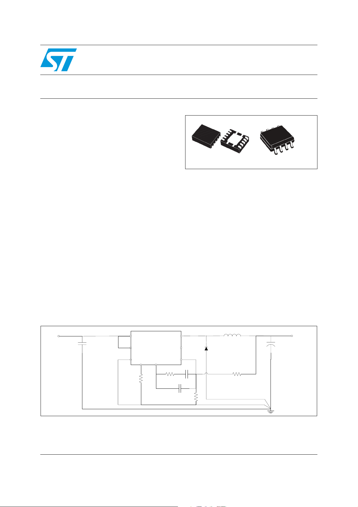
Figure 1. Application circuit
Vin=4.5V - 38V
VCC
9-10
C1
EN
43
L7986
GND FB
8
R5
6
7
COMPFSW
OUT
1-2
SYNCH
5
R4 R1
C4
C5
D1
R2
L1
March 2012 Doc ID 022450 Rev 2 1/44
Vout f rom 0.6 to Vin
C2
www.st.com
44
Page 2

Contents L7986
Contents
1 Pin settings . . . . . . . . . . . . . . . . . . . . . . . . . . . . . . . . . . . . . . . . . . . . . . . . 3
1.1 Pin connection . . . . . . . . . . . . . . . . . . . . . . . . . . . . . . . . . . . . . . . . . . . . . . 3
1.2 Pin description . . . . . . . . . . . . . . . . . . . . . . . . . . . . . . . . . . . . . . . . . . . . . . 3
2 Maximum ratings . . . . . . . . . . . . . . . . . . . . . . . . . . . . . . . . . . . . . . . . . . . . 4
3 Thermal data . . . . . . . . . . . . . . . . . . . . . . . . . . . . . . . . . . . . . . . . . . . . . . . 4
4 Electrical characteristics . . . . . . . . . . . . . . . . . . . . . . . . . . . . . . . . . . . . . 5
5 Functional description . . . . . . . . . . . . . . . . . . . . . . . . . . . . . . . . . . . . . . . 7
5.1 Oscillator and synchronization . . . . . . . . . . . . . . . . . . . . . . . . . . . . . . . . . . 8
5.2 Soft-start . . . . . . . . . . . . . . . . . . . . . . . . . . . . . . . . . . . . . . . . . . . . . . . . . . 10
5.3 Error amplifier and compensation . . . . . . . . . . . . . . . . . . . . . . . . . . . . . . 11
5.4 Overcurrent protection . . . . . . . . . . . . . . . . . . . . . . . . . . . . . . . . . . . . . . . 12
5.5 Enable function . . . . . . . . . . . . . . . . . . . . . . . . . . . . . . . . . . . . . . . . . . . . . 13
5.6 Hysteretic thermal shutdown . . . . . . . . . . . . . . . . . . . . . . . . . . . . . . . . . . 13
6 Application information . . . . . . . . . . . . . . . . . . . . . . . . . . . . . . . . . . . . . 14
6.1 Input capacitor selection . . . . . . . . . . . . . . . . . . . . . . . . . . . . . . . . . . . . . . 14
6.2 Inductor selection . . . . . . . . . . . . . . . . . . . . . . . . . . . . . . . . . . . . . . . . . . . 15
6.3 Output capacitor selection . . . . . . . . . . . . . . . . . . . . . . . . . . . . . . . . . . . . 17
6.4 Compensation network . . . . . . . . . . . . . . . . . . . . . . . . . . . . . . . . . . . . . . 18
6.4.1 Type III compensation network . . . . . . . . . . . . . . . . . . . . . . . . . . . . . . . 19
6.4.2 Type II compensation network . . . . . . . . . . . . . . . . . . . . . . . . . . . . . . . . 23
6.5 Thermal considerations . . . . . . . . . . . . . . . . . . . . . . . . . . . . . . . . . . . . . . 27
6.6 Layout considerations . . . . . . . . . . . . . . . . . . . . . . . . . . . . . . . . . . . . . . . . 28
6.7 Application circuit . . . . . . . . . . . . . . . . . . . . . . . . . . . . . . . . . . . . . . . . . . . 30
7 Application ideas . . . . . . . . . . . . . . . . . . . . . . . . . . . . . . . . . . . . . . . . . . . 34
7.1 Positive buck-boost . . . . . . . . . . . . . . . . . . . . . . . . . . . . . . . . . . . . . . . . . . 34
7.2 Inverting buck-boost . . . . . . . . . . . . . . . . . . . . . . . . . . . . . . . . . . . . . . . . . 36
2/44 Doc ID 022450 Rev 2
Page 3

L7986 Contents
8 Package mechanical data . . . . . . . . . . . . . . . . . . . . . . . . . . . . . . . . . . . . 38
9 Order codes . . . . . . . . . . . . . . . . . . . . . . . . . . . . . . . . . . . . . . . . . . . . . . . 41
10 Revision history . . . . . . . . . . . . . . . . . . . . . . . . . . . . . . . . . . . . . . . . . . . 42
Doc ID 022450 Rev 2 3/44
Page 4
Pin settings L7986
1 Pin settings
1.1 Pin connection
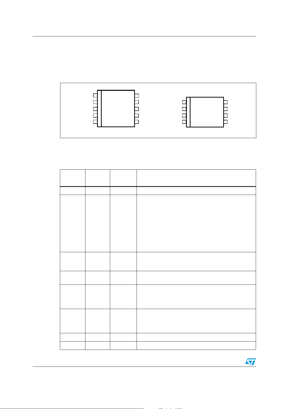
Figure 2. Pin connection (top view)
OUT
OUT
OUT
OUT
OUT
OUT
OUT
OUT
OUT
SYNCH
SYNCH
SYNCH
SYNCH
SYNCH
SYNCH
EN
EN
EN
COMP
COMP
COMP
COMP
COMP
COMP
VFQFPN10
VFQFPN10
1.2 Pin description
Table 1. Pin description
V
V
V
CCVCC
CCVCC
CCVCC
V
V
V
V
V
V
CC
CC
CC
CC
CC
CC
GND
GND
GND
GND
GND
GND
FSW
FSW
FSW
FSW
FSW
FSW
FB
FB
FB
FB
FB
FB
OUT
OUT
OUT
OUT
OUT
OUT
SYNCH
SYNCH
SYNCH
SYNCH
SYNCH
SYNCH
EN
EN
EN
COMP
COMP
COMP
COMP
COMP
COMP
HSOP8
HSOP8
V
V
V
V
V
V
CC
CC
CC
CC
CC
CC
GND
GND
GND
GND
GND
GND
FSW
FSW
FSW
FSW
FSW
FSW
FB
FB
FB
FB
FB
FB
N.
(VFQFPN)N.(HSOP)
Type Description
1-2 1 OUT Regulator output
Master/slave synchronization. When it is left floating, a
signal with a phase shift of half a period, with respect to the
power turn-on is present at the pin. When connected to an
external signal at a frequency higher than the internal one,
3 2 SYNCH
the device is synchronized by the external signal, with zero
phase shift.
Connecting together the SYNCH pin of two devices, the one
with a higher frequency works as master and the other one
as slave; so the two powers turn-ons have a phase shift of
half a period.
A logical signal (active high) enables the device. With EN
43EN
higher than 1.2 V the device is ON and with EN lower than
0.3 V the device is OFF.
54COMP
Error amplifier output to be used for loop frequency
compensation.
Feedback input. By connecting the output voltage directly to
65FB
this pin the output voltage is regulated at 0.6 V. To have
higher regulated voltages an external resistor divider is
required from Vout to the FB pin.
The switching frequency can be increased connecting an
76F
SW
external resistor from the FSW pin and ground. If this pin is
left floating, the device works at its free-running frequency of
250 KHz.
8 7 GND Ground
9-10 8 V
CC
Unregulated DC input voltage.
4/44 Doc ID 022450 Rev 2
Page 5
L7986 Maximum ratings
2 Maximum ratings
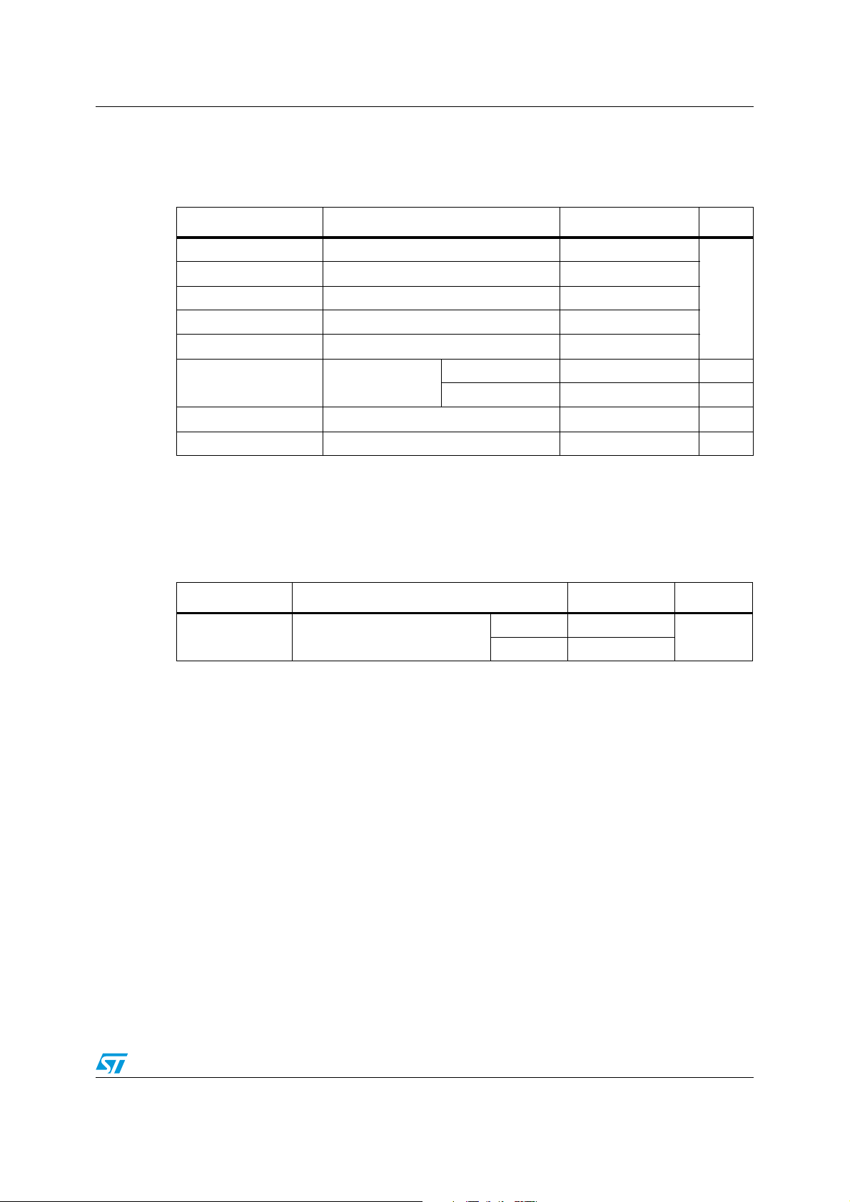
Table 2. Absolute maximum ratings
Symbol Parameter Value Unit
Vcc Input voltage 45
OUT Output DC voltage -0.3 to V
FSW, COMP, SYNCH Analog pin -0.3 to 4
EN Enable pin -0.3 to V
FB Feedback voltage -0.3 to 1.5
P
TOT
T
J
T
stg
3 Thermal data
Table 3. Thermal data
Symbol Parameter Value Unit
R
thJA
1. Package mounted on demonstration board.
Maximum thermal resistance
junction-ambient
CC
V
CC
Power dissipation
< 60 °C
at T
A
VFQFPN 1.5 W
HSOP 2
Junction temperature range -40 to 150 °C
Storage temperature range -55 to 150 °C
VFQFPN 60
(1)
HSOP 40
°C/W
Doc ID 022450 Rev 2 5/44
Page 6
Electrical characteristics L7986
4 Electrical characteristics
TJ = 25 °C, V
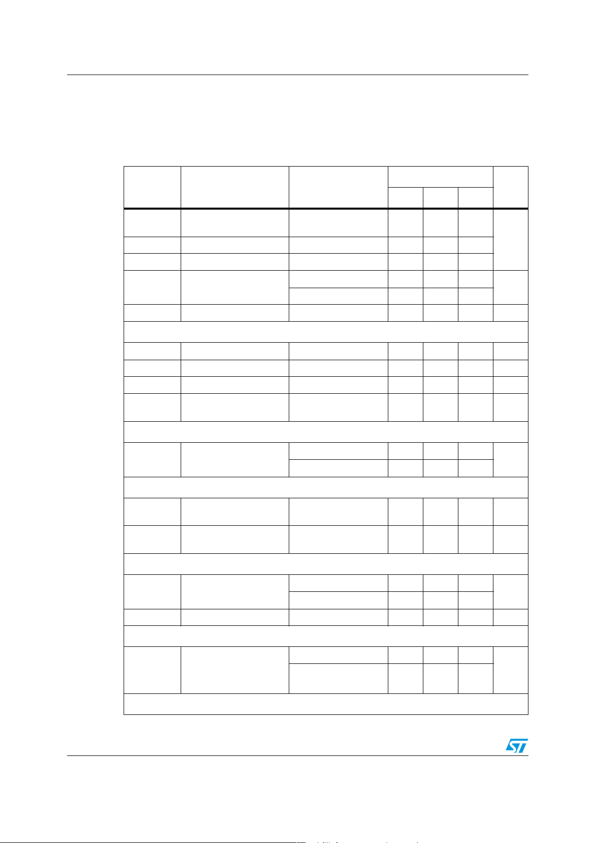
Table 4. Electrical characteristics
= 12 V, unless otherwise specified.
CC
Val ues
Symbol Parameter Test condition
Min. Typ. Max.
V
V
CCON
V
CCHYS
CC
Operating input voltage
range
Tur n - on VCC threshold
VCC UVLO Hysteseris
(1)
(1)
(1)
4.5 38
4.5
0.1 0.4
200
R
DSON
I
LIM
MOSFET on resistance
(1)
400
Maximum limiting current 3.7 4.2 4.7 A
Oscillator
(1)
210 250 275 KHz
V
F
SW
FSW
Switching frequency
FSW pin voltage 1.254 V
DDuty Cycle 0 100%
F
ADJ
Adjustable switching
frequency
R
=33 kΩ 1000 KHz
FSW
Unit
V
mΩ
Dynamic characteristics
V
FB
Feedback voltage
DC characteristics
I
Q
I
QST-BY
Quiescent current
Total standby quiescent
current
Enable
V
EN
I
EN
EN threshold voltage
EN current EN=V
Soft start
T
SS
Soft-start duration
Error amplifier
4.5 V<V
4.5 V<V
Duty cycle=0, V
V
<38 V 0.593 0.6 0.607
CC
(1)
CC
<38 V
FB
=0.8
0.582 0.6 0.618
2.4 mA
20 30 µA
Device OFF level 0.3
Device ON level 1.2
CC
7.5 10 µA
FSW pin floating 7.4 8.2 9.1
=1 MHz,
F
R
SW
FSW
=33 kΩ
2
V
V
ms
6/44 Doc ID 022450 Rev 2
Page 7
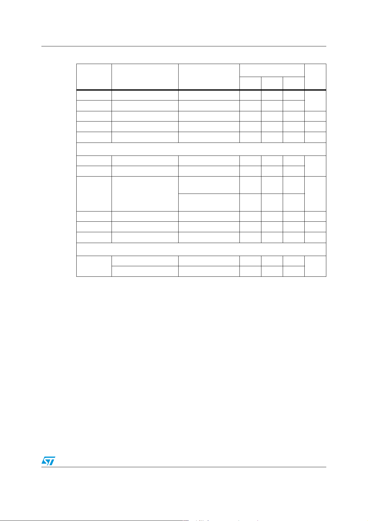
L7986 Electrical characteristics
Table 4. Electrical characteristics
Val ues
Symbol Parameter Test condition
Min. Typ. Max.
Unit
V
CH
V
CL
I
O SOURCE
I
O SINK
G
High level output voltage VFB<0.6 V 3
Low level output voltage VFB>0.6 V 0.1
Source COMP pin VFB=0.5 V, V
Sink COMP pin VFB=0.7 V, V
Open-loop voltage gain
V
Synchronization function
V
S_IN,HI
V
S_IN,LO
t
S_IN_PW
I
SYNCH,LO
V
S_OUT,HI
t
S_OUT_PW
High input voltage 2 3.3
Low input voltage 1
Input pulse width
Slave sink current V
Master output amplitude I
Output pulse width SYNCH floating 110 ns
Protection
Thermal shutdown 150
T
SHDN
Hystereris 30
(2)
V
S_IN,HI
V
S_IN,LO
V
S_IN,HI
V
S_IN,LO
SYNCH
SOURCE
V
=1 V 19 mA
COMP
=1 V 30 mA
COMP
100 dB
V
=3 V,
=0 V
100
ns
=2 V,
=1 V
300
=2.9 V 0.7 1 mA
=4.5 mA 2 V
°C
1. Specifications referred to TJ from -40 to +125 °C. Specifications in the -40 to +125 °C temperature range
are assured by design, characterization and statistical correlation.
2. Guaranteed by design.
Doc ID 022450 Rev 2 7/44
Page 8
Functional description L7986
5 Functional description
The L7986 is based on a “voltage mode”, constant frequency control. The output voltage
is sensed by the feedback pin (FB) compared to an internal reference (0.6 V) providing
V
OUT
an error signal that, compared to a fixed frequency sawtooth, controls the on- and off-time of
the power switch.
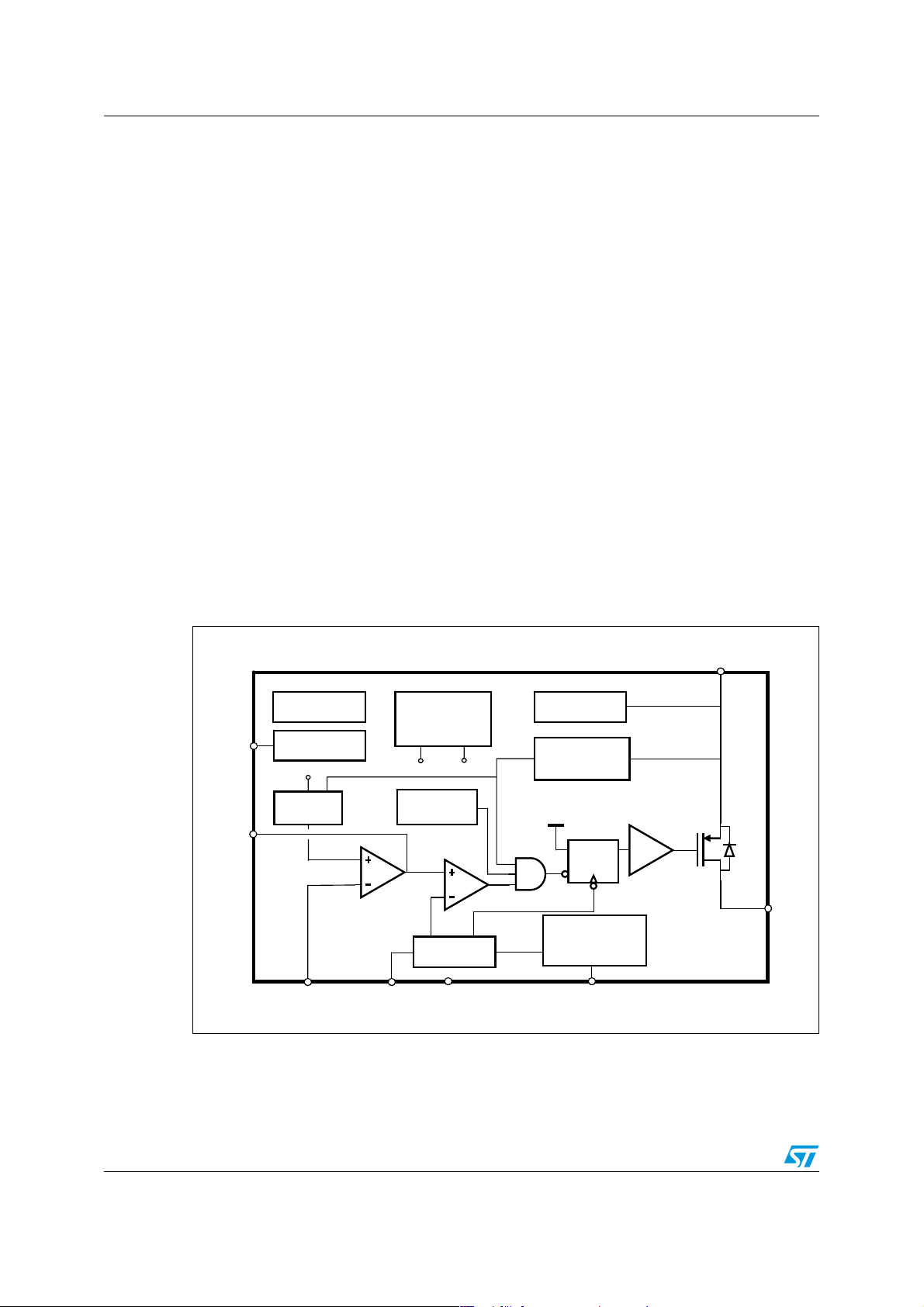
The main internal blocks are shown in the block diagram in Figure 3. They are:
● A fully integrated oscillator that provides sawtooth to modulate the duty cycle and the
synchronization signal. Its switching frequency can be adjusted by an external resistor.
The voltage and frequency feed-forward are implemented.
● The soft-start circuitry to limit inrush current during the startup phase.
● The voltage mode error amplifier.
● The pulse width modulator and the relative logic circuitry necessary to drive the internal
power switch.
● The high-side driver for embedded P-channel power MOSFET switch.
● The peak current limit sensing block, to handle overload and short-circuit conditions.
● A voltage regulator and internal reference. To supply the internal circuitry and provide a
fixed internal reference.
● A voltage monitor circuitry (UVLO) that checks the input and internal voltages.
● A thermal shutdown block, to prevent thermal runaway.
Figure 3. Block diagram
TRIMMING UVLO
TRIMMING UVLOUVLO
EN
EN
COMP
COMP
0.6V
0.6V
SOFT-
SOFT-
START
START
EN
EN
FB
FB
REGULATOR
REGULATOR
REGULATOR
&
&
&
BANDGAP
BANDGAP
BANDGAP
1.254V 3.3V
1.254V 3.3V
THERMAL
THERMAL
SHUTDOWN
SHUTDOWN
E/A
E/A
OSCILLATOR
OSCILLATOR
FSW
FSW
PWM
PWM
GND
GND
PEAK
PEAK
CURRENT
CURRENT
LIMIT
LIMIT
SRQ
SRQ
SYNCH
SYNCH
&
&
PHASE SHIFT
PHASE SHIFT
SYNCH
SYNCH
DRIVER
DRIVER
VCC
VCC
OUT
OUT
8/44 Doc ID 022450 Rev 2
Page 9
L7986 Functional description
5.1 Oscillator and synchronization
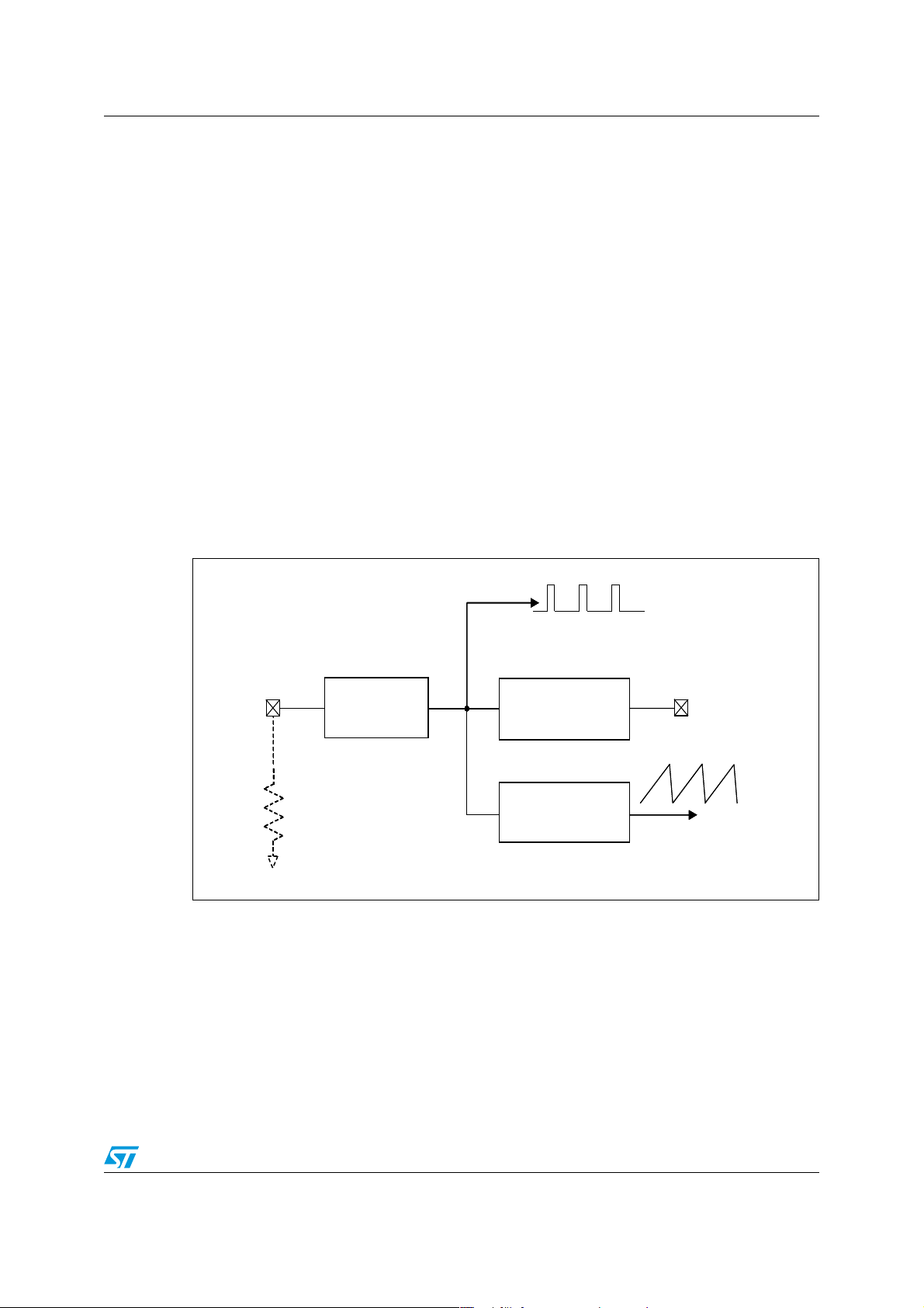
Figure 4 shows the block diagram of the oscillator circuit. The internal oscillator provides a
constant frequency clock. Its frequency depends on the resistor externally connected to the
FSW pin. If the FSW pin is left floating, the frequency is 250 kHz; it can be increased as
shown in Figure 6 by an external resistor connected to ground.
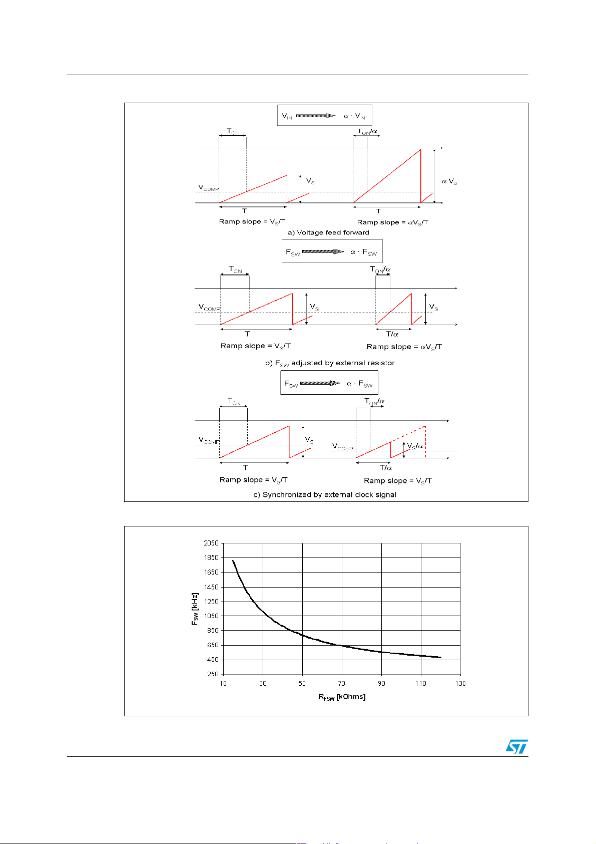
To improve the line transient performance, keeping the PWM gain constant versus the input
voltage, the voltage feed-forward is implemented by changing the slope of the sawtooth
according to the input voltage change (see Figure 5.a).
The slope of the sawtooth also changes if the oscillator frequency is increased by the
external resistor. In this way a frequency feed-forward is implemented (Figure 5.b) in order
to keep the PWM gain constant versus the switching frequency (see Section 6.4 for PWM
gain expression).
On the SYNCH pin the synchronization signal is generated. This signal has a phase shift of
180° with respect to the clock. This delay is useful when two devices are synchronized
connecting the SYNCH pins together. When SYNCH pins are connected, the device with a
higher oscillator frequency works as master, so the slave device switches at the frequency
of the master but with a delay of half a period. This minimizes the RMS current flowing
through the input capacitor (see the L5988D datasheet).
Figure 4. Oscillator circuit block diagram
Clock
ClockClock
FSW
FSW
The device can be synchronized to work at a higher frequency feeding an external clock
signal. The synchronization changes the sawtooth amplitude, changing the PWM gain
(Figure 5.c). This change must be taken into account when the loop stability is studied. To
minimize the change of PWM gain, the free-running frequency should be set (with a resistor
on the FSW pin) only slightly lower than the external clock frequency. This pre-adjusting of
the frequency changes the sawtooth slope in order to render the truncation of sawtooth
negligible, due to the external synchronization.
Clock
Clock
Generator
Generator
Synchronization
Synchronization
Ramp
Ramp
Generator
Generator
SYNCH
SYNCH
Sawtooth
Sawtooth
Doc ID 022450 Rev 2 9/44
Page 10
Functional description L7986
Figure 5. Sawtooth: voltage and frequency feed-forward; external synchronization
Figure 6. Oscillator frequency vs. FSW pin resistor
10/44 Doc ID 022450 Rev 2
Page 11
L7986 Functional description
5.2 Soft-start
The soft-start is essential to assure correct and safe startup of the step-down converter. It
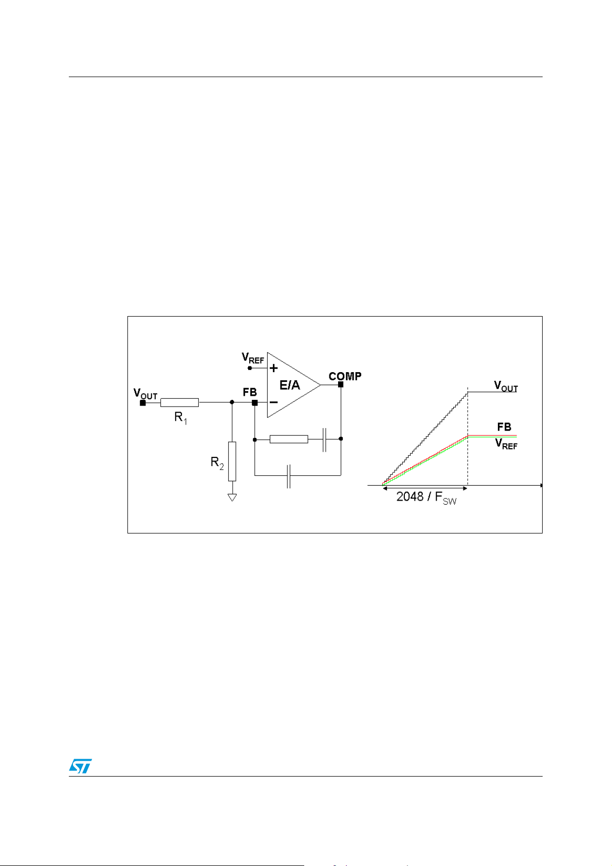
avoids inrush current surge and makes the output voltage increase monothonically.
The soft-start is performed by a staircase ramp on the non-inverting input (V
) of the error
REF
amplifier. So the output voltage slew rate is:
Equation 1
VREF
⎛⎞
1
------- -+
⋅=
⎝⎠
R2
where SR
SR
is the slew rate of the non-inverting input, while R1and R2 is the resistor
VREF
OUT
SR
R1
divider to regulate the output voltage (see Figure 7). The soft-start staircase consists of 64
steps of 9.5 mV each, from 0 V to 0.6 V. The time base of one step is of 32 clock cycles. So
the soft-start time and then the output voltage slew rate depend on the switching frequency.
Figure 7. Soft-start scheme
Soft-start time results:
Equation 2
32 64⋅
SS
TIME
--------------------=
Fsw
For example, with a switching frequency of 250 kHz, the SS
Doc ID 022450 Rev 2 11/44
TIME
is 8 ms.
Page 12
Functional description L7986
5.3 Error amplifier and compensation
The error amplifier (E/A) provides the error signal to be compared with the sawtooth to
perform the pulse width modulation. Its non-inverting input is internally connected to a 0.6 V
voltage reference, while its inverting input (FB) and output (COMP) are externally available
for feedback and frequency compensation. In this device the error amplifier is a voltage
mode operational amplifier, therefore, with high DC gain and low output impedance.
The uncompensated error amplifier characteristics are the following:
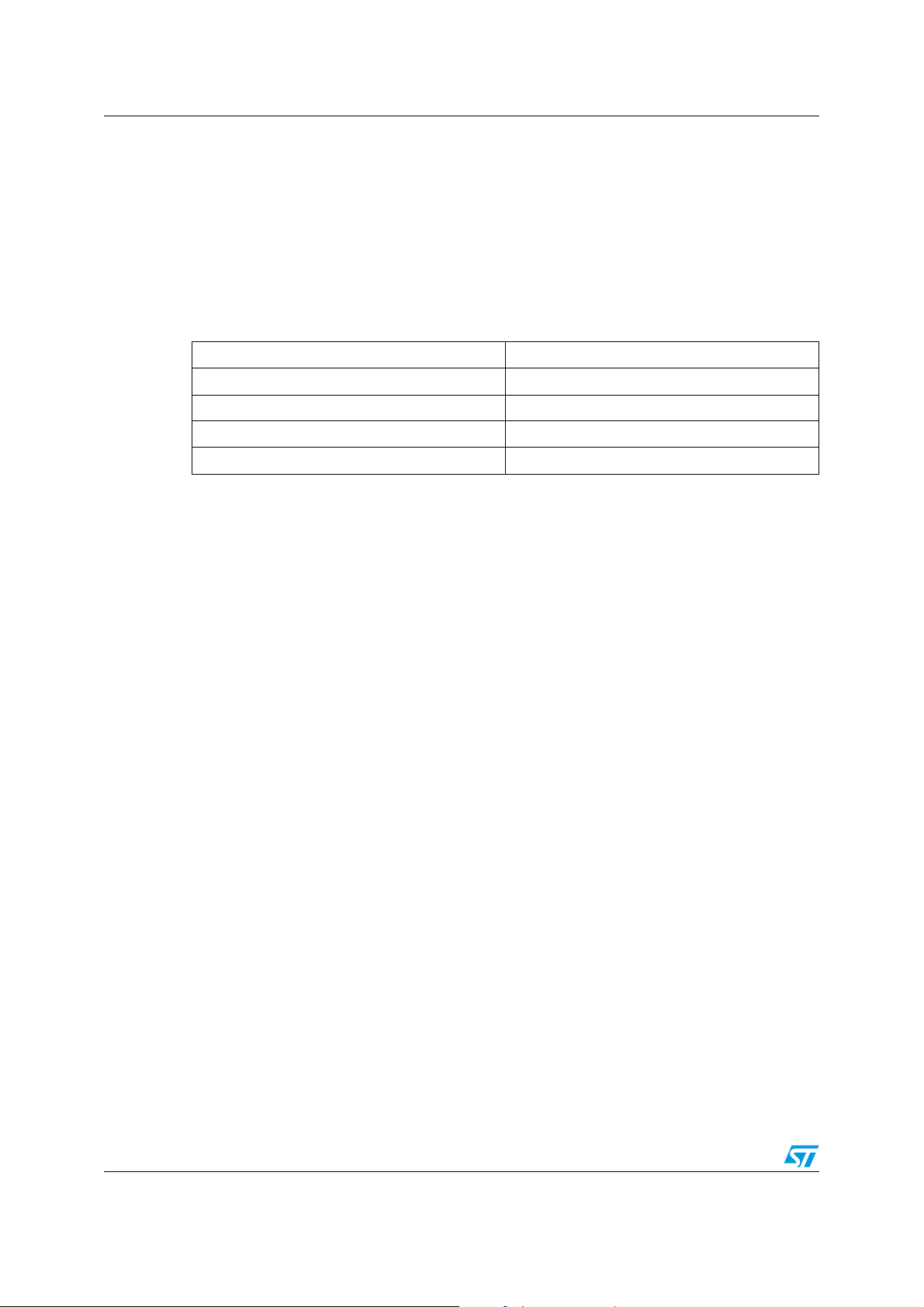
Table 5. Uncompensated error amplifier characteristics
Low frequency gain 100 dB
GBWP 4.5 MHz
Slew rate 7 V/µs
Output voltage swing 0 to 3.3 V
Maximum source/sink current 17 mA/25 mA
In continuous conduction mode (CCM), the transfer function of the power section has two
poles due to the LC filter and one zero due to the ESR of the output capacitor. Different
kinds of compensation networks can be used depending on the ESR value of the output
capacitor. If the zero introduced by the output capacitor helps to compensate the double
pole of the LC filter, a type II compensation network can be used. Otherwise, a type III
compensation network must be used (see Chapter 6.4 for details of the compensation
network selection).
Anyway, the methodology to compensate the loop is to introduce zeroes to obtain a safe
phase margin.
12/44 Doc ID 022450 Rev 2
Page 13

L7986 Functional description
5.4 Overcurrent protection
The L7986 implements overcurrent protection by sensing current flowing through the power
MOSFET. Due to the noise created by the switching activity of the power MOSFET, the
current sensing is disabled during the initial phase of the conduction time. This avoids an
erroneous detection of a fault condition. This interval is generally known as “masking time”
or “blanking time”. The masking time is about 200 ns.
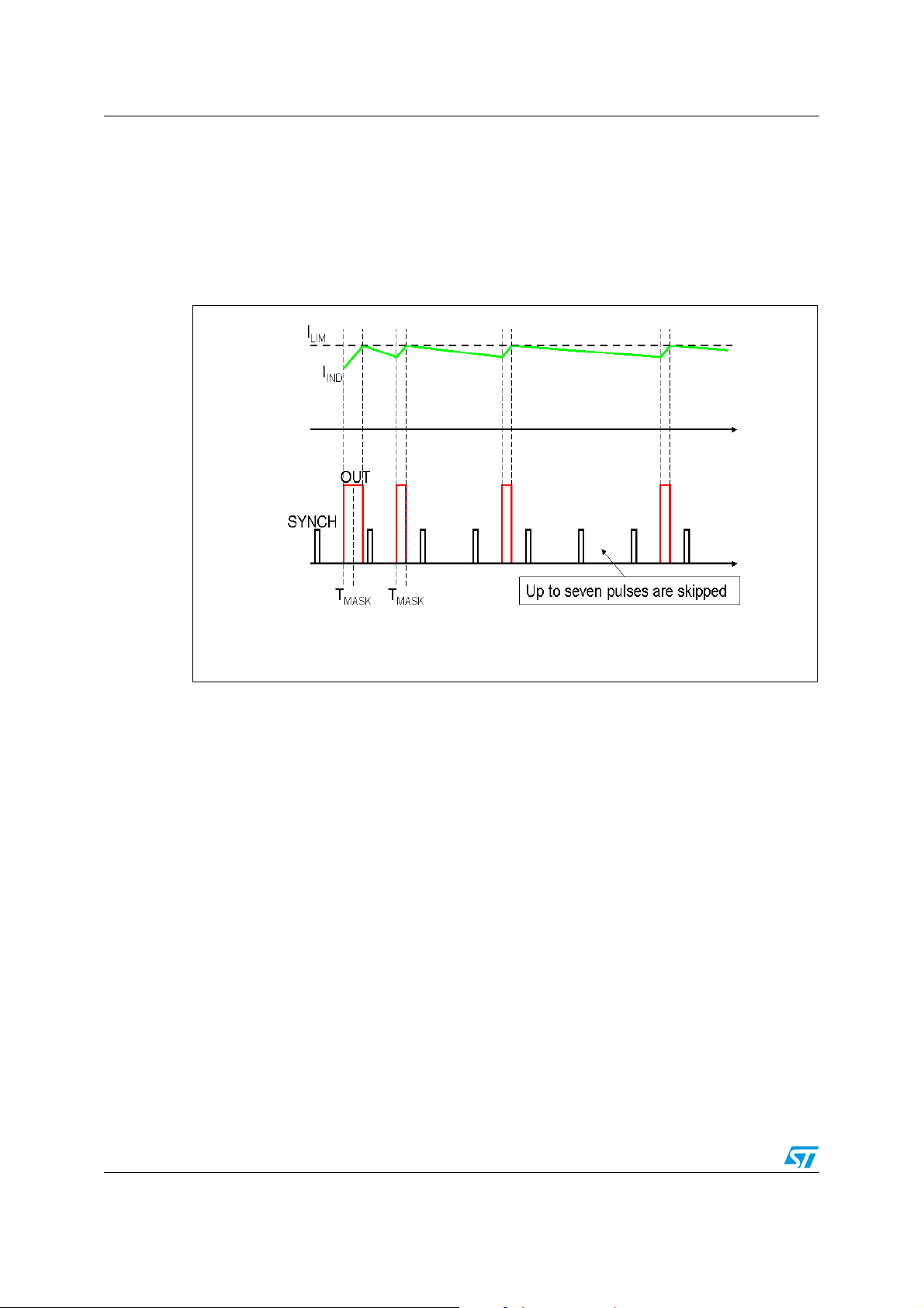
If the overcurrent limit is reached, the power MOSFET is turned off implementing pulse by
pulse overcurrent protection. In the overcurrent condition, the device can skip turn-on pulses
in order to keep the output current constant and equal to the current limit. If, at the end of the
“masking time”, the current is higher than the overcurrent threshold, the power MOSFET is
turned off and one pulse is skipped. If, at the following switching on, when the “masking
time” ends, the current is still higher than the overcurrent threshold, the device skips two
pulses. This mechanism is repeated and the device can skip up to seven pulses. While, if at
the end of the “masking time”, the current is lower than the overcurrent threshold, the
number of skipped cycles is decreased by one unit (see Figure 8).
So, the overcurrent/short-circuit protection acts by switching off the power MOSFET and
reducing the switching frequency down to one eighth of the default switching frequency, in
order to keep constant the output current around the current limit.
This kind of overcurrent protection is effective if the output current is limited. To prevent the
current from diverging, the current ripple in the inductor during the on-time must not be
higher than the current ripple during the off-time. That is:
Equation 3
VINV–
-------------------------------------------------------------- -----------------------------------------------------------
If the output voltage is shorted, V
OUT
R
⋅ DCR I
DSONIOUT
LF
⋅
SW
⋅––
OUT
OUT
≅ 0, I
V
OUTVFRDSONIOUT
--------------------------------------------------------------- --------------------------------------------------------
D⋅
OUT=ILIM
, D/FSW=T
⋅ DCR I
⋅
LF
SW
ON_MIN
, (1-D)/FSW≅ 1/FSW. So,
⋅++ +
OUT
1D–()⋅=
from Equation 3, the maximum switching frequency that guarantees to limit the current
results:
Equation 4
VFDCR I⋅+
With R
*
F
SW
=300 mΩ, DRC=0.08 Ω, the worst condition is with VIN=38 V, I
DSON
()
--------------------------------------------------------------- ----------------------
V
INRDSON
LIM
DCR+()I
⋅–()
LIM
------------------------ -
⋅=
T
ON_MIN
1
=3.7 A; the
LIM
maximum frequency to keep the output current limited during the short-circuit results 88
kHz.
The pulse-by-pulse mechanism, which reduces the switching frequency down to one eighth
the maximum F
, adjusted by the FSW pin, that assures a full effective output current
SW
limitation, is 88 kHz*8 = 706 kHz.
If, with V
= 38 V, the switching frequency is set higher than 706 kHz, during short-circuit
IN
condition the system finds a different equilibrium with higher current. For example, with
F
=800 kHz and the output shorted to ground, the output current is limited around:
SW
Doc ID 022450 Rev 2 13/44
Page 14
Functional description L7986
Equation 5
*
VINF
I
OUT
⋅ VFT
-------------------------------------------------------------- ------------------------------------------------------------- 4.2 A==
DRC T
⁄()R
SW
ON_MIN
⁄–
DSON
ON_MIN
DCR+()F
*
⋅+
SW
where F
* is 800 kHz divided by eight.
SW
Figure 8. Overcurrent protection
5.5 Enable function
The enable feature allows to put the device into standby mode. With the EN pin lower than
0.3 V the device is disabled and the power consumption is reduced to less than 30 µA. With
the EN pin lower than 1.2 V, the device is enabled. If the EN pin is left floating, an internal
pull-down ensures that the voltage at the pin reaches the inhibit threshold and the device is
disabled. The pin is also V
compatible.
CC
5.6 Hysteretic thermal shutdown
The thermal shutdown block generates a signal that turns off the power stage if the junction
temperature goes above 150 °C. Once the junction temperature returns to about 130 °C, the
device restarts in normal operation. The sensing element is very close to the PDMOS area,
so ensuring an accurate and fast temperature detection.
14/44 Doc ID 022450 Rev 2
Page 15

L7986 Application information
6 Application information
6.1 Input capacitor selection
The capacitor connected to the input must be capable of supporting the maximum input
operating voltage and the maximum RMS input current required by the device. The input
capacitor is subject to a pulsed current, the RMS value of which is dissipated over its ESR,
affecting the overall system efficiency.
So, the input capacitor must have an RMS current rating higher than the maximum RMS
input current and an ESR value compliant with the expected efficiency.
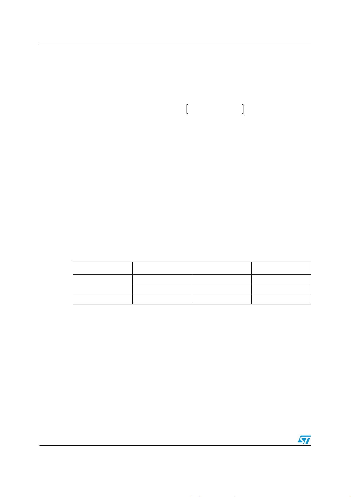
The maximum RMS input current flowing through the capacitor can be calculated as:
Equation 6
2
2D
I
RMSIO
⋅
D
----------------- -–
where Io is the maximum DC output current, D is the duty cycle, η is the efficiency.
Considering η=1, this function has a maximum at D=0.5 and it is equal to Io/2.
2
D
------ -+⋅=
2
η
η
In a specific application, the range of possible duty cycles must be considered in order to
find out the maximum RMS input current. The maximum and minimum duty cycles can be
calculated as:
Equation 7
V
+
OUTVF
MAX
---------------------------------------=
–
V
INMINVSW
D
and
Equation 8
V
+
OUTVF
-----------------------------------------=
V
–
INMAXVSW
where V
D
MIN
is the forward voltage on the freewheeling diode and VSW is the voltage drop
F
across the internal PDMOS.
The peak-to-peak voltage across the input capacitor can be calculated as:
Equation 9
V
PP
I
O
------------------------------
CINFSW⋅
D
⎛⎞
--- -–
1
⎝⎠
η
D
--- -
D
1D–()⋅+⋅ ESR I
η
⋅+⋅=
O
where ESR is the equivalent series resistance of the capacitor.
Doc ID 022450 Rev 2 15/44
Page 16
Application information L7986
Given the physical dimension, ceramic capacitors can well meet the requirements of the
input filter sustaining a higher input RMS current than electrolytic/tantalum types. In this
case the equation of C
as a function of the target VPP can be written as follows:
IN
Equation 10
C
IN
I
O
-------------------------------
VPPFSW⋅
D
⎛⎞
--- -–
1
⎝⎠
η
D
--- -
D
1D–()⋅+⋅⋅=
η
neglecting the small ESR of ceramic capacitors.
Considering η=1, this function has its maximum in D=0.5, therefore, given the maximum
peak-to-peak input voltage (V
PP_MAX
), the minimum input capacitor (C
IN_MIN
) value is:
Equation 11
I
O
⋅⋅
PP_MAXFSW
Typically C
of V
INMAX
C
IN_MIN
is dimensioned to keep the maximum peak-to-peak voltage in the order of 1%
IN
-------------------------------------------------------- -=
2V
.
In Table 6. some multi-layer ceramic capacitors suitable for this device are reported.
Table 6. Input MLCC capacitors
Manufacture Series Cap value (µF) Rated Voltage (V)
Taiyo Yuden
UMK325BJ106MM-T 10 50
GMK325BJ106MN-T 10 35
Murata GRM32ER71H475K 4.7 50
A ceramic bypass capacitor, as close to the VCC and GND pins as possible, so that
additional parasitic ESR and ESL are minimized, is suggested in order to prevent instability
on the output voltage due to noise. The value of the bypass capacitor can go from 100 nF to
1 µF.
6.2 Inductor selection
The inductance value fixes the current ripple flowing through the output capacitor. So the
minimum inductance value, in order to have the expected current ripple, must be selected.
The rule to fix the current ripple value is to have a ripple at 20%-40% of the output current.
In the continuous current mode (CCM), the inductance value can be calculated by the
following equation:
16/44 Doc ID 022450 Rev 2
Page 17
L7986 Application information
Equation 12
VINV
∆I
L
–
OUT
------------------------------- -
L
⋅
T
ON
+
V
OUTVF
-----------------------------
L
⋅==
T
OFF
where T
time of the external diode (in CCM, F
fixed V
calculate minimum duty). So, by fixing ∆I
is the conduction time of the internal high-side switch and T
ON
, is obtained at maximum T
OUT
=1/(TON + T
SW
which is at minimum duty cycle (see Section 6.1 to
OFF
=20% to 30% of the maximum output current, the
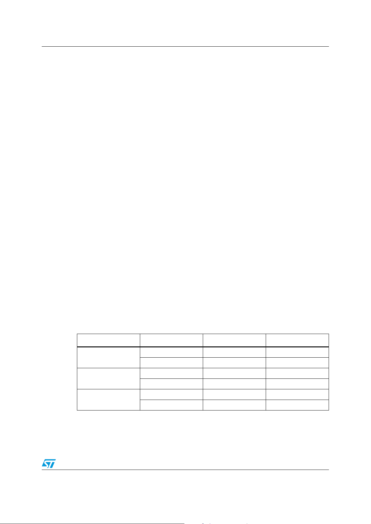
L
minimum inductance value can be calculated:
Equation 13
V
+
OUTVF
MIN
-----------------------------
∆I
MAX
where F
is the switching frequency, 1/(TON + T
SW
For example, for V
value to have ∆I
L
L
=5 V, VIN=24 V, IO=3 A and FSW=250 kHz, the minimum inductance
OUT
=30% of IO is about 18 µH.
The peak current through the inductor is given by:
Equation 14
I
LPK,
I
O
is the conduction
)). The maximum current ripple, at
OFF
1D
–
MIN
------------------------
⋅=
F
SW
).
OFF
∆I
L
--------+=
2
OFF
So, if the inductor value decreases, then the peak current (that must be lower than the
minimum current limit of the device) increases. According to the maximum DC output
current for this product family (3 A), the higher the inductor value, the higher the average
output current that can be delivered, without triggering the overcurrent protection.
In Ta bl e 7 some inductor part numbers are listed.
Table 7. Inductors
Manufacturer Series Inductor value (µH) Saturation current (A)
Coilcraft
Wurth
SUMIDA
MSS1038 3.8 to 10 3.9 to 6.5
MSS1048 12 to 22 3.84 to 5.34
PD Type L 8.2 to 15 3.75 to 6.25
PD Type M 2.2 to 4.7 4 to 6
CDRH6D226/HP 1.5 to 3.3 3.6 to 5.2
CDR10D48MN 6.6 to 12 4.1 to 5.7
Doc ID 022450 Rev 2 17/44
Page 18
Application information L7986
6.3 Output capacitor selection
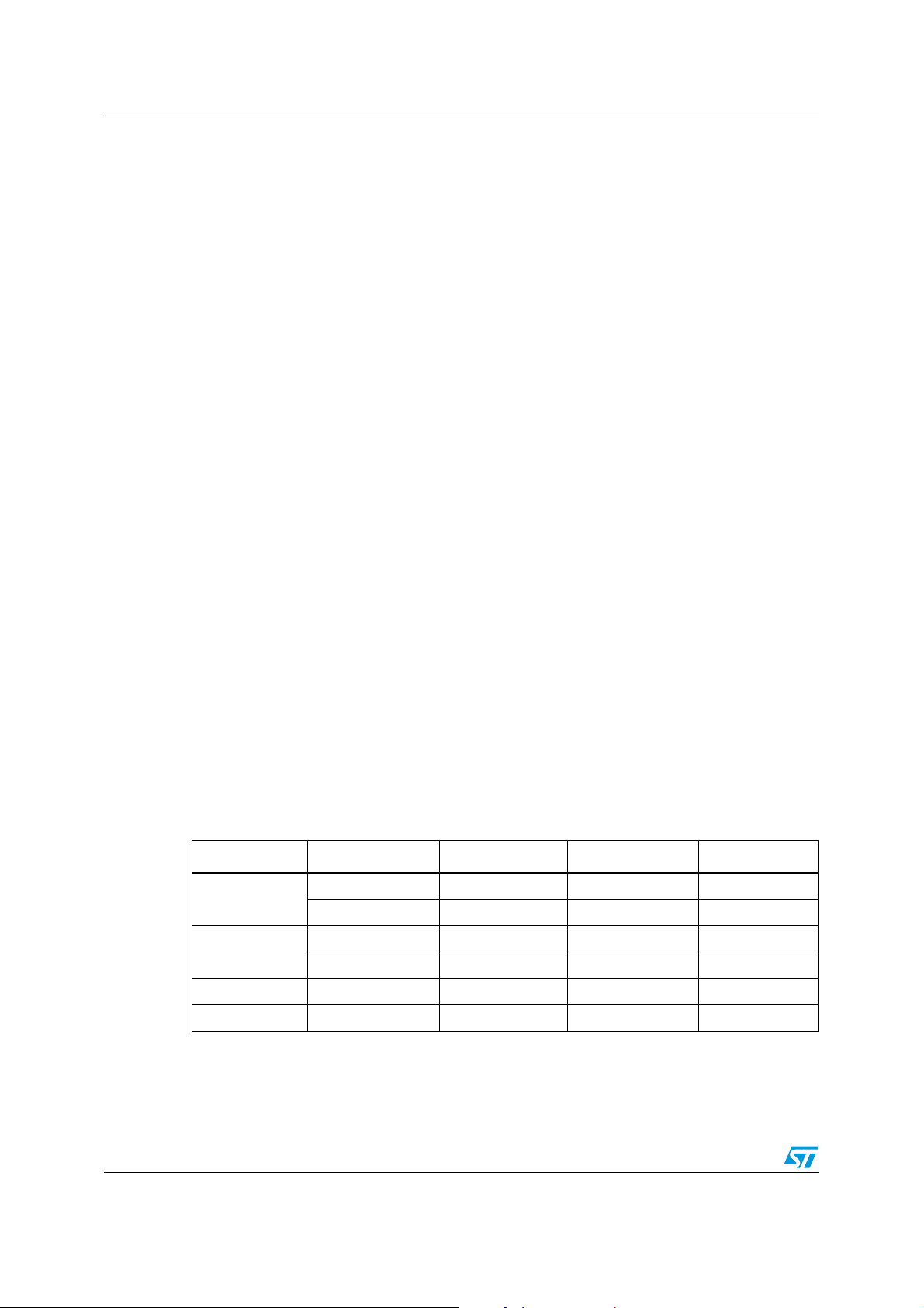
The current in the capacitor has a triangular waveform which generates a voltage ripple
across it. This ripple is due to the capacitive component (charge or discharge of the output
capacitor) and the resistive component (due to the voltage drop across its ESR). So the
output capacitor must be selected in order to have a voltage ripple compliant with the
application requirements.
The amount of the voltage ripple can be calculated starting from the current ripple obtained
by the inductor selection.
Equation 15
∆I
∆V
OUT
ESR ∆I
⋅
MAX
Usually the resistive component of the ripple is much higher than the capacitive one, if the
output capacitor adopted is not a multi-layer ceramic capacitor (MLCC) with very low ESR
value.
The output capacitor is important also for loop stability: it fixes the double LC filter pole and
the zero due to its ESR. Chapter 6.4 illustrates how to consider its effect in the system
stability.
MAX
---------------------------------------------+=
8C
⋅⋅
OUTfSW
For example, with V
to have a ∆V
OUT
=0.01·V
=5 V, VIN=24 V, ∆IL=0.9 A (resulting from the inductor value), in order
OUT
, if the multi-layer ceramic capacitors are adopted, 10 µF are
OUT
needed and the ESR effect on the output voltage ripple can be neglected. In the case of
non-negligible ESR (electrolytic or tantalum capacitors), the capacitor is chosen taking into
account its ESR value. So, in case of 330 µF with ESR=30 mΩ, the resistive component of
the drop dominates and the voltage ripple is 28 mV.
The output capacitor is also important to sustain the output voltage when a load transient
with high slew rate is required by the load. When the load transient slew rate exceeds the
system bandwidth, the output capacitor provides the current to the load. So, if the high slew
rate load transient is required by the application, the output capacitor and system bandwidth
must be chosen in order to sustain the load transient.
In Ta bl e 8 some capacitor series are listed.
Table 8. Output capacitors
Manufacturer Series Cap value (µF) Rated voltage (V) ESR (mΩ)
MURATA
PANASONIC
SANYO TPA/B/C 100 to 470 4 to 16 40 to 80
TDK C3225 22 to 100 6.3 < 5
GRM32 22 to 100 6.3 to 25 < 5
GRM31 10 to 47 6.3 to 25 < 5
ECJ 10 to 22 6.3 < 5
EEFCD 10 to 68 6.3 15 to 55
18/44 Doc ID 022450 Rev 2
Page 19
L7986 Application information
6.4 Compensation network
The compensation network must assure stability and good dynamic performance. The loop
of the L7986 is based on the voltage mode control. The error amplifier is a voltage
operational amplifier with high bandwidth. So, by selecting the compensation network the
E/A is considered as ideal, that is, its bandwidth is much larger than the system one.
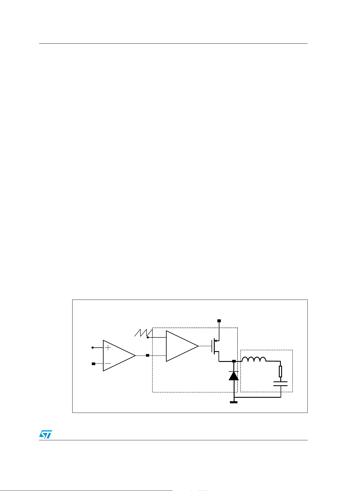
The transfer functions of the PWM modulator and the output LC filter are studied (see Figure
10.). The transfer function of the PWM modulator, from the error amplifier output (COMP
pin) to the OUT pin, results:
Equation 16
V
G
PW0
IN
---------=
V
s
where V
is the sawtooth amplitude. As seen in Chapter 5.1, the voltage feed-forward
S
generates a sawtooth amplitude directly proportional to the input voltage, that is:
Equation 17
V
KV
⋅=
S
IN
In this way the PWM modulator gain results constant and equal to:
Equation 18
V
1
IN
G
PW0
---------
V
s
--- - 18===
K
The synchronization of the device with an external clock provided through the SYNCH pin
can modify the PWM modulator gain (see Chapter 5.1 to understand how this gain changes
and how to keep it constant in spite of the external synchronization).
Figure 9. The error amplifier, the PWM modulator, and the LC output filter
V
V
CC
CC
V
V
FB
FB
REF
REF
E/A
E/A
V
V
S
S
COMP
COMP
PWM
PWM
L
OUT
OUT
G
G
PW0
PW0
Doc ID 022450 Rev 2 19/44
L
ESR
ESR
G
G
LC
LC
C
C
OUT
OUT
Page 20

Application information L7986
The transfer function on the LC filter is given by:
Equation 19
GLCs()
1
-------------------------------------------------------------- ---------------------=
++
1
---------------------------------- -
2π Qf⋅
⋅
s
s
------------------------------+
2π f
⋅
zESR
⎛⎞
---------------------- -
⎝⎠
2π f
LC
2
s
⋅
LC
where:
Equation 20
------------------------------------------------------- ----------------------------= f
f
LC
2π LC
1
⋅ 1
OUT
ESR
----------------+⋅⋅
R
OUT
zESR
---------------------------------------------------=,
2π ESR C
1
⋅⋅
OUT
Equation 21
R
-------------------------------------------------------- -----------------------------------------------
Q
OUT
LC
LC
OUTROUT
OUTROUT
ESR⋅⋅+
ESR+()⋅⋅ ⋅
R
OUT
V
OUT
--------------- -=,=
I
OUT
As seen in Chapter 5.3, two different kinds of network can compensate the loop. In the
following two paragraphs the guidelines to select the type II and type III compensation
network are illustrated.
6.4.1 Type III compensation network
The methodology to stabilize the loop consists of placing two zeroes to compensate the
effect of the LC double pole, therefore increasing phase margin; then, to place one pole in
the origin to minimize the dc error on regulated output voltage; and finally, to place other
poles far from the zero dB frequency.
If the equivalent series resistance (ESR) of the output capacitor introduces a zero with a
frequency higher than the desired bandwidth (that is: 2π∗ ESR∗COUT<1/BW), the type III
compensation network is needed. Multi-layer ceramic capacitors (MLCC) have very low
ESR (<1 mΩ), with very high frequency zero, so a type III network is adopted to compensate
the loop.
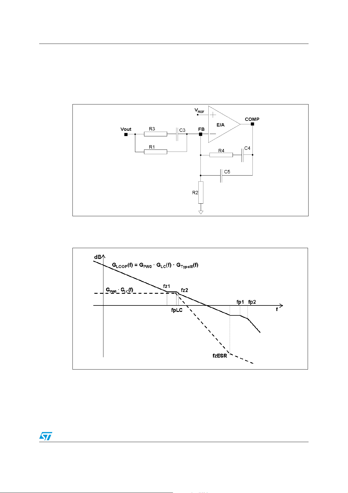
In Figure 10 the type III compensation network is shown. This network introduces two
zeroes (f
Equation 22
20/44 Doc ID 022450 Rev 2
, fZ2) and three poles (fP0, fP1, fP2). They are expressed as:
Z1
f
-------------------------------------------------------= f
Z1
2π C
1
+()⋅⋅
3R1R3
Z2
------------------------------------=,
2π R
⋅⋅
1
4C4
Page 21
L7986 Application information
Equation 23
fP00= f
1
------------------------------------= f
P1
⋅⋅
2π R
3C3
---------------------------------------------------=,,
P2
2π R
1
C4C5⋅
--------------------- -
⋅⋅
4
C
+
4C5
Figure 10. Type III compensation network
In Figure 11 the Bode diagram of the PWM and LC filter transfer function (G
and the open-loop gain (G
LOOP
(f)=G
· GLC(f) · G
PW0
(f)) are drawn.
TYPEIII
PW0
· GLC(f))
Figure 11. Open-loop gain: module Bode diagram
The guidelines for positioning the poles and the zeroes and for calculating the component
values can be summarized as follows:
1. Choose a value for R
2. Choose a gain (R
, usually between 1 kΩ and 5kΩ.
1
) in order to have the required bandwidth (BW), that means:
4/R1
Doc ID 022450 Rev 2 21/44
Page 22

Application information L7986
Equation 24
BW
--------- -
R
4
f
LC
⋅⋅=
KR
1
where K is the feed-forward constant and 1/K is equal to 18.
3. Calculate C
by placing the zero at 50% of the output filter double pole frequency (fLC):
4
Equation 25
1
--------------------------------- -=
π R
⋅⋅
4fLC
4. Calculate C
C
4
by placing the second pole at four times the system bandwidth (BW):
5
Equation 26
C
--------------------------------------------------------------- ----------=
C
5
2π R4C44BW⋅ 1–⋅⋅⋅
4
5. Set also the first pole at four times the system bandwidth and also the second zero at
the output filter double pole:
Equation 27
R
R
3
1
------------------------------= C
4BW⋅
-------------------- 1–
f
LC
3
-------------------------------------------------=,
2π R
1
3
4BW⋅⋅⋅
The suggested maximum system bandwidth is equal to the switching frequency divided by
3.5 (F
For example, with V
/3.5), anyway, lower than 100 kHz if the FSW is set higher than 500 kHz.
SW
=5 V, VIN=24 V, IO=3 A, L=18 µH, C
OUT
=22 µF, E S R < 1 m Ω, the type
OUT
III compensation network is:
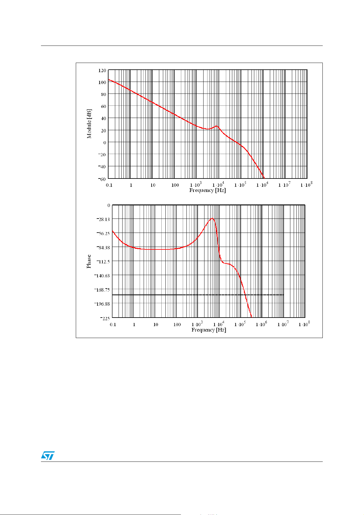
4.99k Ω= R2680Ω= R3200Ω= R42kΩ= C33.3n F= C422nF= C5220pF=,,,, ,,
R
1
In Figure 12 the module and phase of the open-loop gain is shown. The bandwidth is about
58 kHz and the phase margin is 50°.
22/44 Doc ID 022450 Rev 2
Page 23
L7986 Application information
Figure 12. Open-loop gain Bode diagram with ceramic output capacitor
Doc ID 022450 Rev 2 23/44
Page 24
Application information L7986
6.4.2 Type II compensation network
If the equivalent series resistance (ESR) of the output capacitor introduces a zero with a
frequency lower than the desired bandwidth (that is: 2π∗ESR∗COUT>1/BW), this zero helps
stabilize the loop. Electrolytic capacitors show non-negligible ESR (>30 mΩ), so with this
kind of output capacitor the type II network combined with the zero of the ESR allows to
stabilize the loop.
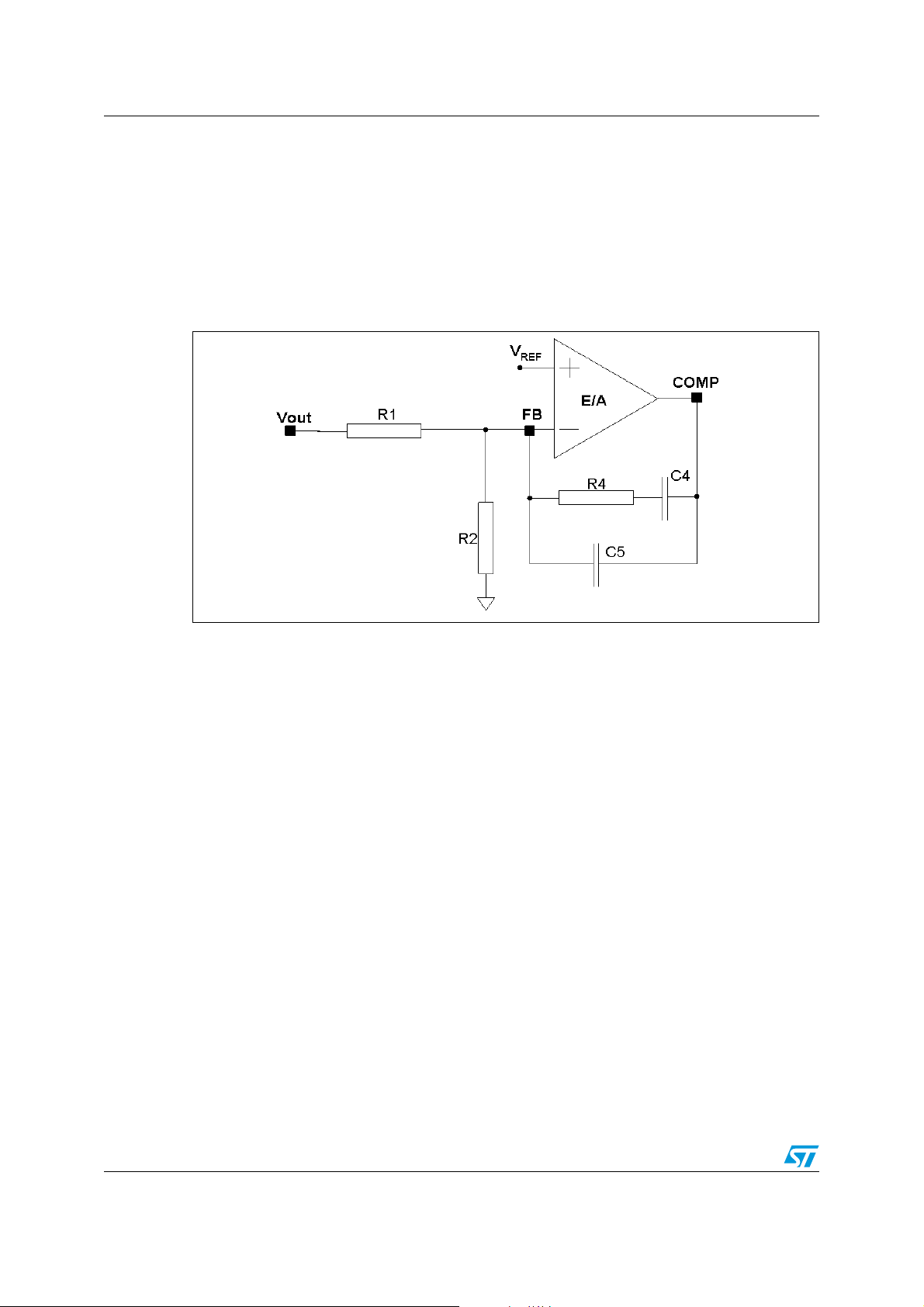
In Figure 13 the type II network is shown.
Figure 13. Type II compensation network
The singularities of the network are:
------------------------------------= f
f
Z1
2π R
⋅⋅
1
4C4
P0
0= f
P1
---------------------------------------------------=,,
2π R
1
C4C5⋅
--------------------- -
⋅⋅
4
C
+
4C5
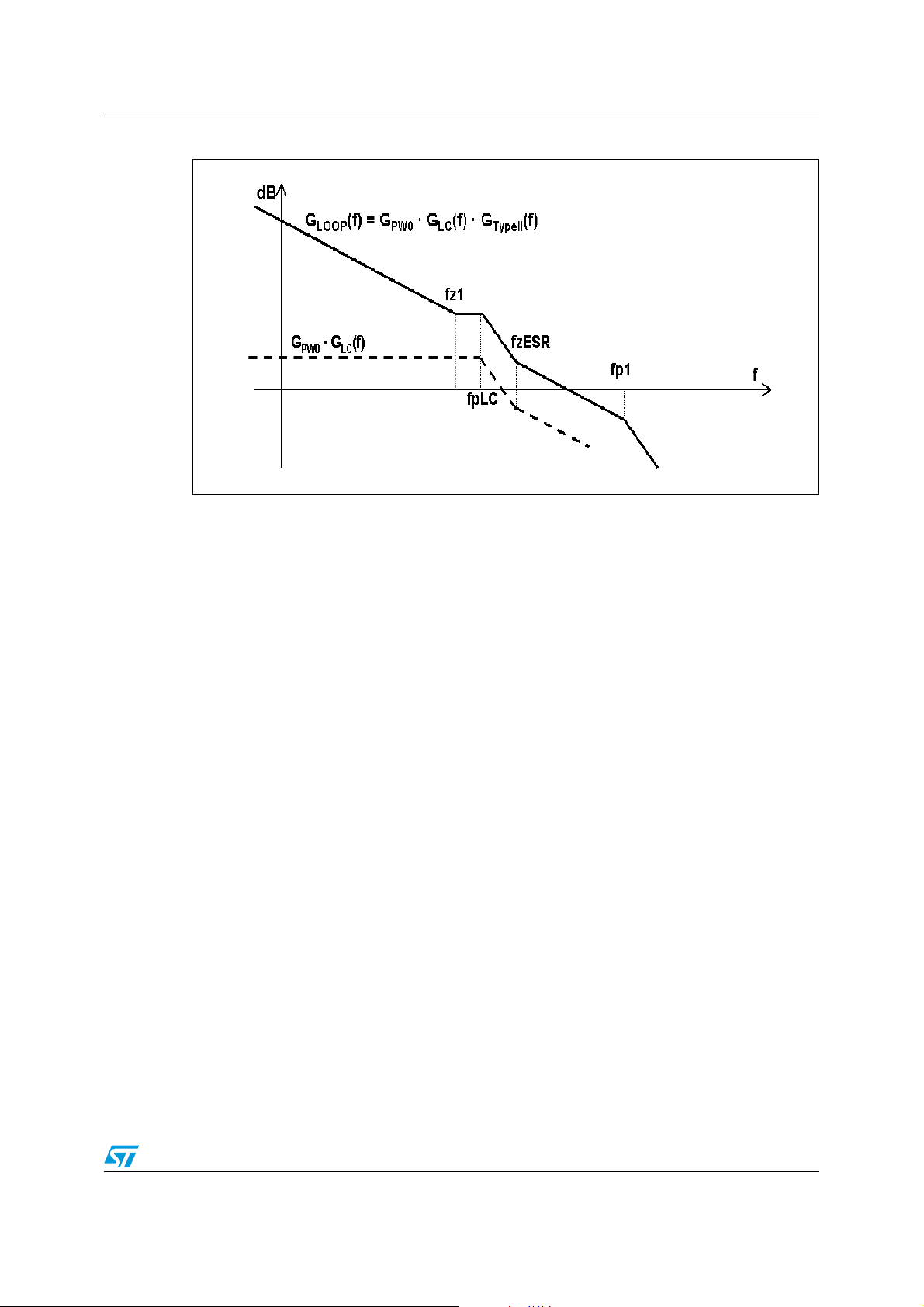
In Figure 14 the Bode diagram of the PWM and LC filter transfer function (G
and the open-loop gain (G
LOOP
(f)=G
· GLC(f) · G
PW0
(f)) are drawn.
TYPEII
PW0
· GLC(f))
24/44 Doc ID 022450 Rev 2
Page 25
L7986 Application information
Figure 14. Open-loop gain: module Bode diagram
The guidelines for positioning the poles and the zeroes and for calculating the component
values can be summarized as follows:
1. Choose a value for R
, usually between 1 kΩ and 5 kΩ, in order to have values of C4
1
and C5 not comparable with parasitic capacitance of the board.
2. Choose a gain (R
) in order to have the required bandwidth (BW), that means:
4/R1
Equation 28
where f
is the ESR zero:
ESR
R
4
2
f
⎛⎞
ESR
-------------
⎜⎟
⎝⎠
⋅⋅⋅=
f
LC
-------------
f
BW
ESR
V
---------
V
S
R
1
IN
Equation 29
f
ESR
---------------------------------------------------=
2π ESR C
1
⋅⋅
OUT
and Vs is the sawtooth amplitude. The voltage feed-forward keeps the ratio Vs/Vin constant.
3. Calculate C
by placing the zero one decade below the output filter double pole:
4
Equation 30
10
-------------------------------------=
C
4
2π R
⋅⋅
4fLC
4. Then calculate C
in order to place the second pole at four times the system bandwidth
3
(BW):
Doc ID 022450 Rev 2 25/44
Page 26

Application information L7986
Equation 31
C
--------------------------------------------------------------- ----------=
C
5
2π R4C44BW⋅ 1–⋅⋅⋅
4
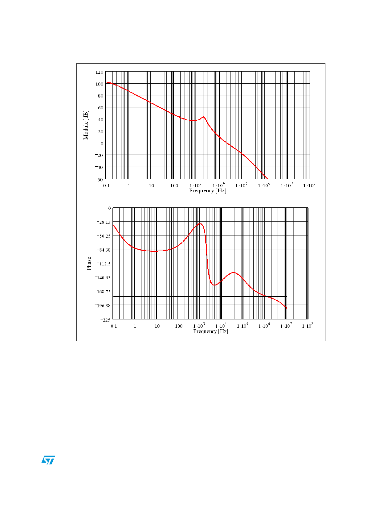
For example with V
=5 V, VIN=24 V, IO=3 A, L=18 µH, C
OUT
=330 µF, ESR=35 mΩ, the
OUT
type II compensation network is:
R
1.1k Ω= R2150Ω= R44.99k Ω= C482nF= C568pF=,, ,,
1
In Figure 15 the module and phase of the open-loop gain is shown. The bandwidth is about
21 kHz and the phase margin is 45°.
26/44 Doc ID 022450 Rev 2
Page 27
L7986 Application information
Figure 15. Open-loop gain Bode diagram with electrolytic/tantalum output capacitor
Doc ID 022450 Rev 2 27/44
Page 28

Application information L7986
6.5 Thermal considerations
The thermal design is important to prevent the thermal shutdown of device if junction
temperature goes above 150 °C. The three different sources of losses within the device are:
a) conduction losses due to the non-negligible R
equal to:
Equation 32
of the power switch; these are
DSON
P
ONRDSONIOUT
where D is the duty cycle of the application and the maximum R
220 mΩ. Note that the duty cycle is theoretically given by the ratio between V
()2D⋅⋅=
overtemperature is
DSON
OUT
and VIN,
but actually it is quite higher to compensate the losses of the regulator. So the conduction
losses increase compared with the ideal case.
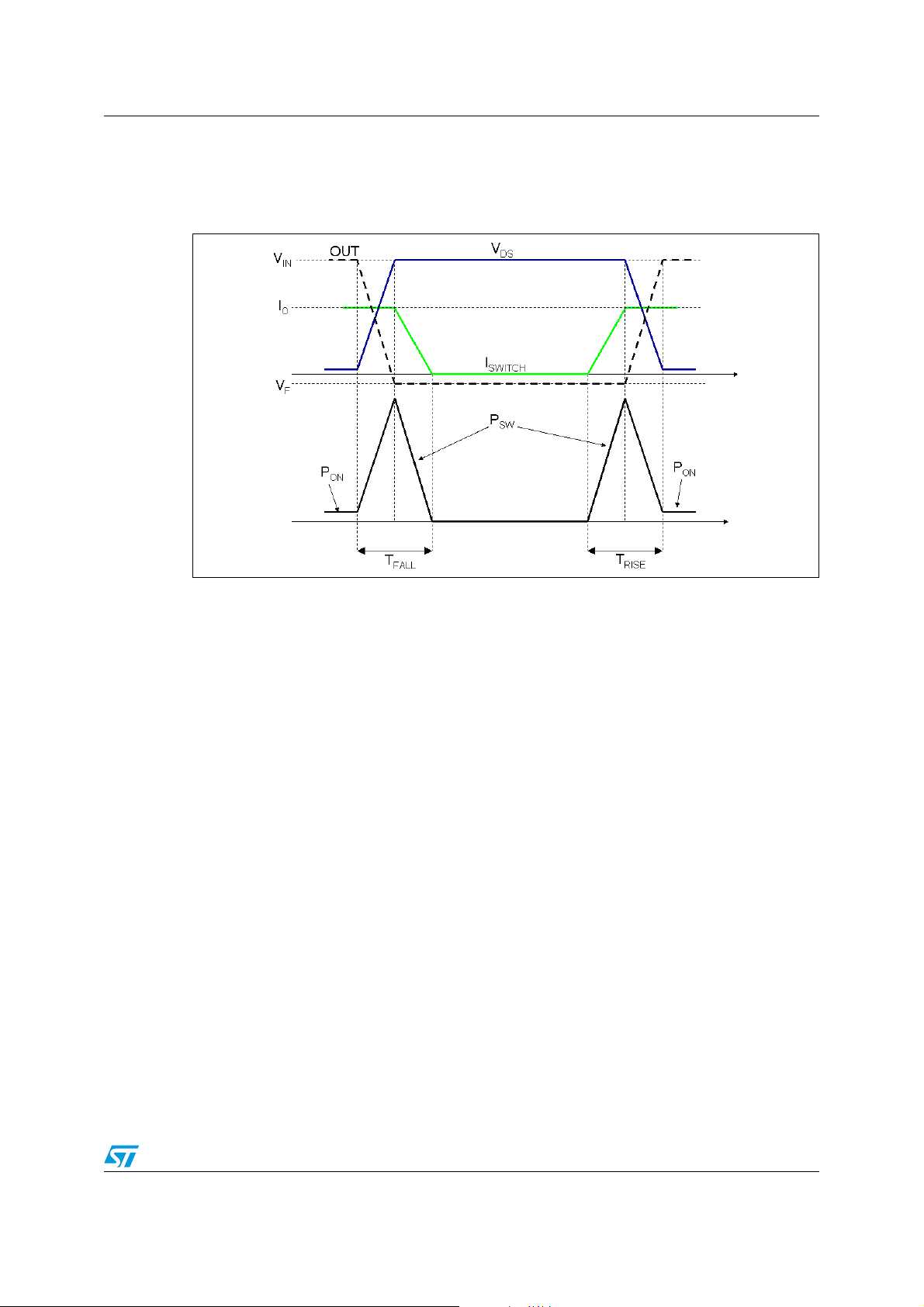
b) switching losses due to power MOSFET turn ON and OFF; these can be
calculated as:
Equation 33
T
+()
RISETFALL
where T
RISE
P
SWVINIOUT
and T
FALL
----------------------------------------------
2
Fsw⋅⋅ ⋅ V
are the overlap times of the voltage across the power switch (VDS)
⋅⋅⋅==
INIOUTTSWFSW
and the current flowing into it during turn ON and turn OFF phases, as shown in Figure 16.
T
is the equivalent switching time. For this device the typical value for the equivalent
SW
switching time is 40 ns.
c) Quiescent current losses, calculated as:
Equation 34
P
QVINIQ
where I
The junction temperature T
is the quiescent current (IQ=2.4 mA).
Q
can be calculated as:
J
Equation 35
T
JTA
where T
Rth
is the ambient temperature and P
A
is the equivalent thermal resistance junction to ambient of the device; it can be
JA
RthJAP
is the sum of the power losses just seen.
TOT
calculated as the parallel of many paths of heat conduction from the junction to the ambient.
For this device the path through the exposed pad is the one conducting the largest amount
28/44 Doc ID 022450 Rev 2
⋅=
⋅+=
TOT
Page 29
L7986 Application information
of heat. The RthJA, measured on the demonstration board described in the following
paragraph, is about 60 °C/W for the VFQFPN package and about 40 °C/W for the HSOP
package.
Figure 16. Switching losses
6.6 Layout considerations
The PC board layout of the switching the DC/DC regulator is very important to minimize the
noise injected in high impedance nodes and interference generated by the high switching
current loops.
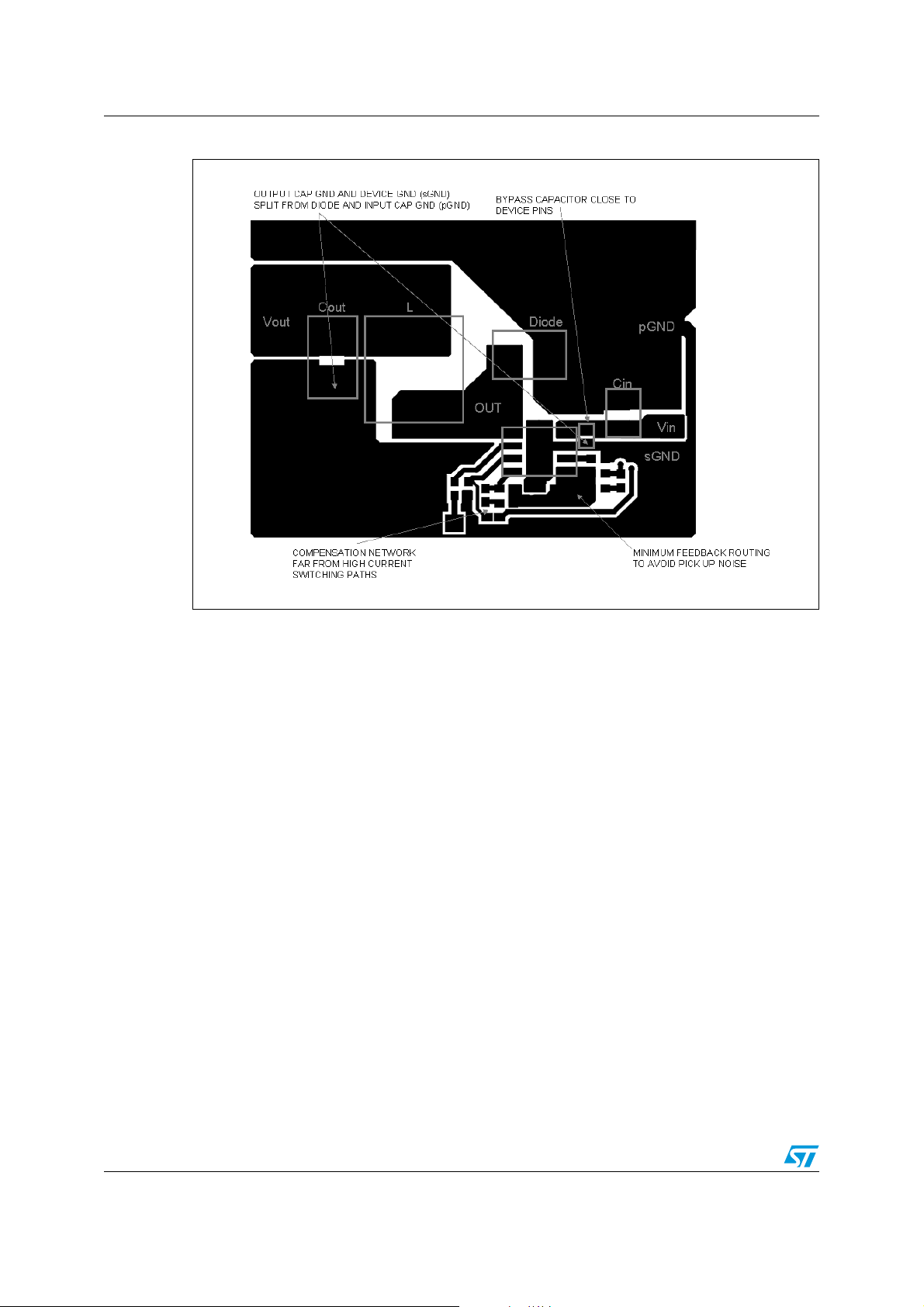
In a step-down converter the input loop (including the input capacitor, the power MOSFET
and the freewheeling diode) is the most critical one. This is due to the fact that the high
value pulsed currents are flowing through it. In order to minimize the EMI, this loop must be
as short as possible.
The feedback pin (FB) connection to the external resistor divider is a high impedance node,
so the interference can be minimized by placing the routing of the feedback node as far as
possible from the high current paths. To reduce the pick-up noise, the resistor divider must
be placed very close to the device.
To filter the high frequency noise, a small bypass capacitor (220 nF - 1 µF) can be added as
close as possible to the input voltage pin of the device.
Thanks to the exposed pad of the device, the ground plane helps to reduce the thermal
resistance junction to ambient; so a large ground plane enhances the thermal performance
of the converter allowing high power conversion.
In Figure 17 a layout example is shown.
Doc ID 022450 Rev 2 29/44
Page 30
Application information L7986
Figure 17. Layout example
30/44 Doc ID 022450 Rev 2
Page 31
L7986 Application information
6.7 Application circuit
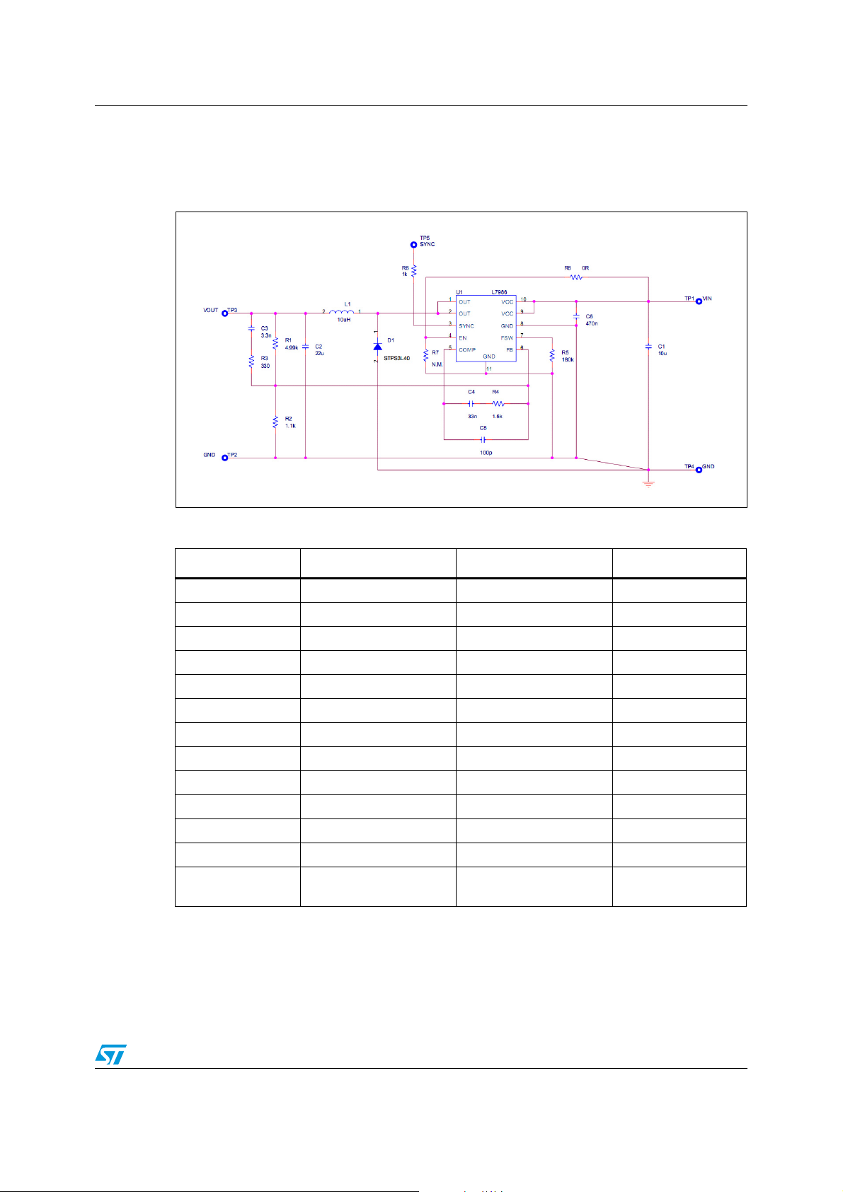
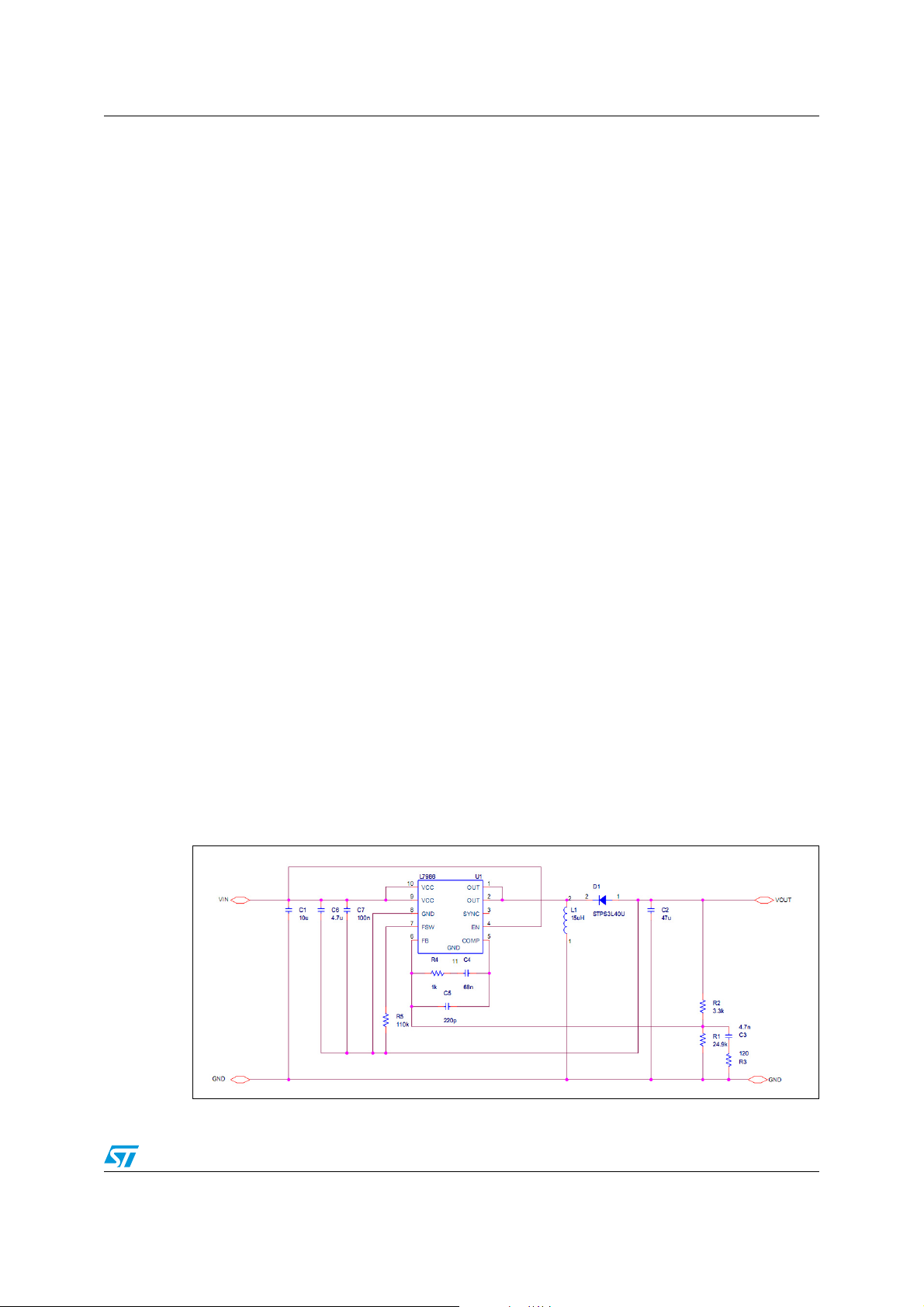
In Figure 18 the demonstration board application circuit is shown.
Figure 18. Demonstration board application circuit
Table 9. Component list
Reference Part number Description Manufacturer
C1 UMK325BJ106MM-T 10 µF, 50V Taiyo Yuden
C2 GRM32ER61E226KE15 22 µF, 25V Murata
C3 3.3 nF, 50V
C4 33 nF, 50V
C5 100 pF, 50V
C6 470 nF, 50V
R1 4.99 kΩ, 1%, 0.1 W 0603
R2 1.1 kΩ, 1%, 0.1 W 0603
R3 330 Ω, 1%, 0.1 W 0603
R4 1.5 kΩ, 1%, 0.1 W 0603
R5 180 kΩ, 1%, 0.1 W 0603
D1 STPS3L40 3A DC, 40 V STMicroelectronics
L1 MSS1038-103NL
10 µH, 30%, 3.9A,
DCR
MAX
=35 mΩ
Coilcraft
Doc ID 022450 Rev 2 31/44
Page 32
Application information L7986
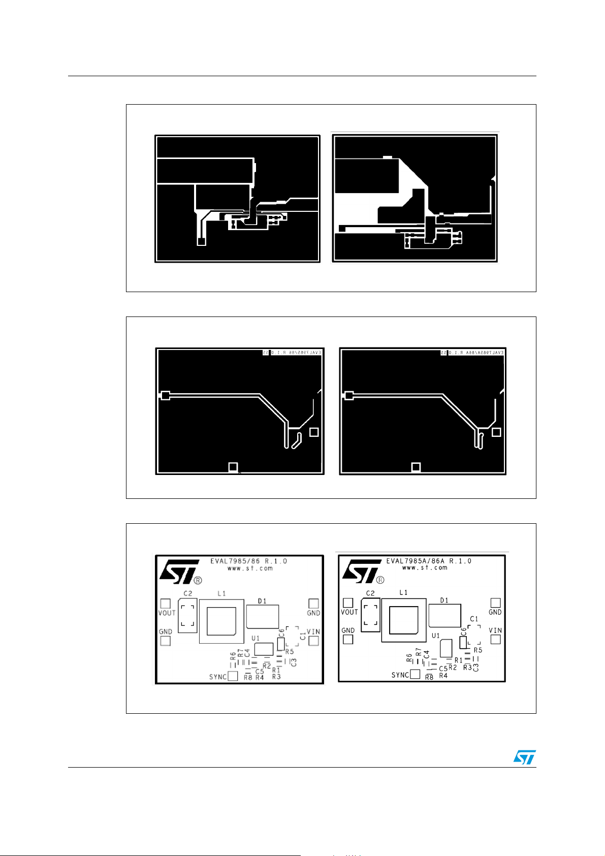
Figure 19. PCB layout: L7986 and L7986A (component side)
Figure 20. PCB layout: L7986 and L7986A (bottom side)
Figure 21. PCB layout: L7986 and L7986A (front side)
32/44 Doc ID 022450 Rev 2
Page 33
L7986 Application information
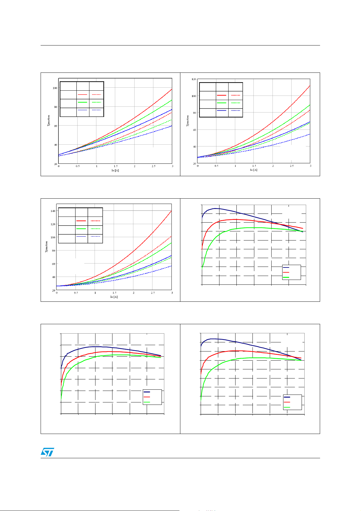
Figure 22. Junction temperature vs. output
V
=5V
OUT
V
=3.3V
OUT
V
=1.8V
OUT
current V
= 24 V
IN
HSOPVQ FN
VIN=24V
F
=250KHz
SW
T
=25 C
AMB
Figure 24. Junction temperature vs. output
V
=3.3V
OUT
V
=1.8V
OUT
V
=1.2V
OUT
VIN=5V
=250KHz
F
SW
T
AMB
current V
=25 C
= 5 V
IN
HSOPVQFN
Figure 23. Junction temperature vs. output
current VIN = 12 V
HSOPVQFN
V
=5V
OUT
V
=3.3V
OUT
V
=1.8V
OUT
VIN=12V
=250KHz
F
SW
=25 C
T
AMB
Figure 25. Efficiency vs. output current
VO = 1.8 V
85
80
75
70
65
60
Eff [ %]
55
50
45
40
0.100 0.600 1.100 1.600 2.100 2.600 3.100
Io [A]
Vo=1.8V
FSW =250kHz
Vin=5V
Vin=12V
Vin=24V
Figure 26. Efficiency vs.output current
V
= 5.0 V
95
90
85
80
Eff [%]
75
70
65
60
0.100 0.600 1.100 1. 600 2.100 2.600 3.100
O
Vo=5.0V
FSW =250kHz
Vin=12 V
Vin=18 V
Vin=24 V
Io [A]
Doc ID 022450 Rev 2 33/44
Figure 27. Efficiency vs.output current
VO = 3.3 V
95
90
85
80
75
Eff [%]
70
65
60
55
50
0.100 0.600 1.100 1.600 2.100 2.600 3.100
Io [A]
Vo=3.3V
FSW =250kHz
Vin= 5V
Vin= 12V
Vin= 24V
Page 34
Application information L7986
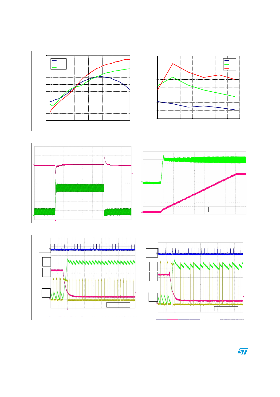
Figure 28. Load regulation Figure 29. Line regulation
3.350
3.345
3.340
3.335
3.330
[V]
OUT
3.325
V
3.320
3.315
3.310
3.305
Figure 30. Load transient: from 0.4 A to 2 A Figure 31. Soft-start
V
OUT
200mV/div
Vin=5V
Vin=12V
Vin=24V
0.00 0.50 1 .00 1.50 2.00 2.50 3.00
Io [A]
3.3600
3.3550
3.3500
3.3450
[V]
3.3400
OUT
V
3.3350
3.3300
3.3250
3.3200
5.0 10.0 15.0 20. 0 25.0 30.0 35.0 40.0
IL1A/div
IL0.5A/div
IL1A/div
IL0.5A/div
VIN[V]
AC coupled
V
V
V
V
OUT
OUT
OUT
OUT
Io= 1A
Io= 2A
Io= 3A
1V/div
0.5V/div
1V/div
0.5V/div
V
=24V
IN
=3.3V
V
OUT
=47uF
C
OUT
1A/div
I
L
L=10uH
=520k
F
SW
Time base 200us/div
OUT
OUT
I
I
L
L
=12 V Figure 33. Short-circuit behavior V
IN
Timebase 10us/div
Timebase 10us/div
Figure 32. Short-circuit behavior V
SYNCH
SYNCH
5V/div
5V/div
OUT
OUT
5V/div
5V/div
V
V
1V/div
1V/div
1A/div
1A/div
SYNCH
SYNCH
SYNCH
SYNCH
5V/div
5V/div
5V/div
5V/div
OUT
OUT
OUT
OUT
5V/div
5V/div
5V/div
5V/div
V
V
V
V
OUT
OUT
OUT
OUT
1V/div
1V/div
1V/div
1V/div
1A/div
1A/div
1A/div
1A/div
Time base 1ms/div
Time base 1ms/div
Time base 1ms/div
Time base 1ms/div
= 24 V
IN
I
I
I
I
L
L
L
L
Timebase 10us/div
Timebase 10us/div
34/44 Doc ID 022450 Rev 2
Page 35
L7986 Application ideas
7 Application ideas
7.1 Positive buck-boost
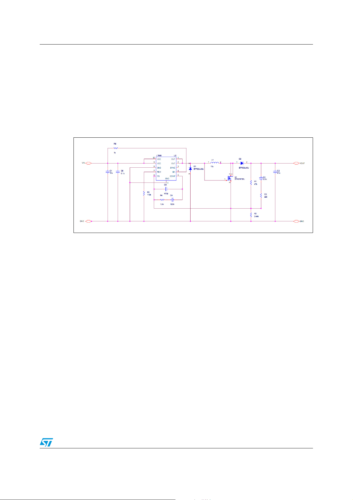
The L7986 can implement the step-up/down converter with a positive output voltage.
Figure 34. shows the schematic: one power MOSFET and one Schottky diode are added to
the standard buck topology to provide 12 V output voltage with input voltage from 4.5 V to 38
V.
Figure 34. Positive buck-boost regulator
The relationship between input and output voltage is:
Equation 36
D
-------------
V
OUTVIN
⋅=
1D–
so the duty cycle is:
Equation 37
V
D
OUT
--------------------------------=
V
+
OUTVIN
The output voltage isn’t limited by the maximum operating voltage of the device (38 V),
because the output voltage is sensed only through the resistor divider. The external power
MOSFET maximum drain to the source voltage, must be higher than the output voltage; the
maximum gate to source voltage must be higher than the input voltage (in Figure 34., if V
IN
is higher than 16 V, the gate must be protected through the Zener diode and resistor).
The current flowing through the internal power MOSFET is transferred to the load only
during the off-time, so according to the maximum DC switch current (3.0 A), the maximum
output current for the buck-boost topology can be calculated from the following equation.
Doc ID 022450 Rev 2 35/44
Page 36
Application ideas L7986
Equation 38
I
OUT
-------------
1D–
3 A<=
I
SW
where I
is the average current in the embedded power MOSFET in the on-time.
SW
To chose the right value of the inductor and to manage transient output current, that for a
short time can exceed the maximum output current calculated by Equation 38, also the peak
current in the power MOSFET must be calculated. The peak current, shown in Equation 39,
must be lower than the minimum current limit (3.7 A).
Equation 39
I
SW,PK
--------------------------------------------
r
I
OUT
OUT
-------------
1D–
V
OUT
LF
⋅⋅
1
SW
r
-- -+ 3.7 A<⋅=
2
⋅=
1D–()
2
I
where r is defined as the ratio between the inductor current ripple and the inductor DC
current:
So, in the buck-boost topology the maximum output current depends on the application
conditions (firstly input and output voltage, secondly switching frequency and inductor
value).
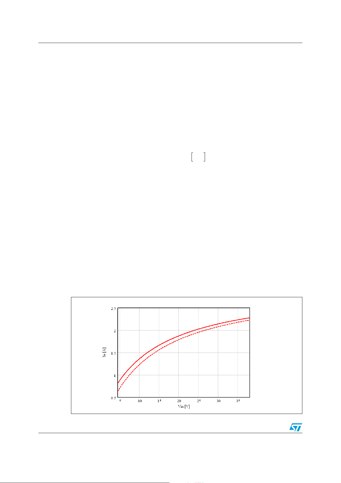
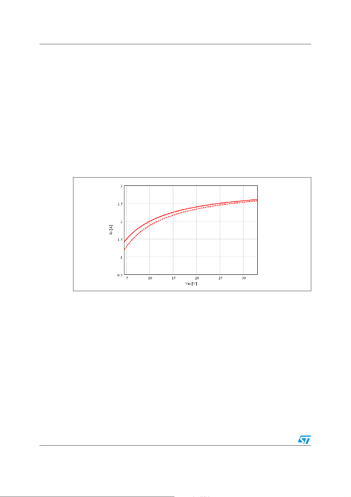
In Figure 35. the maximum output current for the above configuration is depicted varying the
input voltage from 4.5 V to 38 V.
The dashed line considers a more accurate estimation of the duty cycles given by Equation
40, where power losses across diodes, external power MOSFET, and internal power
MOSFET are taken into account.
Figure 35. Maximum output current according to max DC switch current (3.0 A):
V
=12 V
O
36/44 Doc ID 022450 Rev 2
Page 37
L7986 Application ideas
Equation 40
V
2V
D
-------------------------------------------------------------- -------------------------------------=
V
INVSWVSWEVOUT
OUT
⋅+
D
++––
2V⋅
D
where V
is the voltage drop across the diodes, VSW and V
D
external power MOSFET.
7.2 Inverting buck-boost
The L7986 can implement the step-up/down converter with a negative output voltage.
Figure 34. shows the schematic to regulate -5 V: no further external components are added
to the standard buck topology.
The relationship between input and output voltage is:
Equation 41
so the duty cycle is:
Equation 42
V
OUT
D
VIN–
V
OUT
------------------------------- -=
V
–
OUTVIN
⋅=
D
-------------
1D–
across the internal and
SWE
As in the positive one, in the inverting buck-boost the current flowing through the power
MOSFET is transferred to the load only during the off-time. So according to the maximum
DC switch current (3.0 A), the maximum output current can be calculated from Equation 38,
where the duty cycle is given by Equation 42.
Figure 36. Inverting buck-boost regulator
Doc ID 022450 Rev 2 37/44
Page 38
Application ideas L7986
The GND pin of the device is connected to the output voltage so, given the output voltage,
the input voltage range is limited by the maximum voltage the device can withstand across
VCC and GND (38 V). Therefore, if the output is -5 V the input voltage can range from 4.5 V
to 33 V.
As in the positive buck-boost, the maximum output current according to application
conditions is shown in Figure 37. The dashed line considers a more accurate estimation of
the duty cycles given by Equation 43, where power losses across diodes and the internal
power MOSFET are taken into account.
Equation 43
V
–
------------------------------------------------------ --------------=
D
OUTVD
V–
INVSWVOUTVD
–+–
Figure 37. Maximum output current according to switch max. peak current (3.0 A):
V
= - 5 V
O
38/44 Doc ID 022450 Rev 2
Page 39

L7986 Package mechanical data
8 Package mechanical data
In order to meet environmental requirements, ST offers these devices in different grades of
ECOPACK
specifications, grade definitions and product status are available at: www.st.com.
ECOPACK
®
packages, depending on their level of environmental compliance. ECOPACK®
®
is an ST trademark.
Doc ID 022450 Rev 2 39/44
Page 40
Package mechanical data L7986
7
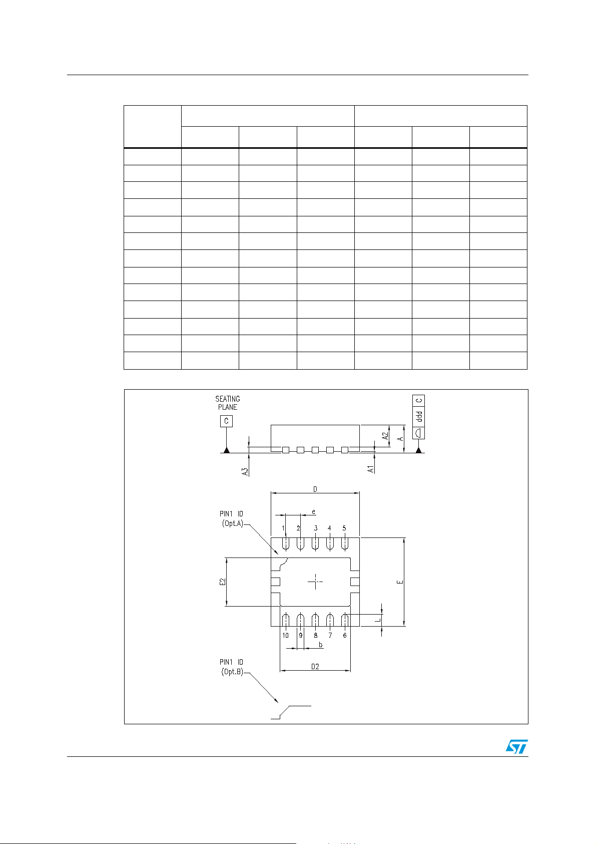
Table 10. VFQFPN10 (3x3x1.08mm) mechanical data
mm inch
Dim.
Min. Typ. Max. Min. Typ. Max.
A 0.80 0.90 1.00 0.0315 0.0354 0.0394
A1 0.02 0.05 0.0008 0.0020
A2 0.70 0.0276
A3 0.20 0.0079
b 0.18 0.23 0.30 0.0071 0.0091 0.0118
D 2.95 3.00 3.05 0.1161 0.1181 0.1200
D2 2.21 2.26 2.31 0.087 0.089 0.0906
E 2.95 3.00 3.05 0.1161 0.1181 0.1200
E2 1.49 1.64 1.74 0.0587 0.0646 0.0685
e 0.50 0.0197
L 0.3 0.40 0.5 0.0118 0.0157 0.0197
M 0.75 0.0295
m 0.25 0.0098
Figure 38. VFQFPN10 (3x3x1.08mm) package dimensions
40/44 Doc ID 022450 Rev 2
Page 41
L7986 Package mechanical data
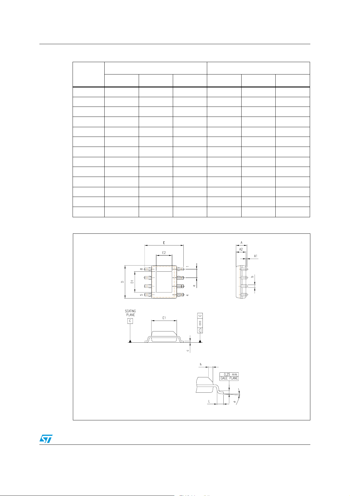
Table 11. HSOP8 mechanical data
mm inch
Dim
Min. Typ. Max. Min. Typ. Max.
A 1.70 0.0669
A1 0.00 0.150 0.00 0.0059
A2 1.25 0.0492
b 0.31 0.51 0.0122 0.0201
c 0.17 0.25 0.0067 0.0098
D 4.80 4.90 5.00 0.1890 0.1929 0.1969
E 5.80 6.00 6.20 0.2283 0.2362 0.2441
E1 3.80 3.90 4.00 0.1496 0.1535 0.1575
e 1.27 0.0500
h 0.25 0.50 0.0098 0.0197
L 0.40 1.27 0.0157 0.0500
k 0.00 8.00 0.3150
ccc 0.10 0.0039
Figure 39. HSOP8 package dimensions
$MM4YP
%MM4YP
!-V
Doc ID 022450 Rev 2 41/44
Page 42

Order codes L7986
9 Order codes
Table 12. Order codes
Order codes Package Packaging
L7986 VFQFPN10 Tube
L7986A HSOP8 Tube
L7986TR VFQFPN10 Tape and reel
42/44 Doc ID 022450 Rev 2
Page 43

L7986 Revision history
10 Revision history
Table 13. Document revision history
Date Revision Changes
07-Nov-2011 1 Initial release.
01-Mar-2012 2 Section 8: Package mechanical data has been updated.
Doc ID 022450 Rev 2 43/44
Page 44

L7986
Please Read Carefully:
Information in this document is provided solely in connection with ST products. STMicroelectronics NV and its subsidiaries (“ST”) reserve the
right to make changes, corrections, modifications or improvements, to this document, and the products and services described herein at any
time, without notice.
All ST products are sold pursuant to ST’s terms and conditions of sale.
Purchasers are solely responsible for the choice, selection and use of the ST products and services described herein, and ST assumes no
liability whatsoever relating to the choice, selection or use of the ST products and services described herein.
No license, express or implied, by estoppel or otherwise, to any intellectual property rights is granted under this document. If any part of this
document refers to any third party products or services it shall not be deemed a license grant by ST for the use of such third party products
or services, or any intellectual property contained therein or considered as a warranty covering the use in any manner whatsoever of such
third party products or services or any intellectual property contained therein.
UNLESS OTHERWISE SET FORTH IN ST’S TERMS AND CONDITIONS OF SALE ST DISCLAIMS ANY EXPRESS OR IMPLIED
WARRANTY WITH RESPECT TO THE USE AND/OR SALE OF ST PRODUCTS INCLUDING WITHOUT LIMITATION IMPLIED
WARRANTIES OF MERCHANTABILITY, FITNESS FOR A PARTICULAR PURPOSE (AND THEIR EQUIVALENTS UNDER THE LAWS
OF ANY JURISDICTION), OR INFRINGEMENT OF ANY PATENT, COPYRIGHT OR OTHER INTELLECTUAL PROPERTY RIGHT.
UNLESS EXPRESSLY APPROVED IN WRITING BY TWO AUTHORIZED ST REPRESENTATIVES, ST PRODUCTS ARE NOT
RECOMMENDED, AUTHORIZED OR WARRANTED FOR USE IN MILITARY, AIR CRAFT, SPACE, LIFE SAVING, OR LIFE SUSTAINING
APPLICATIONS, NOR IN PRODUCTS OR SYSTEMS WHERE FAILURE OR MALFUNCTION MAY RESULT IN PERSONAL INJURY,
DEATH, OR SEVERE PROPERTY OR ENVIRONMENTAL DAMAGE. ST PRODUCTS WHICH ARE NOT SPECIFIED AS "AUTOMOTIVE
GRADE" MAY ONLY BE USED IN AUTOMOTIVE APPLICATIONS AT USER’S OWN RISK.
Resale of ST products with provisions different from the statements and/or technical features set forth in this document shall immediately void
any warranty granted by ST for the ST product or service described herein and shall not create or extend in any manner whatsoever, any
liability of ST.
ST and the ST logo are trademarks or registered trademarks of ST in various countries.
Information in this document supersedes and replaces all information previously supplied.
The ST logo is a registered trademark of STMicroelectronics. All other names are the property of their respective owners.
© 2012 STMicroelectronics - All rights reserved
STMicroelectronics group of companies
Australia - Belgium - Brazil - Canada - China - Czech Republic - Finland - France - Germany - Hong Kong - India - Israel - Italy - Japan -
Malaysia - Malta - Morocco - Philippines - Singapore - Spain - Sweden - Switzerland - United Kingdom - United States of America
www.st.com
44/44 Doc ID 022450 Rev 2
 Loading...