

Page 1
L6920
1V HIGH EFFICIENCY SYNCRONO US STEP UP CONVERTER
■ 0.6 TO 5.5V OPERATING IN PUT VOLTA GE
■ 1V START UP INPUT VOLTAGE
■ INTERNAL SYNCHRONOUS RECTIFIER
■ ZERO SHUT DOWN CURRENT
■ 3.3V AND 5V FIXED OR ADJUSTABLE
OUTPUT VOLTAGE (2V UP TO 5.2V)
■ 120mΩ INTERNAL ACTIVE SWITCH
■ LOW BATTERY VOLTAGE DETECTION
■ REVERSE BATTERY PROTECTION
ORDERING NUMBER: L6920D
TSSOP8
Applications
■ ONE TO THREE CELL BATTERY DEVICES
■ PDA AND HAND HELD INSTRUMENTS
■ CELLULAR PHONES - DIGITAL CORDLESS
PHONE
■ PAGERS
■ GPS
■ DIGITAL CAMERAS
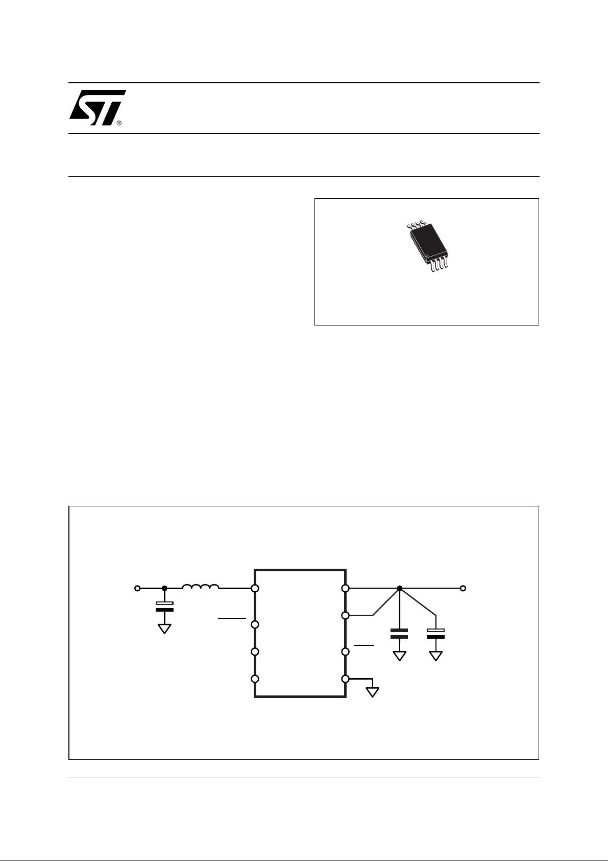
APPLICATION CIRCUIT
L1
V
CC
2.5V 3.3V
C2
LX
SHDN
7
5
L6920
DESCRIPTION
The L6920 is a high efficiency step-up controller requiring only three external components to realize the
conversion from the battery voltage to the selected
output voltage.
The start up is guaranteed at 1V and the dev ice is operating down to 0.6V.
Internal synchronous rectifier is implemented with a
120m
Ω
P-channel MOSFET and, in order to i mpr ove
the efficiency, a variable frequency control is implemented.
OUT
8
V
OUT
FB
1
500mA
C3 C1
May 2003
LBI
REF
2
3
LBO
GND
4
6
D00IN1136C
1/12
Page 2
L6920
8
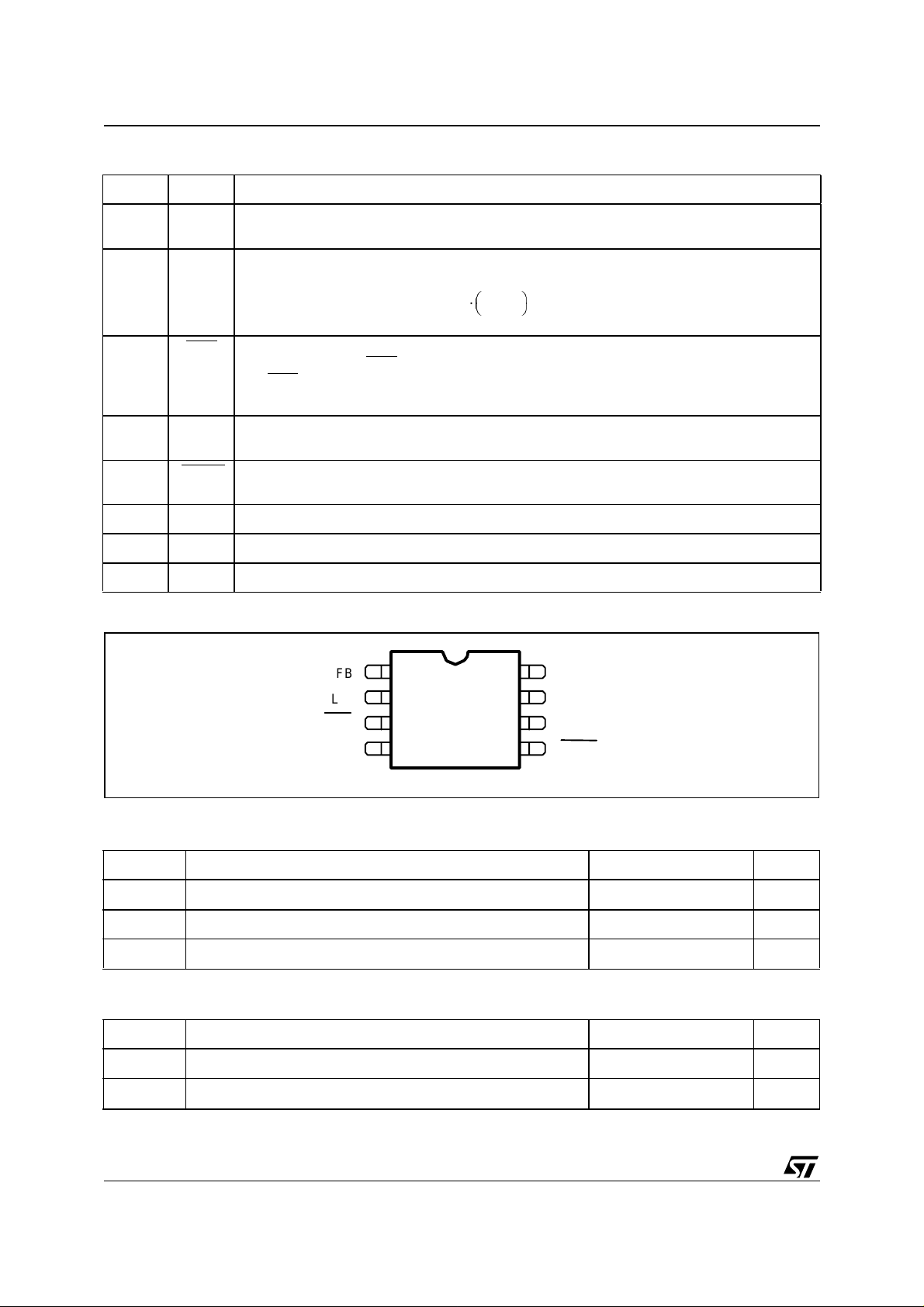
PIN DESCRIPTION
Pin Name Function
1FB
Output voltage selector. Connect FB to GND for Vout=5V or to OUT for Vout=3.3V. Connect FB to an
external resistor divider for adjustable output voltage (from 2V to 5.2V) [see R4 and R5, fig. 7].
2 LBI Battery low voltage detector input. The internal threshold is set to 1.23V.
A resistor divider is needed to adjust the desired low battery threshold:
R1
V
1.23V= 1
LBI
3
LBO
Battery low voltage detector output. If the voltage at the LBI pin drops below the internal
------- -+
⋅
[see R1 and R2, fig. 7]
R2
threshold typ. 1.23V, LBO goes low.
LBO is an open drain output and so a pull-up resistor (about 200KΩ) has to be added for
The
correct output setting [see R3, fig. 7].
4 REF 1.23V reference voltage. Bypass this output to GND with a 100nF capacitor for filtering high
frequency noise. No capacitor is required for stability
5
SHDN
Shutdown pin. When pin 5 is below 0.2V the device is in shutdown, when pin 5 is above 0.6V the
device is operating.
6 GND Ground pin
7 LX Step-up inductor connection
8 OUT Power OUTPUT pin
PIN CONNECTION (Top vi ew)
FB
LBI
LBO
REF
8
2
3
4
TSSOP
7
6
5
OUT1
LX
GND
SHDN
ABSOLUTE MAXIMUM RATINGS
Symbol Parameter Value Unit
V
ccmax
Vcc to GND 6 V
LBI, SHDN, FB to GND 6 V
V
out max
Vout to GND 6 V
THERMAL DATA
Symbol Parameter Value Unit
R
th j-amb
T
Thermal Resistance Junction to Ambient 250 °C/W
Maximum Junction Temperature 150 °C
j
2/12
Page 3
L6920
ELECTRICAL CHARACTERISTCS
(Vin = 2V, FB = GND, T
= -40°C to 85°C and Tj < 125°C unless other-
amb
wise specified))
Symbol Parameter Test Condition Min. Typ. Max. Unit
SECTION
V
CC
in
in
I
q
I
sd
on-N
on-P
Minimum operating Input Voltage 0.6 V
Minimum Start Up Input Voltage 1 V
Quiescent Current Il =0 mA, FB = 1.4V, V
LBI = SHDN = 2V, Tj = T
I
=0 mA, FB = 1.4V, V
l
LBI = SHDN = 2V, Tj = T
= 3.3V
out
amb
= 5V
out
amb
915µA
11 18 µA
Shut Down Current Vin = 5V, Il =0 mA 0.1 5 µA
amb
0.1 2 µA
Active switch ON resistance 120 250 mΩ
Synchronous switch ON
120 250 mΩ
resistance
V
V
Irev Reverse battery current Vin = -4V, Tj = T
POWER SECTION
R
R
CONTROL SECTION
Vout Output voltage FB = OUT, Il =0 mA 3.2 3.3 3.4 V
FB = GND, Il =0 mA 4.9 5 5.1 V
Output voltage range External divider 2 5.2 V
V
V
I
T
onmax
T
offmin
SHDN SHDN logic LOW
V
LBI threshold 1.18 1.23 1.27 V
LBI
0°C < T
LBO logic LOW
LBO
LX switch current limit 0.8 1 1.2 A
lim
I
Maximum on time V
Minimum off time V
SHDN logic HIGH
Reference Voltage 1.18 1.23 1.27 V
ref
< 70°C 1.205 1.23 1.255 V
j
< 250µA 0.2 0.4 V
sink
= 2V to 5.3V 3.75 5 6.25 µs
out
= 2V to 5.3V 0.75 1 1.25 µs
out
0.6 V
0.2 V
3/12
Page 4
L6920
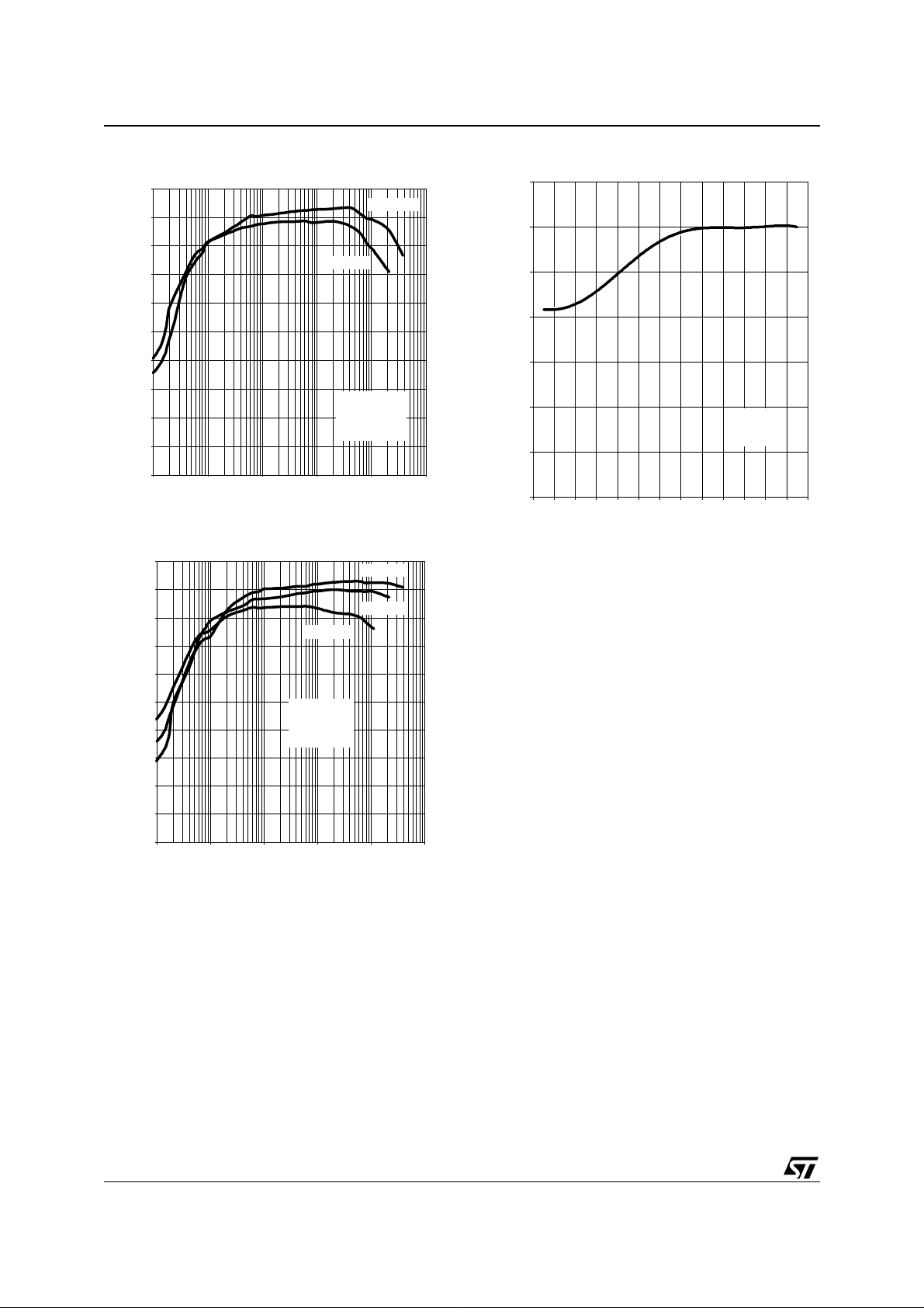
Figure 1.
Efficiency vs. Output Current
100
90
80
Vin = 1.2V
70
60
]
]
]
]
%
%
%
%
[
[
[
[
η
η
η
η
50
EFFICIENCY
40
30
20
10
0
0.01 0.1 1 10 100 1000
Figure 2.
Efficiency vs. Output Current
100
90
80
LOAD CURRENT [mA]
Vout = 3. 3V
L = 47µH
C = 100µF
Vin = 1.2V
70
Vin = 2.4V
Vin = 3.6V
Vin = 2.4V
Fig u re 3. Startup Vol tage v s Outpu t Curr ent
1.4
1.2
1
0.8
0.6
Startup voltage (V)
0.4
0.2
0
30 60 90 120 150 180
Output current (mA)
L = 47µH
C = 22µF
60
]
]
]
]
%
%
%
%
[
[
50
[
[
η
η
η
η
EFFICIENCY
40
30
20
10
0
0.01 0.1 1 10 100 1000
f
Vout = 5V
L = 47µH
C = 100µF
LOAD CURRENT [mA]
4/12
Page 5

L6920
DETAILED DESCRIPTION
The L6920 is a high efficiency, low voltage step- up DC/DC conve rter partic ular ly su itable for 1 to 3 cell s (L i-Ion/
polymer, NiMH respectively) battery up conversion.
µ
These performances are achieved via a strong reduction of quiescent current (10
chronous rectification, that implies also a reduced cost in the application (no external diode required).
Operation is based on maximum ON time - minimum OFF time control, tailored by a current limit set to 1A. A
simplified block diagram is shown here below.
Figure 4. Simplified Block Diagram
A only) and adopting a syn-
V
REF
SHDN
LBO
OUT
LBI
A
B
C
(CR)
ZERO CROSSING
RQS
+
VBG
FB Y
V
OUT
GND
R1,R
Y
VBG
2
-
+
Toff min
1µsec
VBG
OPAMP
A
B
C
+
Ton max
5µsec
-
- +
+
CURRENT LIMIT
VOUT
LX
+
GND
FB
D99IN1041
V
OUT
V
IN
PRINCIPLE OF OPERATION
In L6920 the control is based on a comparator that continuously checks the status of output voltage.
If the output voltage is lower than the expected value, t he control function of the L6920 directs the energy stor ed
in the inductor to be transferred to the load. This is accomplished by alternating between two basic steps:
- TON phase: the energy is transfer red from the battery to the inductor by shor ting LX node to gr ound via the Nchannel power switch. The switch is turned off i f the curre nt flowing in the inductor r eaches 1A or after a maximum on time set to 5
µ
s.
- TOFF phase: the energy stored in the inductor is tr ansferred to the load thr ough the synchronous swi tch for at
least a minimum off time equal to 1
µ
s. After this, the synchronous switch is turned off as soon as the output
voltage goes lower than the regulated voltage or the current flowing in the inductor goes down to zero.
So, in case of light load, the device works in PFM mode, as shown in figure 5.
5/12
Page 6

L6920
Figure 5.1.
Figure 5.2.
PFM mode Condition: V
= 5V; Vin
out
=1.5V. Trace1: Vout (50mV~/div) Trace
4: IL (100mA/div) Time div.: 5µs/div
Heavier load - Train pulses overlapping.
Trace1: V
(100mV~/div) Trace 4: IL
out
(200mA /div) T ime div.: 10 µs/div
Figure 5.3.
Figure 5.4.
Heavy load - Inductor current ripples
below I
Trace1: V
lim
(100mV~/div)
out
Trace 4: IL (200mA/div) Time di v. : 20 µs/div
Heavy load and High ESR. Regulation
falls in continuous mode of operation.
Trace1: V
(100mV~/div) Trace 4: IL
out
(200mA/div). Time div.: 5 µs/div
When Iload is heavier, the pulse trains are overlapped. Figures 5.2 - 5.4 show some possible behaviors.
Considering that current in the inductor is limited to 1A, the maximum load current is defined by the following
relationship:
Where
η
is the efficiency and I
I
load _lim
lim
=1A.
V
in
-----------
V
I
–
limToff min
out
–
V
outVin
------------------------- -
⋅
2L⋅
eq. (1)
η⋅⋅=
Of course, if Iload is greater than Iload_lim the regulation is lost (figure 6).
6/12
Page 7

L6920
Figure 6. No regulation. I
V
(100mV~/div) Trace 4: IL (200mA/div).
out
load
> I
load_lim
Trace1:
Time div.: 5 µ s/div
Start-up
One of the key features of L6920 is the startup at supply voltage down to 1V (please see the diagram in
Figure 3. in case of heavy load).
The device leaves the startup mode of operation as
soon as VOUT goes over 1.4V. During startup, the
synchronous switch is off and the energy is transferred to the load through its intrinsic body diode.
The N-channel switches with a very low RDSon
thanks to an internal charge pump used to bias the
power mos gate. Because of this modified behavior,
TON/TOFF times are lengthened. Current limit and
zero crossing detection are still available.
The synchronous switch body diode causes a parasitic path between power supply and output that can't
be avoided also in shutdown.
Low battery detection
The L6920 includes a low battery detector comparator. Threshold is VREF voltage and a 1.3% hysteresis is added to avoid oscillations when input crosses
the threshold slowly. The
LBO
is an open drain out-
put so a pull up resistor is required for a proper use.
Reverse polarity
A protection circuit has been implemented to avoid
that L6920 and the battery are destroyed in case of
wrong battery insertion.
In addition, this circuit has been designed so that the
current required by the battery is zero also i n rever se
polarity.
APPLICATION INFORMATION
Output voltage selection
Output voltage must be selected acting on FB pin.
Three choices are av ailable : fixed 3.3V , 5V or a djustable output set via an external resistor divider.
OUTPUT VOLTAGE SELECTION
V
= 3.3V FB pin connected to OUT (see
OUT
= 5V FB pin connected to GND
V
OUT
application circui t)
Shutdown
In shutdown mode (
SHDN
pulled low) all internal circuitries are turned off, minimizing the current provided by the battery (I
< 100 nA, in typical case).
SHDN
Both switches are turned off, and the low battery
comparator output is forced in high impedance state.
2V ≤ V
≤ 5.2V FB pin connected to a resistive
OUT
divider
V
OUT
1.23V 1
=
R4
------- -+
R5
7/12
Page 8

L6920
Figure 7. Dem ob oard Circui t
+VBATT
R1
N.C.
LBI
2
R2
N.C.
VREF
C4
100nF
not mounted components
GND
4
6
VBATT
L6920
F.B.
Panasonic
ELL6RH100M
L1 10µH
7
VOUT
8
R3
N.C.
LBO
3
SHDN
5
1
J1
C3
N.C.
1
2
3
1
2
J2
3
C2
47µF
C1
47µF
R4 N.C.
R5 N.C.
Panasonic
EEFCDJ470R
Panasonic
EEFCDJ470R
D01IN1310
+VBATT
GND
VOUT
GND
LBO
SHDN
Jumper Position Function
1-2 Device enabled
J1
2-3 Device disabled
None Adjustable using R4 and R5 [not
mounted]
J2
1-2 3.3V output voltage
2-3 5V output voltage
R4, R5 should be s elected in the range of 100kΩ - 10MΩ to minimize c onsumption and error due to current s unk
by FB pin (few nA).
Output capacitor selection
The output capacitor affects both efficiency and output ripple so its choice has to be considered with particular
care.
The capacitance value should be in the range of about 10
µ
F-100µF.
An additional, smaller, low ESR capacitor can be in parallel for high frequency filtering. A typical value can be
µ
around 1
F.
If very high performances, in terms of efficiency and output voltage ripple, are required, a very low ESR capacitor has to be chosen.
Ceramic capacitors are the lowest ESR but they are very expensive.
Other possibilities are low-ESR tantalum capacit ors, available fr om KEMET, AVX and other sources. POSCAP
capacitors from SANYO and polymeric capacitors from PANASONIC are also good.
Below there is a l ist of some c apacitors supplier s . The cap values and rated v oltages a re only a suggested pos-
sibility
8/12
Page 9

Table 1. Capacitors distributors main list
Manufacturer Series Cap Value (µF) Rated Voltage (V) ESR (mΩ)
AVX TPS 15 to 470 6.3 50 to 1500
L6920
KEMET T510/T494/
T495
PANASONIC EEFCD 22 to 47 6.3 50 to 700
SANYO POSCAP TPA/B/C 22 to 230 6.3 40 to 80
SPRAGUE 595D 100 to 390 6.3 160 to 700
10 to 470 6 30 to 1000
Inductor selection
Usually, inductors ranging between 5µH to 40µH satisfy most of the applications.
Small value inductors have smaller phy sical size a nd guarantee a faster respons e to load transient but in s teady
state condition a bigger ripple on output voltage is generated. In fact the output ripple voltage is given by Ipeak
multiplied by ESR. Furthermore, as shown in equation (1), inductor size affects also the maximum current deliverable to the load. Lastl y, a low series resistanc e is s uggested if ver y high ef ficienc y values are needed. A nyway, the saturation current of the choke should be higher than the peak current limit of the device (1A).
Good surface mounting i nductors are availabl e fr om COILCRAFTS, COILTRONICS, MURATA and other souces. In the following table are listed some suggested components.
Table 2. Inductors distributors main list
Manufacture r Series Inductor Value (uH) Saturation Current (A)
Coilcraft DO1813HC 22 to 33 1 to 1.2
DO1608 4.7 to 15 0.9 to 1.5
Coiltronics UP1B 22 to 33 1 to 1.2
TP3 4.7 to 15 0.97 to 1.6
BI HM76-2 22 to 33 1 to 1.2
HM76-1 4.7 to 10 1 to 1.5
Murata LQN6C 10 to 22 1.2 to 1.7
Panasonic ELL6SH 10 to 22 0.9 to 1.5
ELL6RH 5.1 to10 11 to 1.55
Sumida CR43 4.7 to 10 0.84 to 1.15
Layout Guidelines
The board layout is very important in order to minimize noise, high frequency resonance problems and electromagnetic interference.
It is essential to keep as small as possible the high switching current circulating paths to reduce radiation and
resonance problems. So, the output and input cap should be very close to the device.
The external resistor dividers, if used, should be as cl ose as possibl e to the pi ns of the dev ice (F B and LBI) and
as far as possible from the high current circulating paths, to avoid pick up noise.
Large traces for high current paths and an extended groundplane, help to reduce the noise and increase the
efficiency.
For an example of recommended layout see the following evaluation board
9/12
Page 10

L6920
Figure 8. Figu re 8. De m o board Comp onents (Top s i de) .
Figure 9. Dem ob oard Layout (Top side).
4.5cm
4cm
Figure 10. Demoboard Layout (Bottom side).
4.5cm
4cm
4.5cm
4cm
10/12
Page 11

L6920
DIM.
mm inch
MIN. TYP. MAX. MIN. TYP. MAX.
A 1.20 0.047
A1 0.050 0.150 0.002 0.006
A2 0.800 1.0 00 1.050 0.031 0.039 0.041
b 0.190 0.300 0.007 0.0 12
c 0.090 0.200 0.003 0.008
D (1) 2.900 3.000 3.100 0.114 0.118 0.122
E 6.200 6.400 6.650 0.244 0.252 0.260
E1 (1) 4.300 4.400 4.500 0.169 0.173 0.177
e 0.650 0.026
L 0.450 0.600 0.750 0.018 0.024 0.027
L1 1.000 0.039
k 0˚ (min.) 8˚ (max.)
aaa 0.100 0.004
Note: 1. D and F doe s not include mold flash o r protru sions.
Mold flash or potrusions shall not exceed 0.15mm
(.006inch) per side.
OUTLINE AND
MECH ANICAL DA T A
TSSOP8
(Body 4.4mm)
0079397 (Jedec MO-153-AA)
11/12
Page 12

L6920
Information furnished is believed to be accurate and reliable. However, STMicroelectronics assumes no responsibility for the consequences
of use of such information nor for any infringement of patents or other rights of third parties which may result from its use. No license is granted
by implic ation or otherwise under any patent or patent ri ghts of STMicroelectronics . S pecificat i ons menti oned in th i s publicati on are subject
to change without notice. This publication supersedes and replaces all information previously supplied. STMicroelectronics products are not
authorized for use as cri tical comp onents in lif e support dev i ces or systems wi thout exp ress written approval of STMicroe l ectronics.
The ST logo is a registered trademark of STMicroelectronics
© 2003 STMic roelectroni cs - All Rig hts Reserved
Austra lia - Brazil - Canada - China - Finland - France - Germany - Hon g K ong - India - Israel - Italy - J apan -Mal aysia - Malta - Morocco -
Singap ore - Spain - Sw eden - Switzerland - Uni ted Kingdom - United St ates.
STMicroelectronics GROUP OF COMPANIES
http://www.s t. com
12/12
 Loading...