

Page 1
查询L6732C供应商
Adjustable Step-Down Controller With Synchronous Rectification
Features
■ INPUT VOLTAGE RANGE FROM 1.8V TO
14V
■ SUPPLY VOLTAGE RANGE FROM 4.5V TO
14V
■ ADJUSTABLE OUTPUT VOL TAGE DOW N
TO 0.6V WITH ±0.8% ACCURACY OVER
LINE VOLTAGE AND TEMPERAT U RE
(0°C~125°C)
■ FIXED FREQUENCY VOLTAGE MODE
CONTROL
■ T
■ 0% TO 100% DUTY CYCLE
■ EXTERNAL INPUT VOLTAGE REFERENCE
■ SOFT-START AND INHI BIT
■ HIGH CURRENT EMBEDDED DRIVERS
■ PREDICTIVE ANTI-CROSS CONDUCTION
■ PROGRAMMABLE HIGH-SIDE AND LOW-
■ SELECTABLE SWITCHING FREQUENCY
■ PRE-BIAS START UP CAPABIL ITY
■ POWER GOOD OUTPUT
■ MASTER/SLAVE SYNCHRONIZATI ON WITH
■ OVER VOLTAGE PROTECTION
■ THERMAL SHUT-DOWN
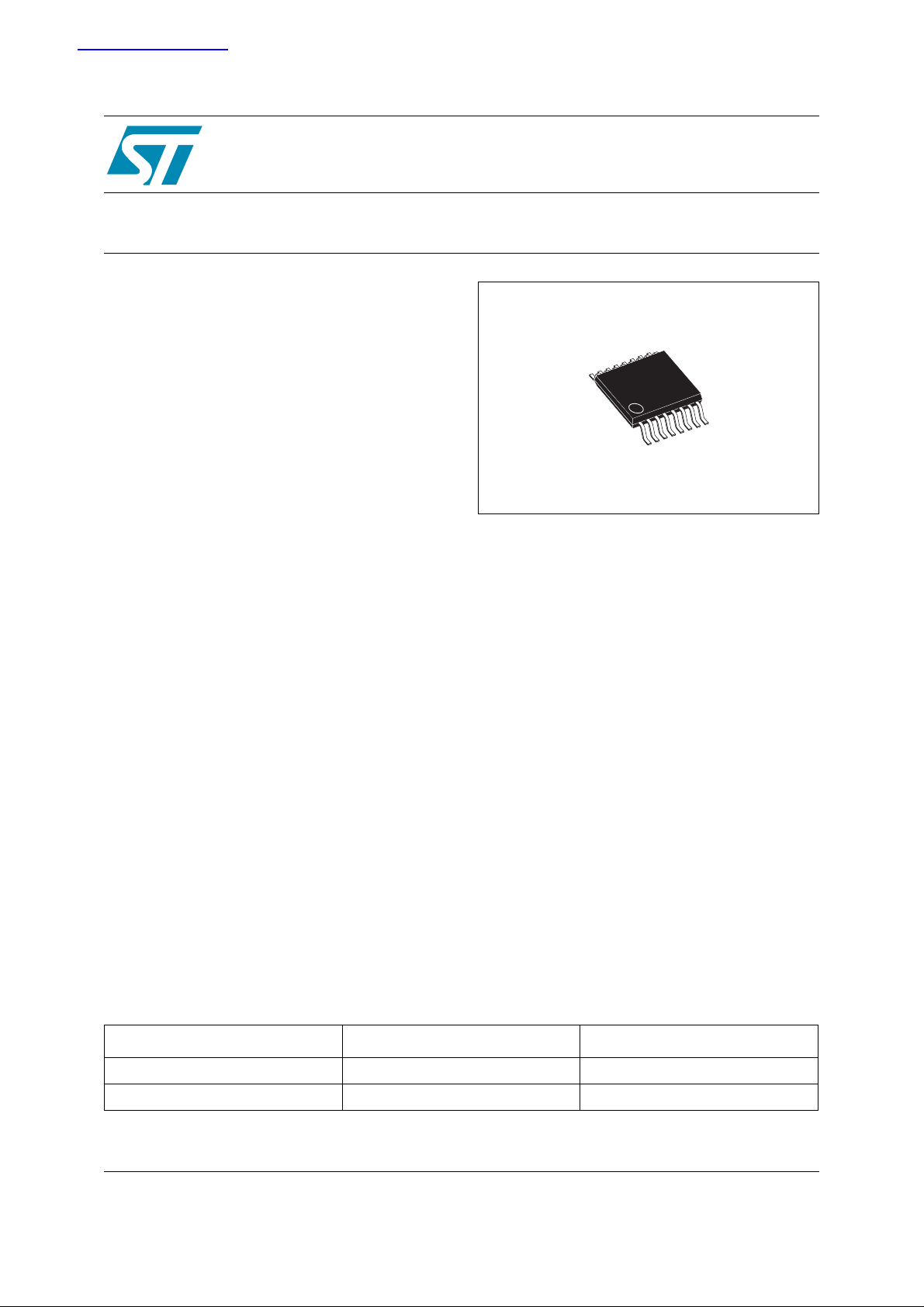
■ PACKAGE: HTSSOP16
LOWER THAN 100ns
ON
CONTROL
SIDE R
SENSE OVER-CURRENT-
DSON
PROTECTION
250KHz/500KHz
180° PHASE SHIFT
L6732C
HTSSOP16 (Exposed Pad)
Applications
■ HIGH PERFORMANCE / HIGH DENSITY DC-
DC MODULES
■ LOW VOLTAGE DISTRIBUTED DC-DC
■ niPOL CONVERTERS
■ DDR MEMORY SUPPLY
■ GRAPHIC CARDS
Order Codes
Part number Package Packing
L6732C HTSSOP16 Tube
L6732CTR HTSSOP16 Tape & Reel
Rev 1
December 2005 1/32
www.st.com
32
Page 2

L6732C
Contents
1 Summary Description . . . . . . . . . . . . . . . . . . . . . . . . . . . . . . . . . . . . . . . . . . 4
1.1 Functional Description . . . . . . . . . . . . . . . . . . . . . . . . . . . . . . . . . . . . . . . . . . 5
2 Electrical Data . . . . . . . . . . . . . . . . . . . . . . . . . . . . . . . . . . . . . . . . . . . . . . . . 6
2.1 Maximum Rating . . . . . . . . . . . . . . . . . . . . . . . . . . . . . . . . . . . . . . . . . . . . . . . 6
2.2 Thermal Data . . . . . . . . . . . . . . . . . . . . . . . . . . . . . . . . . . . . . . . . . . . . . . . . . 6
3 Pin Connections and Functions . . . . . . . . . . . . . . . . . . . . . . . . . . . . . . . . . . 7
4 Electrical Characteristics . . . . . . . . . . . . . . . . . . . . . . . . . . . . . . . . . . . . . . . 9
5 Device Description . . . . . . . . . . . . . . . . . . . . . . . . . . . . . . . . . . . . . . . . . . . 11
5.1 Oscillator . . . . . . . . . . . . . . . . . . . . . . . . . . . . . . . . . . . . . . . . . . . . . . . . . . . . .11
5.2 Internal LDO . . . . . . . . . . . . . . . . . . . . . . . . . . . . . . . . . . . . . . . . . . . . . . . . . .11
5.3 Bypassing the LDO to avoid the voltage drop with low Vcc . . . . . . . . . . . . . 12
5.4 Internal and External references . . . . . . . . . . . . . . . . . . . . . . . . . . . . . . . . . . 12
5.5 Error Amplifier . . . . . . . . . . . . . . . . . . . . . . . . . . . . . . . . . . . . . . . . . . . . . . . . 13
5.6 Soft Start . . . . . . . . . . . . . . . . . . . . . . . . . . . . . . . . . . . . . . . . . . . . . . . . . . . . 13
5.7 Driver Section . . . . . . . . . . . . . . . . . . . . . . . . . . . . . . . . . . . . . . . . . . . . . . . . 14
5.8 Monitoring and Protections . . . . . . . . . . . . . . . . . . . . . . . . . . . . . . . . . . . . . . 15
5.9 HICCUP Mode during an OCP . . . . . . . . . . . . . . . . . . . . . . . . . . . . . . . . . . . 17
5.10 Thermal shutdown . . . . . . . . . . . . . . . . . . . . . . . . . . . . . . . . . . . . . . . . . . . . 17
5.11 Synchronization . . . . . . . . . . . . . . . . . . . . . . . . . . . . . . . . . . . . . . . . . . . . . . 18
5.12 Minimum on-time (TON, MIN) . . . . . . . . . . . . . . . . . . . . . . . . . . . . . . . . . . . . 19
5.13 Bootstrap anti-discharging system . . . . . . . . . . . . . . . . . . . . . . . . . . . . . . . . 20
5.13.1 Fan's Power Supply . . . . . . . . . . . . . . . . . . . . . . . . . . . . . . . . . . . . . . . . . . . . 20
2/32
Page 3

L6732C
6 Application Details . . . . . . . . . . . . . . . . . . . . . . . . . . . . . . . . . . . . . . . . . . . 21
6.1 Inductor Design . . . . . . . . . . . . . . . . . . . . . . . . . . . . . . . . . . . . . . . . . . . . . . . 21
6.2 Output Capacitors . . . . . . . . . . . . . . . . . . . . . . . . . . . . . . . . . . . . . . . . . . . . . 22
6.3 Inp ut c apac it ors . . . . . . . . . . . . . . . . . . . . . . . . . . . . . . . . . . . . . . . . . . . . . . . 22
6.4 Compensation network . . . . . . . . . . . . . . . . . . . . . . . . . . . . . . . . . . . . . . . . . 23
7 L6732C Demoboard . . . . . . . . . . . . . . . . . . . . . . . . . . . . . . . . . . . . . . . . . . . 25
7.1 Description . . . . . . . . . . . . . . . . . . . . . . . . . . . . . . . . . . . . . . . . . . . . . . . . . . 25
8 Package Mechanical Data . . . . . . . . . . . . . . . . . . . . . . . . . . . . . . . . . . . . . . 29
9 Revision history . . . . . . . . . . . . . . . . . . . . . . . . . . . . . . . . . . . . . . . . . . . . . . 31
3/32
Page 4

1 Summary Description L6732C
1 Summary Description
The controller is an integrated circuit realized in BCD5 (BiCMOS-DMOS, version 5) fabrication
that provides complete control logic and protection for high performance step-down DC-DC and
niPOL converters.
It is designed to drive N-Channel MOSFETs in a synchronous rectified buck topology . The
output voltage of the converter can be precisely regulated down to 600mV with a maximum
tolerance of ±0.8% and it is also possible to use an external reference from 0V to 2.5V.
The input voltage can range from 1.8V to 14V, while the supply voltage can range from 4.5V to
14V. High peak current gate drivers provide for fast switching to the external power section, and
the output current can be in excess of 20A. The PWM duty cycle can range from 0% to 100%
with a minimum on-time (T
low duty cycle at high switching frequency. The device provides voltage-mode control that
includes a selectable frequency oscillator (250KHz or 500KHz).
The error amplifier features a 10MHz gain-bandwidth-product and 5V/µs slew-rate that permits
to realize high converter bandwidth for fast transient response. The device monitors the current
by using the R
current sensing resistor and guaranteeing an effective over-current-protection in all the
application conditions. When necessary, two different current limit protections can be externally
set through two external resistors.
DS(ON)
ON, MIN
of both the high-side and low-side MOSFET(s), eliminating the need for a
) lower than 100ns making possible conversions with very
During the soft-start phase a constant current protection is provided while after the soft-start the
device enters in hiccup mode in case of over-current. During the soft-start, the sink mode
capability is disabled in order to allow a proper start-up also in pre-biased output voltage
conditions. After the soft-start the device can sink current. Other features are Power-Good,
Master/Slave synchronization (with 180° phase shift), over-voltage-protection, feed-back
disconnection and thermal shutdown. The HTSSOP16 package allows the realization of really
compact DC/DC converters.
4/32
Page 5

L6732C 1 Summary Description
Vin=1.8V
-14V
L6732
C
FB SS
-
+
-
-
SS
-
- +
-
-
1.1 Functional Description
Figure 1. Block Diagram
OCH
Monitor
Monitor
OCH
OSC
OSC
+
+
0.6V
LDO
LDO
VCCDR
VCCDR
BOOT
BOOT
HGATE
HGATE
PHASE
PHASE
V
OUT
LGATE
LGATE
-
-
PGND
PGND
GND
GND
+
+
+
PWM
PWM
E/A
E/A
EAREF
EAREF
PGOOD
SYNCH
OCL
OCL
Protection and Ref
Protection and Ref
FB
COMP
COMP
5/32
Page 6
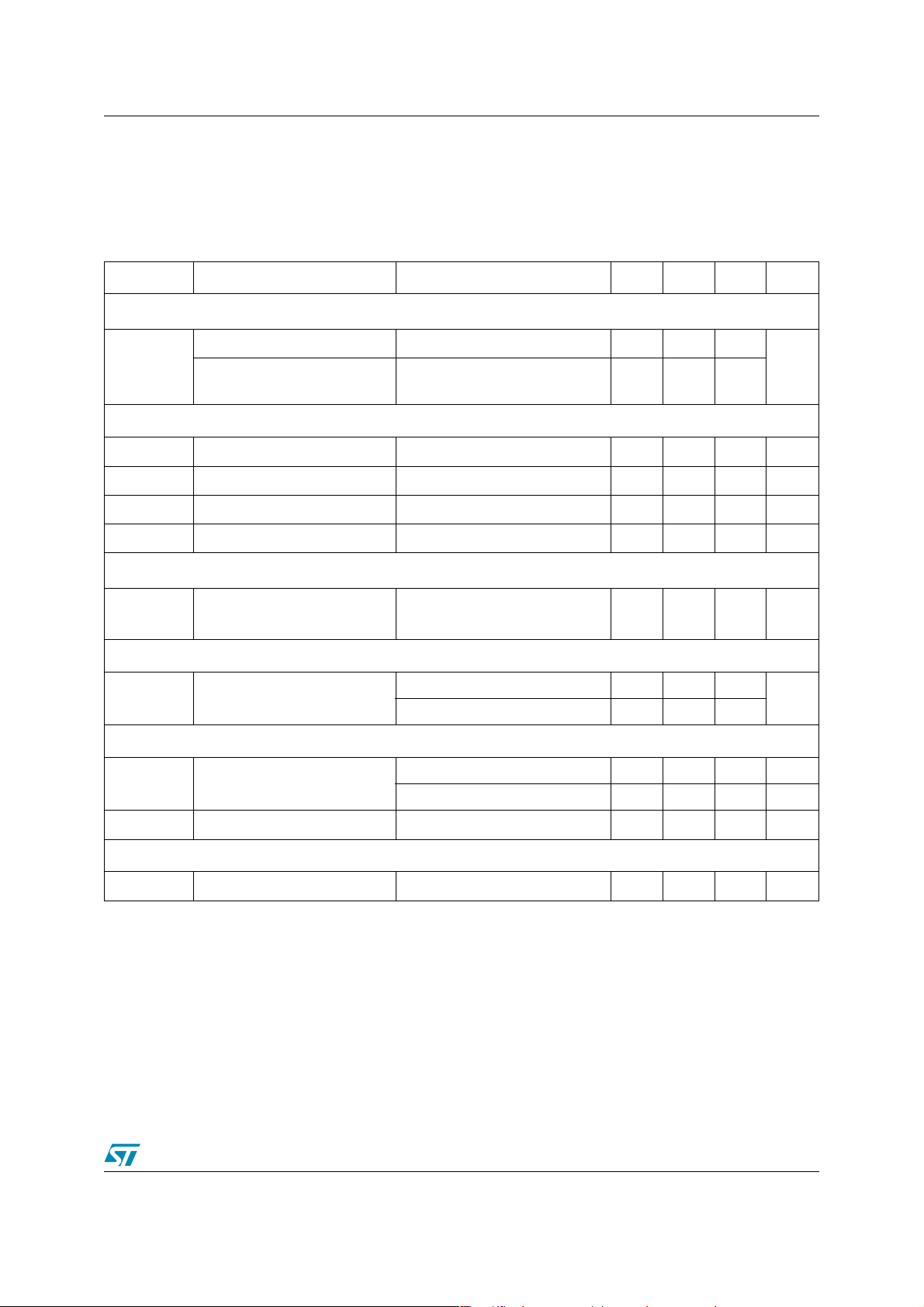
2 Electrical Data L6732C
2 Electrical Data
2.1 Maximum Rating
Tab le 1. Absolute maximum ratings
Symbol Parameter Value Unit
V
VCC to GND and PGND, OCH, PGOOD
CC
V
BOOT - VPHASE
V
HGATE - VPHASE
V
BOOT
V
PHASE
Boot V oltage 0 to 6 V
BOOT -0.3 to 24 V
PHASE -1 to 18
PHASE Sp ike, transient < 50ns (F
= 500KHz)
SW
-0.3 to 18 V
0 to V
BOOT
- V
PHASE
-3
+24
V
V
OCH Pin
SS, FB, EAREF, SYNC, OCL, LGATE, COM P, V
Maximum Withstanding Voltage Range
CCDR
-0.3 to 6 V
±1500
Test Condition: CDF-AEC-Q100- 002 "Human Body Model"
OTHER PINS ±2000
Acceptance Cri teria: "Normal Performance"
2.2 Thermal Data
Table 2. Thermal data
Symbol Description Value Unit
(1)
R
thJA
T
STG
T
J
T
A
1. Package mounted on demoboard.
Max. Thermal Resistance Junction to ambient 50 °C/W
Storage temperature range -40 to 150 °C
Junction operating temperature range -40 to 125 °C
Operative tempera tur e range -25 ~ +125 °C
VPGOOD Pin ±1000
6/32
Page 7
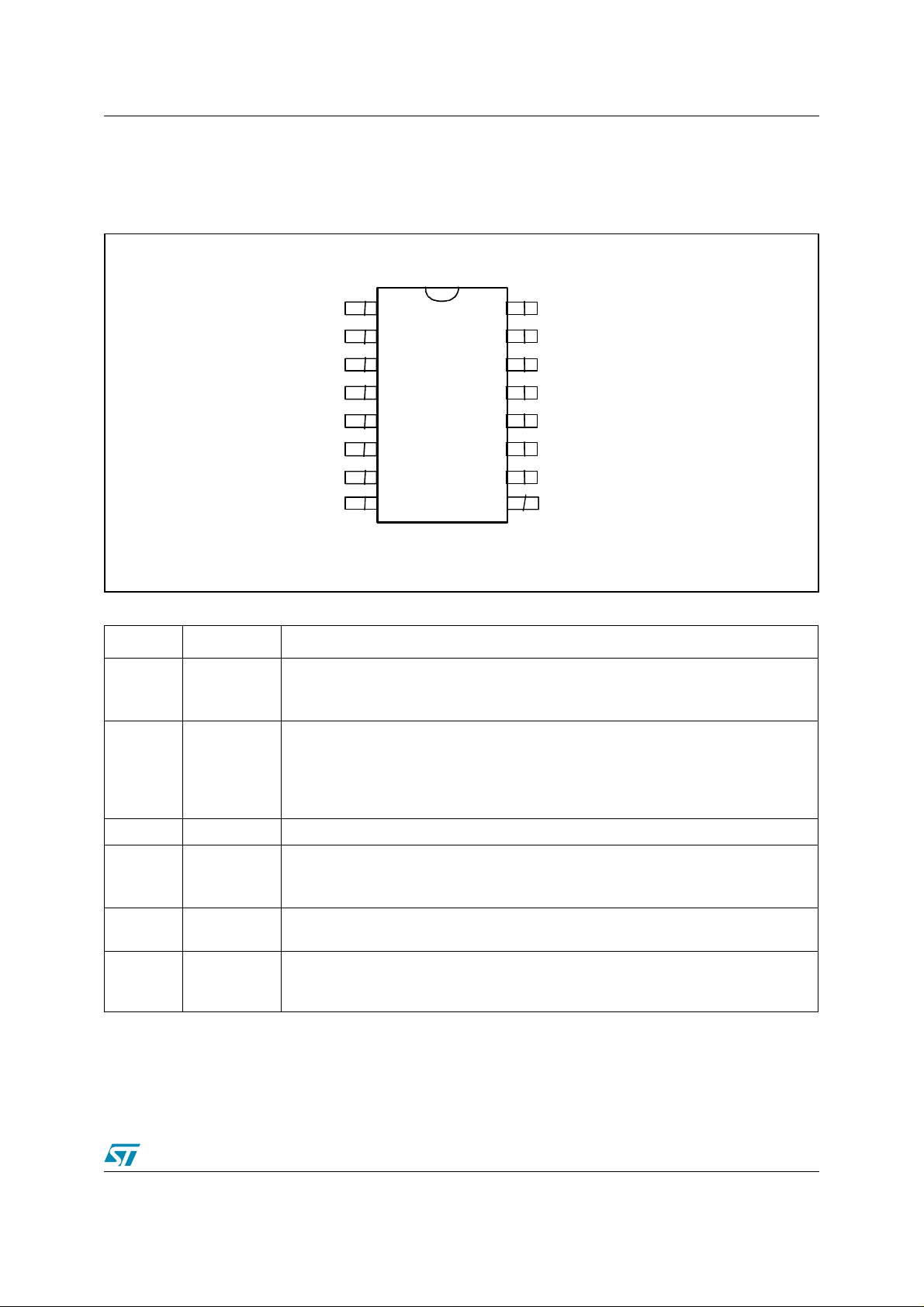
L6732C 3 Pin Connections and Functions
2 3 4
6
12
14 15 16
10
8
OCL
3 Pin Connectio ns and Functions
Figure 2. Pins Connection ( Top view)
PGOOD
SYNCH
1
SGND
FB
COMP
SS/INH
EAREF
Table 3. Pin Functions
Pin n. Name Function
This pin is an open collector output and it is pull ed low if the output voltage is not
1 PGOOD
2 SYNCH
within the specified thresholds (90%-1 10% ). If not used it may be lef t floating. Pull-up
this pin to V
It is a Master-Slave pin. Two or more devices can be synchronized by simply
connecting the SYNCH pins together. The device operating with the highest F
be the Master. The Slave devic es wil l operate with 180° pha se shift from the Master.
The best way to synchronize devic es toget her is to set thei r FSW at the same valu e. If
it is not used the SYNCH pin can be left floati ng.
5
7
HTSSOP16
with a 10K resistor to obtain a logical signal.
CCDR
13
11
9
VCC
VCCDR
LGATE
PGND
BOOT
HGATE
PHASE
OCH
SW
will
3 SGND All the inter nal references are referred to this pin.
This pin is connected to the error amplifier inverting input. Connect it to V
4 FB
5 COMP
6 SS/INH
the compensation net work. This pin is also used to sense the output volt age in order
to manage the over voltage conditions and the PGood signal.
This pin is connected to t he error amplifier output and is used to compensate the
voltage control feedback loop.
The soft-st art time is program m ed connecting an external capacitor fr om this pin and
GND. The internal current generator forces a current of 10 A through t he capacitor.
When the vol tage at this pin is lower than 0.5V the device is disabled.
OUT
through
7/32
Page 8
3 Pin Connections and Functions L6732C
S
---
---
Table 3. Pin Functions
By setting the voltage at this pin is possible to select the internal /external re ference
and the switching frequency:
7 EAREF
8 OCL
9 OCH
0-80% of V
V
EAREF
V
V
= 80%-95% of V
EAREF
= 95%-100% of V
EAREF
An internal clamp limits the maximum V
analog value presen t at this pin at the start-up when V
A resistor connec ted f rom this pin to ground se ts the valley- current-limit. The valley
current is sensed through the low-side MOSFET(s). The internal current generator
sources a current of 100µA (I
(R
). The over- current threshold i s given by the following equation:
OCL
Connecting a capacitor from this pin to GND helps in reducing the noise injected from
to the device, but can be a low impedanc e path for the high-frequency noise
V
CC
related to the GND. Connect a cap acitor only to a "clean" GND.
A resistor connected from this pin and the high-side MOSFET(s) dr ain sets the peak-
current-limit . The peak current is sensed through the high-si de MOSFET(s). The
internal 100µA current generator (I
external resistor (R
equation:
-> External Reference/FSW=250KHz
CCDR
-> V
CCDR
CCDR -> VREF
OCL
). The over-current threshold i s giv en by the following
OCH
= 0.6V/FSW=500KHz
REF
= 0.6V/FSW=250KHz
at 2.5V (typ.). The devi ce captures the
EAREF
meets the UVLO threshol d.
CC
) from this pin to ground through the external resistor
I
•
I
VALLEY
OCH
I
PEAK
OCLIOCL
=
----------------------------2R
•
DSONL
) sinks a current fro m the drai n through the
I
•
OCHROCH
------------------------------
=
R
DSONHS
This pin is connected to t he source of the high-side MOSFET(s) and provides the
10 PHASE
return path for the high-side dr iver. This pin monitors the drop across both the upper
and lower MOSFET(s) for the current li m it together with OCH and OCL.
1 1 HGATE This pin is connected to the high-side MOSFET(s) gat e.
12 BOOT
13 PGND
Through this pin is supplied the high-side driver. Connect a capacitor from this pin to
the PHASE pin and a diode from V
to this pin (cathode versus BOOT).
CCDR
This pin has to be connected closely to the low-side MOSFET(s) source in order to
reduce the noise injection into the device.
14 LGATE This pin is connected to t he low-side MOSFET(s) gate.
15
16
V
CCDR
V
CC
5V internally regulated voltage. It is used to supply the inter nal drivers. Fil ter it to
ground with at least 1µF ceramic cap.
Supply voltag e pin. The operative supply voltage range is from 4.5V to 14V.
8/32
Page 9
L6732C 4 Electrical Char acteristics
4 Electrical Characteristics
V
= 12V, TA = 25°C unless otherwise specified.
CC
Table 4. Electrical Characteristics
Symbol Parameter Test Condition Min. Typ. Max. Unit
V
Supply Current
CC
VCC Stand By current
I
CC
quiescent current
V
CC
Power-ON
V
CC
Turn-ON VCC thresh o ld V
Turn-OFF V
V
CCDR
V
V
IN OK
IN OK
Regulation
Turn-ON V
Turn-OFF V
V
CCDR
Soft Start and Inhibit
I
SS
Soft Start Current
Oscillator
f
OSC
Accuracy
CC
OCH
OCH
voltage
threshold V
thresh ol d
threshold
OSC = open; SS to GND 4.5 6.5
OSC= open;
HG = open, LG = open, PH=open
= 1.7V
OCH
= 1.7V
OCH
4.0 4.2 4.4 V
3.6 3.8 4.0 V
8.5 10
1.1 1.25 1.47 V
0.9 1.05 1.27 V
=5.5V to 14V
V
CC
= 1mA to 100mA
I
DR
4.5 5 5.5 V
SS = 2V 7 10 13
SS = 0 to 0.5V 20 30 45
237 250 263 KHz
450 500 550 KHz
mA
µA
∆V
OSC
Output Voltage
V
FB
Ramp Amplitude 2.1 V
= 0 to Vth
Output Voltage
V
DIS
0.597 0.6 0.603 V
9/32
Page 10

L6732C
Table 4. Electri cal C harac teris tics
Symbol Parameter Test Condition Min. Typ. Max. Unit
Error Amplifier
R
EAREF
I
FB
Ext Ref
Clamp
V
OFFSET
G
V
EAREF Input Resistance Vs. GND 70 100 150 kΩ
I.I. bias current
V
FΒ
0.290 0.5 µA
= 0V
2.3 V
Error amplifier offset Vref = 0.6V -5 +5 mV
Open Loop Voltage Gain Guaranteed by design 100 dB
GBWP Gain-Bandwidth Product Guaranteed by design 10 MHz
SR Slew-Rate
COMP = 10pF
Gua r anteed by desig n
5V/µs
Gate Drivers
R
HGATE_ON
R
HGATE_OFF
R
LGATE_ON
R
LGATE_OFF
High Side Sour ce Resistance
High Side Sink Resistance
Low Side Source Resistance
Low Side Sink Resistance
BOOT
V
BOOT
V
CCDR
V
CCDR
- V
- V
= 5V
= 5V
PHASE
PHASE
= 5V
= 5V
1.7 Ω
1.12 Ω
1.15 Ω
0.6 Ω
V
Protections
I
OCH
I
OCL
OVP
OCH Current Source
OCL Current Source 90 100 110 µΑ
Over Voltage Trip
(VFB / VEAREF)
V
OCH
V
FB
V
EAREF
V
FB
V
EAREF
= 1.7V
Rising
= 0.6V
Falling
= 0.6V
90 100 110 µΑ
120 %
117 %
Power Good
V
PGOOD
Upper Threshold
(V
FB
/ V
EAREF
)
Lower Threshold
(V
FB
/ V
EAREF
)
PGOOD Voltage Low IPGOOD = -5mA 0.5 V
V
FB
V
FB
Rising
Falling
108 110 112 %
88 90 92 %
Table 5. Therm al Character istics (VCC = 12V)
Symbol Parameter Test Condition Min. Typ. Max. Unit
Output Voltage
= 0°C~ 125°C
T
V
FB
Output Voltage
J
T
= -40°C~ 125°C
J
0.596 0.6 0.605
V
0.593 0.6 0.605
10/32
Page 11

L6732C 5 Device Descr iption
5 Device Description
5.1 Oscillator
The switching frequency can be fixed to two values: 250KHz or 500KHz by setting the proper
voltage at the EAREF pin (see Table 3. Pins function and section 4.3 Internal and external
reference).
5.2 Internal LDO
An internal LDO supplies the internal circuitry of the device. The input of this stage is the VCC
pin and the output (5V) is the V
Figure 3. LDO block diagram.
pin (Figure 3.).
CCDR
4.5V÷14V
The LDO can be by-passed, providing directly a 5V voltage to V
V
CCDR
least 1µF capacitor to sustain the internal LDO during the recharge of the bootstrap capacitor.
V
CCDR
LDO
. In this case VCC and
pins must be shorted together as shown in Figure 4. V
also represents a voltage reference for PGOOD pin (see Table 3. Pins Function).
CCDR
pin must be filtered with at
CCDR
11/32
Page 12

5 Device Descr iption L6732C
5.3 Bypassing the LDO to avoid the voltage drop with low Vcc
If V
≈5V the internal LDO works in dropout with an output resistance of about 1Ω. The
CC
maximum LDO output current is about 100mA and so the output voltage drop is 100mV, to
avoid this the LDO can be bypassed.
Figure 4. Bypassing the LDO
5.4 Inter nal and External references
It is possible to set the internal/external reference and the switching frequency by setting the
proper voltage at the EAREF pin. The maximum value of the external reference depends on the
V
: with V
CC
maximum external reference is 2.5V (typ.).
● V
EAREF
● V
EAREF
● V
EAREF
Providing an external reference from 0V to 450mV the output voltage will be regulated but
some restrictions must be considered:
● The minimum OVP threshold is set at 300mV;
● The under-voltage-protection doesn't work;
● The PGOOD signal remains low;
To set the resistor divider it must be considered that a 100K pull-down resistor is integrated into
the device (see Figure 5.). Finally it must be taken into account that the voltage at the EAREF
pin is captured by the device at the start-up when V
= 4V the clamp operates at about 2V (typ.), while with VCC greater than 5V the
CC
from 0% to 80% of V
from 80% to 95% of V
from 95% to 100% of V
-> External reference/Fsw = 250KHz
CCDR
-> V
CCDR
CCDR
-> V
REF
REF
= 0.6V/Fsw = 500KHz
= 0.6V/Fsw = 250KHz
is about 4V.
CC
12/32
Page 13

L6732C 5 Device Descr iption
5.5 Error Amplifier
Figure 5. Error Amplifi er Referenc e
5.6 Soft Start
When both VCC and VIN are above their turn-ON thresholds (VIN is monitored by the OCH pin)
the start-up phase takes place. Otherwise the S S pin is internally shorted to GND. At start-up, a
ramp is generated charging the external capacitor C
initial value for this current is 35µA and charges the capacitor up to 0.5V. After that it becomes
10µA until the final charge value of approximately 4V (see Figure 6.). The reference of the error
amplifier is clamped with this voltage (V
can always sink cu rrent
Figure 6. Device start-up: Voltage at the SS pin.
SS
with an internal current generator. The
SS
) until it reaches the programmed value. The Device
V
CC
V
IN
13/32
Page 14

5 Device Descr iption L6732C
If an over current is detected during the soft-start phase, the device provides a constantcurrent-protection. In this way, in case of short soft-start time and/or small inductor value and/or
high output capacitors value and so, in case of high ripple current during the soft-start, the
converter can start in any case, limiting the current (see section 4.6 Monitoring and protections)
but not entering in HICCUP mode. During normal operation, if any under-voltage is detected on
one of the two supplies, the SS pin is internally shorted to GND and so the SS capacitor is
rapidly discharged.
5.7 Driver Section
The high-side and low-side drivers allow using different types of power MOSFETs (also multiple
MOSFETs to reduce the R
supplied by V
while the high-side driver is supplied by the BOOT pin. A predictive dead
CCDR
time control avoids MOSFETs cross-conduction maintaining very short dead time duration in
the range of 20ns. The control monitors the phase node in order to sense the low-side body
diode recirculation. If the phase node voltage is less than a certain threshold (-350mV typ.)
during the dead time, it will be reduced in the next PWM cycle. The predictive dead time control
doesn't work when the high-side body diode is conducting because the phase node doesn't go
negative. This situation happens when the converter is sinking current for example and, in this
case, an adaptive dead time control operates.
), maintaining fast switching transitions. The low-side driver is
DSON
14/32
Page 15

L6732C 5 Device Descr iption
5.8 Monitoring and Protections
The output voltage is monitored by means of pin FB. If it is not within ±10% (typ.) of the
programmed value, the Power-Good (PGOOD) output is forced low.
The device provides over-voltage-protection: when the voltage sensed on FB pin reaches a
value 20% (typ.) greater than the reference, the low-side driver is turned on as long as the over
voltage is detected (see Figure 7.).
Figure 7. OVP
LGate
FB
It must be taken into account that there is an electrical network between the output terminal and
the FB pin and therefore the voltage at the pin is not a perfect replica of the output voltage.
However due to the fact that the converter can sink current, in the most of cases the low-side
will turn-on before t he ou tpu t voltage exceeds the over-voltag e threshold, because the error
amplifier will throw off balance in advance. Even if the device doesn't report an over-voltage,
the behavior is the same, because the low-side is turned-on immediately. The following figure
shows the device behavior during an over-voltage event. The output voltage rises with a slope
of 100mV/µs, emulating in this way the breaking of the high-side MOSFET as an over-voltage
cause.
15/32
Page 16

5 Device Descr iption L6732C
L
Figure 8. OVP: the low-side MOSFET is turned-on in advance.
V
OUT
109%
V
FB
LGate
The device realizes the over-current-protection (OCP) sensing the current both on the highside MOSFET(s) and the low-side MOSFET(s) and so 2 current limit thresholds can be set (see
OCH pin and OCL pin in Table 3. Pins function):
● Peak Current Limit
● Valley Curre nt L imit
The Peak Current Protection is active when the high-side MOSFET(s) is turned on, after a
masking time of about 100ns. The valley-current-protection is enabled when the low-side
MOSFET(s) is turned on after a masking time of about 400ns. If, when the soft-start phase is
completed, an over current event occurs during the on time (peak-current-protection) or during
the off time (valley-current-protection) the device enters in HICCUP mode: the high-side and
low-side MOSFET(s) are turned off, the soft-start capacitor is discharged with a constant
current of 10µA and when the voltage at the SS pin reaches 0.5V the soft-start phase restarts.
During the soft-start phase the OCP provides a constant-current-protection. If during the T
ON
the OCH comparator triggers an over current the high-side MOSFET(s) is immediately turned
off (after the masking time and the internal delay) and returned on at the next pwm cycle. The
limit of this protection is that the T
can't be less than masking time plus propagation delay
ON
because during the masking time the peak-current-protection is disabled. In case of very hard
short circuit, even with this short T
, the current could escalate. The valley-current-protection
ON
is very helpful in this case to limit the current.
If during the off-time the OCL comparator triggers an over current, the high-side MOSFET(s) is
not turned on until the current is over the valley-current-limit. This implies that, if it is necessary,
some pulses of the high-side MOSFET(s) will be skipped, guaranteeing a maximum current
due to the following formula:
VoutVin
II
−
+=
T
⋅
(4)
MINONVALLEYMAX
,
In constant current protection a current control loop limits the value of the error amplifier output
(comp), in order to avoid its saturation and thus recover faster when the output returns in
regulation. Figure 9. shows the behaviour of the device during an over current condition that
persists also in the soft-start phase.
16/32
Page 17

L6732C 5 Device Descr iption
5.9 HICCUP Mode during an OCP
Figure 9. Constant current and Hiccup Mode during an OCP.
VSS
VCOMP
I
L
5.10 Thermal shutdown
When the junction temperature reaches 150°C ±10°C the device enters in thermal shutdown.
Both MOSFETs are turne d off and the soft-start capacitor is rapidly discharged with an internal
switch. The device doesn't restart until the junction temperature goes down to 120°C and, in
any case, until the voltage at the soft-start pin reaches 500mV.
17/32
Page 18

5 Device Descr iption L6732C
5.11 Synchronization
The presence of many converters on the same board can generate beating frequency noise. T o
avoid this it is important to make them operate at the same switching frequency. Moreover, a
phase shift between different modules helps to minimize t he RMS curr ent on t he common input
capacitors. Fi gu r e 10 . and Figure 11. shows the results of two modules in synchronization. Two
or more devices can be synchronized simply connecting together the SYNCH pins. The device
with the higher switching frequency will be the Master while the other one will be the Slave. The
Slave controller will increase its switching frequency reducing the ramp amplitude
proportionally and then the modulator gain will be increased.
Figure 10. Synchronizatio n: PWM Signal
Figure 11. Synchr onization: I nductor Currents
To avoid a huge variation of the modulator gain, the best way to synchronize two or more
devices is to make them work at the same switching frequency and, in any case, the switching
frequencies can differ for a maximum of 50% of the lowest one. If, during synchronization
between two (or more) L6732C, it's important to know in advance which the master is, it's timely
to set its switching frequency at least 15% higher than the slave. Using an external clock signal
(f
) to synchronize one or more devices that are working at a different switching frequency
EXT
(f
) it is recommended to follow the below formula:
SW
fff ⋅≤≤ 3,1
SWEXTSW
The phase shift between master and slaves is approximately 180°.
18/32
Page 19

L6732C 5 Device Descr iption
5.12 Minimum on-time (TON,
The device can manage minimum on-times lower than 100ns. This feature comes down from
the control topology and from the particular over-current-protection system of the L6732C. In
fact, in a voltage mode controller the current has not to be sensed to perform the regulation
and, in the case of L6732C, neither for the over-current protection, given that during the off-time
the valley-current-protection can operate in every case. The first advantage related to this
feature is the possibility to realize extremely low conversion ratios. Figure 12. shows a
conversion from 14V to 0.3V at 500KHz with a T
Figure 12. 14V -> 0.3V@500KHz, 5A
MIN
)
of about 50ns.
ON
V
OUT
I
L
VPHASE
50ns
The on-time is limited by the turn-on and turn-off times of the MOSFETs.
19/32
Page 20

5 Device Descr iption L6732C
5.13 Bootstrap anti-discharging system
This built-in system avoids that the voltage across the bootstrap capacitor becomes less than
3.3V. An internal comparator senses the voltage across the external bootstrap capacitor
keeping it charged, eventually turning-on the low-side MOSFET for approximately 200ns. If the
bootstrap capacitor is not enough charged the high-side MOSFET cannot be effectively turnedon and it will present a higher R
bootstrap capacitor can be discharged during the soft-start in case of very long soft-start time
and light loads. It's also possible to mention one application condition during which the
bootstrap capacitor can be discharged:
5.13.1 Fan's Power Supply
In many applications the FAN is a DC MO TOR driven by a voltage-mode DC/DC converter.
Often only the speed of the MOTOR is controlled by varying the voltage applied to the input
terminal and there's no control on the torque because the current is not directly controlled. In
order to vary the MOTOR speed the output voltage of the converter must be varied. The
L6732C has a dedicated pin called EAREF (see the related section) that allows providing an
external reference to the non-inverting input of the error-amplifier.
In these applications the duty cycle depends on the MOTOR's speed and sometimes 100% has
to be set in order to go at the maximum speed. Unfortunately in these conditions the bootstrap
capacitor can not be recharged and the system cannot work properly. Some PWM controller
limits the maximum duty-cycle to 80-90% in order to keep the bootstrap cap charged but this
make worse the performance during the load transient. Thanks to the "bootstrap antidischarging system" the L6732C can work at 100% without any problem. The following picture
shows the device behaviour when input voltage is 5V and 100% is set by the external
reference.
. In some cases the OCP can be also triggered. The
DSON
Figure 13. 100% DUTY CYCLE OPERATION
20/32
Page 21

L6732C 6 Application Details
t
INDUCTOR CURRENT RIPPL E
Vin =5V, L=500nH
6 Application Details
6.1 Inductor Design
The inductance value is defined by a compromise between the transient response time, the
efficiency , the cost and the size. The inductor has to be calculated to sustain the output and the
input voltage variation to maintain the ripple current (∆I
maximum output current. The inductance value can be calculated with the following
relationship:
−
≅
L
VoutVin
Vou
⋅
∆⋅
Vin
IFsw
L
) between 20% and 30% of the
L
(6)
Where F
Figure 14. shows the ripple current vs. the output voltage for diff erent values of the inductor,
with V
Figure 14. Inductor current ripple.
8
7
6
5
4
3
2
1
0
01234
Increasing the value of the inductance reduces the ripple current but, at the same time,
increases the converter response time to a load transient. If the compensation network is well
designed, during a load transient the device is able to set the duty cycle to 100% or to 0%.
When one of these conditions is reached, the response time is limited by the time required to
change the inductor current. During this time the output current is supplied by the output
capacitors. Minimizing the response time can minimize the output capacitor size.
is the switching frequency, VIN is the input voltage and V
SW
= 5V and VIN = 12V at a switching frequency of 500KHz.
IN
OUTPUT VOLTAGE (V)
is the output voltage.
OUT
Vin =12V, L =1uH
Vin =12V, L =2uH
Vin =5V, L=1.5uH
21/32
Page 22

6 Application Details L6732C
R
)
)
t
)
Vout
Cout
2
)
8
Fsw
Cout
)
)
)
2
)
)
6.2 Output Capacitors
The output capacitors are basic components for the fast transient response of the power
supply. They depend on the output voltage ripple requirements, as well as any output voltage
deviation requirement during a load transient. During a load transient, the output capacitors
supply the current to the load or absorb the current stored in the inductor until the converter
reacts. In fact, even if the controller recognizes immediately the load transient and sets the duty
cycle at 100% or 0%, the current slope is limited by the inductor value. The output voltage has
a first drop due to the current variation inside the capacitor (neglecting the effect of the ESL):
ES
IoutVout
ESR
Moreover, there is an additional drop due to the effective capacitor discharge or charge that is
given by the following formulas:
Vout
Formula (8) is valid in case of positive load transient while the formula (9) is valid in case of
negative load transient. D
a given inductor value, minimum input voltage, output voltage and maximum load transient , a
maximum ESR and a minimum C
the static output voltage ripple. In the worst case the output voltage ripple can be calculated
with the following formula:
Usually the voltage drop due to the ESR is the biggest one while the drop due to the capacitor
discharge is almost negligible.
COUT
=∆
Vout
is the maximum duty cycle value that in the L6732C is 100%. For
MAX
=∆
COUT
value can be set. The ESR and C
OUT
(
ESRIVout
L
⋅∆=∆
2
2
⋅⋅
+⋅∆=∆
(7
LIout
⋅∆
maxmin,(2
DVinCout
LIout
⋅∆
−⋅⋅⋅
(9)
Vou
1
(10
(8
values also affect
OUT
⋅⋅
6.3 Input capacitors
The input capacitors have to sustain the RMS current flowing through them, that is:
Where D is the duty cycle. The equation reaches it s maximu m value, I
losses in worst case are:
22/32
(12
(11
/2 with D = 0.5. The
OUT
1( DDIoutIrms −⋅⋅=
5.0( IoutESRP ⋅⋅=
Page 23

L6732C 6 Application Details
000000000000000000000000000000
t
Cout
ESR
6.4 Compensation network
The loop is based on a voltage mode control (Figure 15.). The output voltage is regulated to the
internal/external reference voltage and scaled by the external resistor divider. The error
amplifier ou tput V
width modulated (PWM) with an amplitude of V
by the output filter. The modulator transfer function is the small signal transfer function of V
V
. This function has a double pole at frequency FLC depending on the L-C
COMP
and a zero at FESR depending on the output capacitor's ESR. The DC Gain of the modulator is
simply the input voltage V
Figure 15. Compensation Network
is then compared with the oscillator triangular wave to provide a pulse-
COMP
divided by the peak-to-peak oscillator voltage: V
IN
at the PHASE node. This waveform is filtered
IN
OUT
.
OSC
resonance
OUT
/
Z
FB
The compensation network consists in the internal error amplifier, the impedance networks Z
(R3, R4 and C20) and Z
closed loop transfer function with the highest 0dB crossing frequency to have fastest transient
response (but always lower than fsw/10) and the highest gain in DC conditions to minimize the
load regulation error. A stable control loop has a gain crossing the 0dB axis with -20dB/decade
slope and a phase margin greater than 45°. To locate poles and zeroes of the compensation
networks, the following suggestions may be used:
● Modula tor singularity frequencies:
ω
LC
● Compensation network singularity frequencies:
ω
=
P
1
R
(R5, C18 and C19). The compensation network has to provide a
FB
=
1
Cou
L
⋅
1
⎛
⋅
⎜
⋅
5
⎜
⎝
CC
+
(13)
(15)
⎞
1918
⎟
⎟
CC
1918
⎠
ω
ESR
ω
=
P
1
⋅
1
=
2
⋅
CR
Z
IN
IN
(14)
(16)
204
ω
1
Z
1
=
CR
⋅
(17) (18)
195
ω
=
2
Z
1
()
RRC
+⋅
4320
23/32
Page 24

6 Application Details L6732C
● Compensation network design:
– Put the gain R
ω
–Place
–Place
–Place
–Place
– Check the loop gain considering the error amplifier open loop gain.
Figure 16. Asymptot ic Bode plot of Conv e rt er's op e n l oop ga i n
before the output filter resonance ωLC;
Z1
ω
at the output filter resonance ωLC;
Z2
ω
at the output capacitor ESR zero ω
P1
ω
at one half of the switching frequency;
P2
in order to obtain the desired converter bandwidth
5/R3
Vin
R
5
⋅=
∆
R
3
Vosc
ϖϖ
⋅
(19)
LCC
;
ESR
24/32
Page 25

L6732C 7 L6732C Demoboard
9
U1
T
12
O
CH
T
R9 C9 13 14
HGATE PHASE LGATE PGND
VCC
1
6 VCC
SS
BOOT
15
VCCDR
5
VFB COMP
C1 R2 C2 C3 R4 R7
EAREF
4 3
GND
G
IN
OCL
R6 R5 C8
PGOOD SYNCH
2
SYNCH
PGOOD
R
13
7 L6732C Demoboard
7.1 Description
L6732C demoboard realizes in a four layer PCB a step-down DC/DC converter and shows the
operation of the device in a general purpose application. The input voltage can range from 4.5V
to 14V and the output voltage is at 3.3V . The module can deliver an output current in excess of
20A. The switching frequency is set at 250 KHz (controller free-running F
to 500KHz acting on the EAREF pin.
Figure 17. Demoboard schematic
VIN
C10
EXT REF
VCCDR
C5
R8
C7
D1
7
L6732
C
C11
11
10
R11
R10
Q4-6
Q1-3
R12
D3
C15
) but it can be set
SW
C12-C13
L1
C16-C19
VOU
GOU
1
8
Table 6. Demob oar d part list
Reference Value Manufacturer Package Supplier
R1 1k
R2 1k
R3 4K7
R4 2k7 Neohm SMD 0603 IFARCAD
R5 0
R6 N.C. Neohm SMD 0603 IFARCAD
R7 2K Neohm SMD 0603 IFARCAD
R8 10
R9 1K5 Neohm SMD 0603 IFARCAD
Ω Neohm SMD 0603 IFARCAD
Ω Neohm SMD 0603 IFARCAD
Ω Neohm SMD 0603 IFARCAD
Ω Neohm SMD 0603 IFARCAD
6
C4
R3
R1
25/32
Page 26

7 L6732C Demoboard L6732C
Table 6. Demob oar d part list
R10 2.2Ω Neohm SMD 0603 IFARCAD
R11 2.2
Ω Neohm SMD 0603 IFARCAD
R12 N.C. Neohm SMD 0603 IFARCAD
R13 10K
Ω Neohm SMD 0603 IFARCAD
C1 4.7nF Kemet SMD 0603 IFARCAD
C2 47nF Kemet SMD 0603 IFARCAD
C3 1nF Kemet SMD 0603 IFARCAD
C4 100nF Kemet SMD 0603 IFARCAD
C5 100nF Kemet SMD 0603 IFARCAD
C6 N.C. / / /
C7 100nF Kemet SMD 0603 IFARCAD
C8 4.7uF 20V AVX SMA6032 IFARCAD
C9 1nF Kemet SMD 0603 IFARCAD
C10 1uF Kemet SMD 0603 IFARCAD
C11 220nF Kemet SMD 0603 IFARCAD
C12-13 3X 15uF / / ST (TDK)
C15 N.C. / / /
C16-19 2X 330uF / / ST (poscap)
L1 1.8uH Panasonic SMD ST
D1 STPS1L30M ST DO216AA ST
D3 STPS1L30M ST DO216AA ST
Q1-Q2 STS12NH3LL ST SO8 ST
Q4-Q5 STS25NH3LL ST SO8 ST
U1 L6732C ST HTSSOP16 ST
Table 7. Other inductor manufacturer
Manufacturer Series Inductor Value (µH) Saturation Current (A)
WURTH ELEKTRONIC 744318180 1.8 20
SUMIDA CDEP134-2R7MC-H 2.7 15
EPCOS HPI_13 T640 1.4 22
TDK SPM12550T-1R0M220 1 22
TOKO FDA1254 2.2 14
COILTRONICS
HCF1305-1R0 1.15 22
HC5-1R0 1.3 27
26/32
Page 27

L6732C 7 L6732C Demoboard
EFFICIEN
Table 8. Othe r capacitor manufactur er
Manufacturer Series Capacitor value(µF) Rated voltage (V)
TDK
C4532X5R1E156M 15 25
C3225X5R0J107M 100 6.3
NIPPON CHEMI-CON 25PS100MJ12 100 25
PANASONIC ECJ4YB0J107M 100 6.3
Figure 18. Demoboard efficiency
Fsw =400KHz
FSW = 500 KHz
95.00%
90.00%
85.00%
80.00%
75.00%
= 5V
V
IN
= 12V
V
IN
1 3 5 7 9 11 13 15
Iout (A)
Figure 19. PCB Layout: Top Layer
Figure 20. P CB Layout: Power Ground Layer
27/32
Page 28

7 L6732C Demoboard L6732C
Figure 21. PCB Layout: Signal-Ground Layer
Figure 22. PCB Layout: Bottom Layer
28/32
Page 29

L6732C 8 Package Mechanical Data
8 Package Mechanical Da ta
In order to meet environmental requirements, ST offers these devices in ECOPACK®
packages. These packages have a Lead-free second level interconnect . The category of
second Level Interconnect is marked on the package and on the inner box label, in compliance
with JEDEC Standard JESD97. The maximum ratings related to soldering conditions are also
marked on the inner box label. ECOPACK is an ST trademark. ECOPACK specifications are
available at: www.st.com.
29/32
Page 30

8 Package Mechani cal Data L6732C
Table 9. HTSSOP 16 M echan ical Data
mm. inch
DIM.
MIN. TYP MAX. MIN. TYP. MAX.
A 1.2 0.047
A1 0.15 0.004 0.006
A2 0.8 1 1.05 0.031 0.039 0.041
b 0.19 0.30 0.007 0.012
c 0.09 0.20 0.004 0.0089
D 4.9 5 5.1 0.193 0.197 0.201
D1 1.7 0.067
E 6.2 6.4 6.6 0.244 0.252 0.260
E1 4.3 4.4 4.5 0.169 0.173 0.177
E2 1.5 0.059
e 0.65 0.0256
K0° 8°0° 8°
L 0.45 0.60 0.75 0.018 0.024 0.030
Figure 23. Package Dimensions
30/32
7419276A
Page 31

L6732C 9 Revision history
9 Revision history
Date Revision Changes
12-Dec-2005 1 In it ial release.
31/32
Page 32

9 Revision his tor y L6732C
I
s
o
d
b
ct
t
ot
a
nformation furnished is believed to be accurate and reliable. However, STMicroelectronics assumes no responsibility for the consequence
f use of such information nor for any infringement of patents or other rights of third parties which may result from its use. No license is grante
y implic ation or otherwise unde r any patent or patent rights of STMicroelectronics. Speci fications me nt i oned in this publication are subje
o change without notice. This publication supersedes and replaces all information previously supplied. STMicroelectronics products are n
uthoriz ed for use as critical component s in l i fe support devic es or systems wi thout express written approv al of STMicroelec tronics.
The ST logo is a registered tra demark of STMicroelectronics.
All other nam es are the property of their re spective owne rs
© 2005 STMi croelectroni cs - All rights reserved
Austra l i a - Be l gi um - Brazil - Canada - China - Cze ch Republic - Fi nl and - France - Germany - Hong Kong - India - Israel - Italy - Japan -
Malaysi a - M al ta - Morocco - Singapore - Spai n - Sweden - Switzerland - Un i te d Kingdom - United States of Ame ri ca
STMicroelectronics group of compani es
www.st.com
32/32
 Loading...