

Page 1

High frequency single phase PWM controller with Power Good
Features
■ Flexible power supply from 5 V to 12 V
■ Power conversion input as low as 1.5 V
■ 0.8 V internal reference
■ 0.8% output voltage accuracy
■ High-current integrated drivers
■ Power Good output
■ Sensorless and programmable OCP across
low-side R
■
OV / UV protections
■ VSEN disconnection protection
■ Oscillator internally fixed at 600 kHz
■ LS-LESS to manage pre-bias start-up
■ Adjustable output voltage
■ Disable function
■ Internal soft-start
■ VFDFPN 10 package
Applications
DS(on)
L6728AH
VFQFPN 10
Description
L6728AH is a single-phase step-down controller
with integrated high-current drivers that provides
complete control logic and protection to realize in
a simple way general DC-DC converters by using
a compact VFDFPN 10 package.
Device flexibility allows managing conversions
with power input V
supply voltage ranging from 5 V to 12 V.
L6728AH provides simple control loop with
voltage mode EA. The integrated 0.8 V reference
allows regulating output voltages with ±0.8%
accuracy over line and temperature variations.
Oscillator is internally fixed to 600 kHz.
as low as 1.5 V and device
IN
■ Memory and termination supply
■ Subsystem power supply (MCH, IOCH, PCI)
■ CPU and DSP power supply
■ Distributed power supply
■ General DC / DC converters
L6728AH provides programmable dual level over
current protection as well as over and under
voltage protection. Current information is
monitored across the low-side MOSFET R
saving the use of expensive and spaceconsuming sense resistors.
PGOOD output easily provides real-time
information on output voltage status, through
VSEN dedicated output monitor.
Table 1. Device summary
Order codes Package Packing
L6728AH
Tube
VFDFPN 10
L6728AHTR Tape and reel
May 2009 Doc ID 15726 Rev 1 1/33
DS(on)
www.st.com
33
Page 2

Contents L6728AH
Contents
1 Typical application circuit and block diagram . . . . . . . . . . . . . . . . . . . . 4
1.1 Application circuit . . . . . . . . . . . . . . . . . . . . . . . . . . . . . . . . . . . . . . . . . . . . 4
1.2 Block diagram . . . . . . . . . . . . . . . . . . . . . . . . . . . . . . . . . . . . . . . . . . . . . . . 4
2 Pins description and connection diagrams . . . . . . . . . . . . . . . . . . . . . . 5
2.1 Pin descriptions . . . . . . . . . . . . . . . . . . . . . . . . . . . . . . . . . . . . . . . . . . . . . 5
2.2 Thermal data . . . . . . . . . . . . . . . . . . . . . . . . . . . . . . . . . . . . . . . . . . . . . . . 6
3 Electrical specifications . . . . . . . . . . . . . . . . . . . . . . . . . . . . . . . . . . . . . . 7
3.1 Absolute maximum ratings . . . . . . . . . . . . . . . . . . . . . . . . . . . . . . . . . . . . . 7
3.2 Electrical characteristics . . . . . . . . . . . . . . . . . . . . . . . . . . . . . . . . . . . . . . . 7
4 Device description . . . . . . . . . . . . . . . . . . . . . . . . . . . . . . . . . . . . . . . . . . 9
5 Driver section . . . . . . . . . . . . . . . . . . . . . . . . . . . . . . . . . . . . . . . . . . . . . 10
5.1 Power dissipation . . . . . . . . . . . . . . . . . . . . . . . . . . . . . . . . . . . . . . . . . . . 10
6 Soft-start . . . . . . . . . . . . . . . . . . . . . . . . . . . . . . . . . . . . . . . . . . . . . . . . . 11
6.1 Low-side-less start up (LSLess) . . . . . . . . . . . . . . . . . . . . . . . . . . . . . . . . 11
7 Over-current protection . . . . . . . . . . . . . . . . . . . . . . . . . . . . . . . . . . . . . 12
7.1 Over-current threshold setting . . . . . . . . . . . . . . . . . . . . . . . . . . . . . . . . . 12
8 Output voltage setting and protections . . . . . . . . . . . . . . . . . . . . . . . . 13
9 Application details . . . . . . . . . . . . . . . . . . . . . . . . . . . . . . . . . . . . . . . . . 14
9.1 Compensation network . . . . . . . . . . . . . . . . . . . . . . . . . . . . . . . . . . . . . . 14
9.2 Layout guidelines . . . . . . . . . . . . . . . . . . . . . . . . . . . . . . . . . . . . . . . . . . . 16
10 Application information . . . . . . . . . . . . . . . . . . . . . . . . . . . . . . . . . . . . . 18
10.1 Inductor design . . . . . . . . . . . . . . . . . . . . . . . . . . . . . . . . . . . . . . . . . . . . . 18
10.2 Output capacitor(s) . . . . . . . . . . . . . . . . . . . . . . . . . . . . . . . . . . . . . . . . . . 19
10.3 Input capacitors . . . . . . . . . . . . . . . . . . . . . . . . . . . . . . . . . . . . . . . . . . . . 19
2/33 Doc ID 15726 Rev 1
Page 3

L6728AH Contents
11 20 A demonstration board . . . . . . . . . . . . . . . . . . . . . . . . . . . . . . . . . . . 20
11.1 Demonstration board description . . . . . . . . . . . . . . . . . . . . . . . . . . . . . . . 23
11.1.1 Power input (VIN) . . . . . . . . . . . . . . . . . . . . . . . . . . . . . . . . . . . . . . . . . . 23
11.1.2 Output (VOUT) . . . . . . . . . . . . . . . . . . . . . . . . . . . . . . . . . . . . . . . . . . . . 23
11.1.3 Signal input (VCC) . . . . . . . . . . . . . . . . . . . . . . . . . . . . . . . . . . . . . . . . . 23
11.1.4 Test points . . . . . . . . . . . . . . . . . . . . . . . . . . . . . . . . . . . . . . . . . . . . . . . 23
11.2 Demonstration board characterization . . . . . . . . . . . . . . . . . . . . . . . . . . . 24
12 5 A demonstration board . . . . . . . . . . . . . . . . . . . . . . . . . . . . . . . . . . . . 25
12.1 Demonstration board description . . . . . . . . . . . . . . . . . . . . . . . . . . . . . . . 28
12.1.1 Power input (VIN) . . . . . . . . . . . . . . . . . . . . . . . . . . . . . . . . . . . . . . . . . . 28
12.1.2 Output (VOUT) . . . . . . . . . . . . . . . . . . . . . . . . . . . . . . . . . . . . . . . . . . . . 28
12.1.3 Signal input (VCC) . . . . . . . . . . . . . . . . . . . . . . . . . . . . . . . . . . . . . . . . . 28
12.1.4 Test points . . . . . . . . . . . . . . . . . . . . . . . . . . . . . . . . . . . . . . . . . . . . . . . 28
12.2 Demonstration board characterization . . . . . . . . . . . . . . . . . . . . . . . . . . . 29
13 Package mechanical data . . . . . . . . . . . . . . . . . . . . . . . . . . . . . . . . . . . . 30
14 Revision history . . . . . . . . . . . . . . . . . . . . . . . . . . . . . . . . . . . . . . . . . . . 32
Doc ID 15726 Rev 1 3/33
Page 4

Typical application circuit and block diagram L6728AH
1 Typical application circuit and block diagram
1.1 Application circuit
Figure 1. Typical application circuit
C
HF
VIN = 1.5V to 12V
L
C
BULK
Vout
C
OUT
LOAD
VCC = 5V to 12V
PGOOD
C
P
R
OS
C
DEC
R
PG
10
PGOOD
7
COMP
C
F
R
F
/ DIS
8
FB
VSEN
R
9
FB
6
VCC
UGATE
PHASE
L6728A
L6728AH
GND
5
BOOT
LGATE
/ OC
R
1
3
2
4
OCSET
HS
LS
L6728A Reference Schematic
1.2 Block diagram
Figure 2. Block diagram
VSEN
PGOOD
R
OS
V
MONITOR
OUT
600 kHz
OSCILLATOR
L6728AH
L6728A
CLOCK
R
FB
VCC
CONTROL LOGIC
PROTECTIONS
ERROR AMPLIFIER
V
OC
OCTH
&
BOOT
CROSS CONDUCTION
ADAPTIVE ANTI
HS
UGATE
PHASE
PWM
VCC
LS
LGATE
/ OC
GND
+
0.8V
I
OCSET
/ DIS
COMP
4/33 Doc ID 15726 Rev 1
FB
Page 5

L6728AH Pins description and connection diagrams
2 Pins description and connection diagrams
Figure 3. Pins connection (top view)
BOOT
PHASE
UGATE
LGATE / OC
GND
1
2
3
4
5
L6728A
L6728AH
2.1 Pin descriptions
Table 2. Pin description
Pin # Name Function
1BOOT
2 PHASE
3 UGATE HS driver output. Connect directly to HS MOSFET gate.
4 LGATE / OC
5GND
6VCC
7 COMP / DIS
HS driver supply.
Connect through a capacitor (100 nF) to the floating node (LS-Drain) pin and provide
necessary bootstrap diode from V
CC
.
HS driver return path, current-reading and adaptive-dead-time monitor. Connect to the LS
drain to sense R
drop to measure the output current. This pin is also used by the
DS(on)
adaptive-dead-time control circuitry to monitor when HS MOSFET is OFF.
LGATE. LS driver output. Connect directly to LS MOSFET gate.
OC over-current threshold set. During a short period of time following V
threshold, a 10 μA current is sourced from this pin. Connect to GND with an R
greater than 5 kΩ to program OC Threshold. The resulting voltage at this pin is sampled and
held internally as the OC set point. Maximum programmable OC threshold is 0.55 V. A voltage
greater than 0.6 V activates an internal clamp and causes OC threshold to be set at the
maximum value.
All internal references, logic and drivers are connected to this pin.
Connect to the PCB ground plane.
Device and drivers power supply.
Operative range from 5 V to 12 V. Filter with at least 1 μF MLCC to GND.
COMP. Error amplifier output. Connect with an R
control loop.
DIS. The device can be disabled by pushing this pin lower than 0.75 V (typ). Setting free the
pin, the device enables again.
10
PGOOD
9
VSEN
8
FB
7
COMP / DIS
6
VCC
rising over UVLO
CC
- CF // CP to FB to compensate the device
F
OCSET
resistor
Error amplifier inverting input.
8FB
Connect with a resistor R
to the output regulated voltage. Output resistor divider may be
FB
used to regulate voltages higher than the reference.
9 VSEN
Regulated voltage sense pin for OVP and UVP protections and PGOOD. Connect to the
output regulated voltage, or to the output resistor divider if the regulated voltage is higher than
the reference.
10 PGOOD
Open drain output set free after SS has finished and pulled low when VSEN is outside the
relative window. Pull up to a voltage equal or lower than V
. If not used it can be left floating.
CC
Doc ID 15726 Rev 1 5/33
Page 6

Pins description and connection diagrams L6728AH
2.2 Thermal data
Table 3. Thermal data
Symbol Parameter Value Unit
R
TH(JA)
R
TH(JC)
T
T
P
MAX
STG
T
J
TOT
Thermal resistance junction to ambient
(Device soldered on 2s2p, 67 mm x 69 mm board)
45 °C/W
Thermal resistance junction to case 5 °C/W
Maximum junction temperature 150 °C
Storage temperature range -40 to 150 °C
Junction temperature range -40 to 125 °C
Maximum power dissipation at TA = 25 °C 2.25 W
6/33 Doc ID 15726 Rev 1
Page 7

L6728AH Electrical specifications
3 Electrical specifications
3.1 Absolute maximum ratings
Table 4. Absolute maximum ratings
Symbol Parameter Value Unit
V
CC
V
BOOT, VUGATE
V
PHASE
V
LGATE
to GND -0.3 to 15 V
to PHASE
to GND
to GND; t < 200 ns
to GND
to GND; t < 200 ns
to GND
-5 to 18
-8 to 30
-0.3 to V
15
33
45
CC
+0.3
FB, COMP, VSEN to GND -0.3 to 3.6 V
PGOOD to GND
-0.3 to V
CC
+0.3
3.2 Electrical characteristics
VCC = 5 V to 12 V; TJ = 0 °C to 70 °C unless otherwise specified
Table 5. Electrical characteristics
Symbol Parameter Test conditions Min. Typ. Max. Unit
Supply current and power-on
I
CC
I
BOOT
UVLO
VCC supply current UGATE and LGATE = OPEN 6 mA
BOOT supply current UGATE = OPEN; PHASE to GND 0.7 mA
V
turn-ON VCC rising 4.1 V
CC
Hysteresis 0.2 V
V
V
V
V
Oscillator
F
ΔV
d
SW
OSC
MAX
Main oscillator accuracy 540 600 660 kHz
PWM ramp amplitude 1.4 V
Maximum duty cycle 67 %
Reference and error amplifier
Output voltage accuracy -0.8 - 0.8 %
A
0
GBWP Gain-bandwidth product
DC gain
SR Slew-rate
(1)
(1)
(1)
120 dB
15 MHz
8V/μs
DIS Disable threshold COMP falling 0.70 0.85 V
Doc ID 15726 Rev 1 7/33
Page 8

Electrical specifications L6728AH
Table 5. Electrical characteristics (continued)
Symbol Parameter Test conditions Min. Typ. Max. Unit
Gate drivers
I
UGATE
R
UGATE
I
LGATE
R
LGATE
HS source current BOOT - PHASE = 5 V 1.5 A
HS sink resistance BOOT - PHASE = 5 V 1.1 Ω
LS source current VCC = 5 V 1.5 A
LS sink resistance VCC = 5 V 0.65 Ω
Over-current protection
I
OCSET
V
OC_SW
OCSET current source
OC switch-over threshold V
Sourced from LGATE pin, during OC
setting phase
LGATE/OC
rising 600 mV
91011μA
Over and under-voltage protections
VSEN rising 0.90 1.00 1.10 V
OVP OVP threshold
unlatch, VSEN falling 0.35 0.40 0.45 V
UVP UVP threshold VSEN falling 0.50 0.60 0.70 V
VSEN VSEN bias current Sourced from VSEN 100 nA
PGOOD
Upper threshold VSEN rising 0.860 0.890 0.920 V
PGOOD
Lower threshold VSEN falling 0.680 0.710 0.740 V
V
PGOODL
1. Guaranteed by design, not subject to test.
PGOOD voltage low I
= -4 mA 0.4 V
PGOOD
8/33 Doc ID 15726 Rev 1
Page 9

L6728AH Device description
4 Device description
L6728AH is a single-phase PWM controller with embedded high-current drivers that
provides complete control logic and protections to realize in an easy and simple way a
general DC-DC step-down converter. Designed to drive N-channel MOSFETs in a
synchronous buck topology, with its high level of integration this 10-pin device allows
reducing cost and size of the power supply solution also providing real-time PGOOD in a
compact VFQFPN10 3x3 mm.
L6728AH is designed to operate from a 5 V or 12 V supply. The output voltage can be
precisely regulated to as low as 0.8 V with ±1% accuracy over line and temperature
variations. The switching frequency is internally set to 600 kHz.
This device provides a simple control loop with a voltage-mode error-amplifier. The erroramplifier features a 15 MHz gain-bandwidth product and 8 V/µs slew rate, allowing high
regulator bandwidth for fast transient response.
To avoid load damages, L6728AH provides over-current protection as well as overvoltage,
under voltage and feedback disconnection protection. The over-current trip threshold is
programmable by a simple resistor connected from Lgate to GND. Output current is
monitored across low-side MOSFET R
consuming sense resistor. Output voltage is monitored through dedicated VSEN pin.
, saving the use of expensive and space-
DS(on)
L6728AH implements soft-start increasing the internal reference in closed loop regulation.
low-side-less feature allows the device to perform soft-start over pre-biased output avoiding
high current return through the output inductor and dangerous negative spike at the load
side.
L6728AH is available in a compact VFDFN10 3 x 3 mm package with exposed pad.
Doc ID 15726 Rev 1 9/33
Page 10

Driver section L6728AH
5 Driver section
The integrated high-current drivers allow using different types of power MOSFET (also
multiple MOSFETs to reduce the equivalent R
The driver for the high-side MOSFET uses BOOT pin for supply and PHASE pin for return.
The driver for low-side MOSFET uses the
V
CC
The controller embodies an anti-shoot-through and adaptive dead-time control to minimize
low side body diode conduction time, maintaining good efficiency while saving the use of
Schottky diode:
to check high-side MOSFET turn off, PHASE pin is sensed. When the voltage at PHASE pin
drops down, the low-side MOSFET gate drive is suddenly applied;
to check low-side MOSFET turn off, LGATE pin is sensed. When the voltage at LGATE has
fallen, the high-side MOSFET gate drive is suddenly applied.
If the current flowing in the inductor is negative, voltage on PHASE pin will never drop. To
allow the low-side MOSFET to turn-on even in this case, a watchdog controller is enabled: if
the source of the high-side MOSFET doesn't drop, the low side MOSFET is switched on so
allowing the negative current of the inductor to recirculate. This mechanism allows the
system to regulate even if the current is negative.
), maintaining fast switching transition.
DS(on)
pin for supply and GND pin for return.
Power conversion input is flexible: 5 V, 12 V bus or any bus that allows the conversion (See
maximum duty cycle limitations) can be chosen freely.
5.1 Power dissipation
L6728AH embeds high current MOSFET drivers for both high side and low side MOSFETs:
it is then important to consider the power that the device is going to dissipate in driving them
in order to avoid overcoming the maximum junction operative temperature.
Two main terms contribute in the device power dissipation: bias power and drivers' power.
● Device bias power (P
supply pins and it is simply quantifiable as follow (assuming to supply HS and LS
drivers with the same
● Drivers power is the power needed by the driver to continuously switch on and off the
external MOSFETs; it is a function of the switching frequency and total gate charge of
the selected MOSFETs. It can be quantified considering that the total power P
dissipated to switch the MOSFETs (easy calculable) is dissipated by three main
factors: external gate resistance (when present), intrinsic MOSFET resistance and
intrinsic driver resistance. This last term is the important one to be determined to
calculate the device power dissipation. The total power dissipated to switch the
MOSFETs results:
P
SW
) depends on the static consumption of the device through the
DC
V
of the device):
CC
P
F
DC
SW
V
CCICCIBOOT
Q
gHSVBOOT
+()⋅=
Q
gLSVCC
SW
⋅+⋅()⋅=
External gate resistors helps the device to dissipate the switching power since the same
power P
will be shared between the internal driver impedance and the external resistor
SW
resulting in a general cooling of the device.
10/33 Doc ID 15726 Rev 1
Page 11
L6728AH Soft-start
6 Soft-start
L6728AH implements a soft-start to smoothly charge the output filter avoiding high in-rush
currents to be required from the input power supply. The device gradually increases the
internal reference from 0 V to 0.8 V in 4.5 msec (typ.), in closed loop regulation, linearly
charging the output capacitors to the final regulation voltage. A pre-charged output voltage
will affect the soft-start duration, resulting in a reduction of this period of time (< 4 msec).
During the soft-start process all the protections but the UVP are active: the UVP becomes
active as soon as the soft-start ends up.
The device begins soft-start phase only when
and over-current threshold setting phase has been completed.
6.1 Low-side-less start up (LSLess)
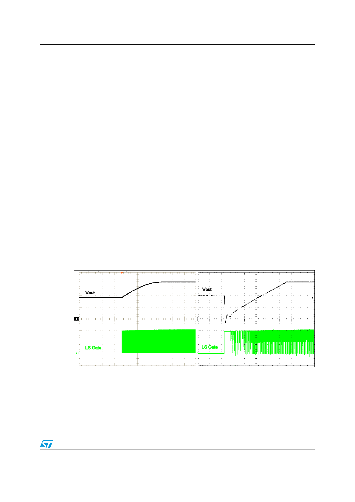
In order to avoid any kind of negative undershoot and dangerous return from the load during
start-up, L6728AH performs a special sequence in enabling LS driver to switch: during the
soft-start phase, the LS driver results disabled (LS = OFF) until the HS starts to switch. This
avoid the dangerous negative spike on the output voltage that can happen if starting over a
pre-biased output.
If the output voltage is pre-biased to a voltage higher than the final one, the HS would never
start to switch. In this case, at the end of soft-start time, LS is enabled and discharge the
output to the final regulation value.
This particular feature of the device masks the LS turn-on only from the control loop point of
view: protections by-pass this turning ON the LS MOSFET in case of need.
Figure 4. LSLess startup (left) vs. non-LSLess startup (right)
V
power supply is above UVLO threshold
CC
Doc ID 15726 Rev 1 11/33
Page 12

Over-current protection L6728AH
7 Over-current protection
The over-current function protects the converter from a shorted output or overload, by
sensing the output current information across the low side MOSFET drain-source onresistance, R
avoiding the use of expensive and space-consuming sense resistors.
. This method reduces cost and enhances converter efficiency by
DS(on)
The low side R
current sense is implemented by comparing the voltage at the PHASE
DS(on)
node when LS MOSFET is turned on with the programmed OCP thresholds voltages,
internally held. If the monitored voltage is bigger than these thresholds, an over-current
event is detected.
For maximum safety and load protection, L6728AH implements a dual level over-current
protection system:
st
● 1
level threshold: it is the user externally set threshold. If the monitored voltage on
PHASE exceeds this threshold, a 1
st
level over-current is detected. If four 1st level OC
events are detected in four consecutive switching cycles, over-current protection will be
triggered.
nd
● 2
level threshold: it is an internal threshold whose value is equal to 1st level
threshold multiplied by a factor 1.5. If the monitored voltage on PHASE exceeds this
threshold, over-current protection will be triggered immediately.
When over-current protection is triggered, the device turns off both LS and HS MOSFETs in
a latched condition. To recover from over-current protection triggered condition, V
supply must be cycled.
7.1 Over-current threshold setting
L6728AH allows to easily program a 1st level over-current threshold ranging from 50 mV to
550 mV, simply by adding a resistor (R
will be automatically set accordingly.
OCSET
power
CC
) between LGATE and GND. 2nd level threshold
During a short period of time (about 5 ms) following
internal 10 µA current (I
across R
. This voltage drop will be sampled and internally held by the device as 1st
OCSET
) is sourced from LGATE pin, determining a voltage drop
OCSET
level over-current threshold. The OC setting procedure overall time length is about 5 ms.
Connecting a R
resistor between LGATE and GND, the programmed 1st level
OCSET
threshold will be:
I
OCth1
the programmed 2
In case R
OCSET
nd
level threshold will be:
I
OCth2
is not connected, the device sets the OCP thresholds to the maximum
values: an internal safety clamp on LGATE is triggered as soon as LGATE voltage reaches
600 mV, setting the maximum threshold and suddenly ending OC setting phase.
12/33 Doc ID 15726 Rev 1
V
I
OCSETROCSET
------------------------------------------- -=
1.5
⋅=
⋅
R
dsON
I
OCSETROCSET
------------------------------------------- -
R
dsON
rising over UVLO threshold, an
CC
⋅
Page 13

L6728AH Output voltage setting and protections
8 Output voltage setting and protections
L6728AH is capable to precisely regulate an output voltage as low as 0.8 V. In fact, the
device comes with a fixed 0.8 V internal reference that guarantee the output regulated
voltage to be within ±1% tolerance over line and temperature variations (excluding output
resistor divider tolerance, when present).
Output voltage higher than 0.8 V can be easily achieved by adding a resistor R
between
OS
FB pin and ground. Referring to Figure 1, the steady state DC output voltage will be:
R
FB
1
-----------+
R
OS
where V
REF
is 0.8 V.
V
OUT
V
⎛⎞
⋅=
REF
⎝⎠
L6728AH monitors the voltage at VSEN pin and compares it to internal reference voltage in
order to provide under voltage and overvoltage protections as well as PGOOD signal.
According to the level of VSEN, different actions are performed from the controller:
● PGOOD
If the voltage monitored through VSEN exits from the PGOOD window limits, the device
de-asserts the PGOOD signal still continuing switching and regulating. PGOOD is
asserted at the end of the soft-start phase.
● Under voltage protection
If the voltage at VSEN pin drops below UV threshold, the device turns off both HS and
LS MOSFETs, latching the condition. Cycle V
● Overvoltage protection
to recover.
CC
If the voltage at VSEN pin rises over OV threshold (1 V typ), overvoltage protection
turns off HS MOSFET and turns on LS MOSFET. The LS MOSFET will be turned off as
soon as VSEN goes below V
/2 (0.4 V). The condition is latched, cycle VCC to
REF
recover. Notice that, even if the device is latched, the device still controls the LS
MOSFET and can switch it on whenever VSEN rises above 0.4 V.
● Feedback disconnection protection
In order to provide load protection even if VSEN pin is not connected, a 100 nA bias
current is always sourced from this pin. If VSEN pin is not connected, this current will
permanently pull it up causing the device to detect an OV: thus LS will be latched on
preventing output voltage from rising out of control.
Doc ID 15726 Rev 1 13/33
Page 14
Application details L6728AH
9 Application details
9.1 Compensation network
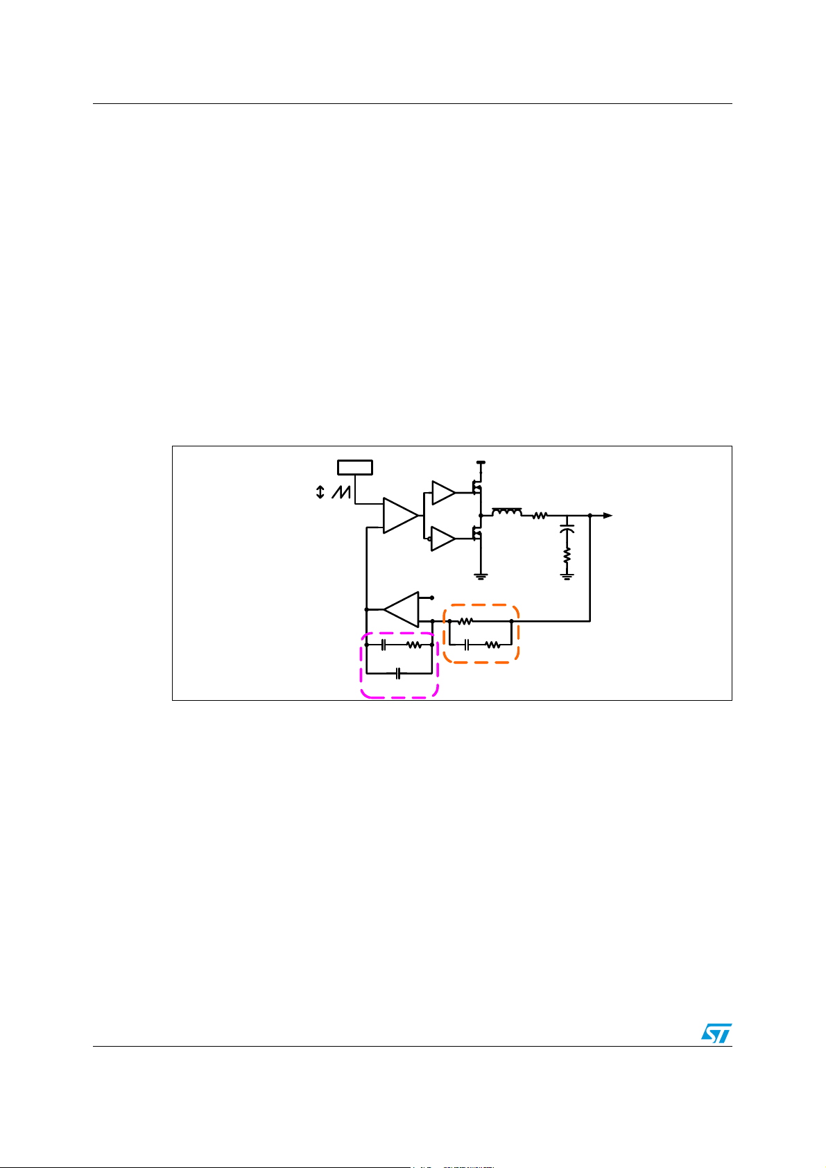
The control loop showed in Figure 5 is a voltage mode control loop. The output voltage is
regulated to the internal reference (when present, offset resistor between FB node and GND
can be neglected in control loop calculation).
Error amplifier output is compared to oscillator saw-tooth waveform to provide PWM signal
to the driver section. PWM signal is then transferred to the switching node with V
amplitude. This waveform is filtered by the output filter.
The converter transfer function is the small signal transfer function between the output of the
EA and V
filter and a zero at F
modulator is simply the input voltage V
ΔV
OSC
. This function has a double pole at frequency FLC depending on the L-C output
OUT
depending on the output capacitor ESR. The DC gain of the
ESR
divided by the peak-to-peak oscillator voltage
IN
.
Figure 5. PWM control loop
V
OSC
ΔV
OSC
_
+
PWM
COMPARATOR
ERROR
AMPLIFIER
+
_
V
REF
IN
L R
C
OUT
ESR
R
FB
V
OUT
IN
C
F
C
The compensation network closes the loop joining V
function ideally equal to -Z
F/ZFB
.
Compensation goal is to close the control loop assuring high DC regulation accuracy, good
dynamic performances and stability. To achieve this, the overall loop needs high DC gain,
high bandwidth and good phase margin.
High DC gain is achieved giving an integrator shape to compensation network transfer
function. Loop bandwidth (F
stability, it should not exceed F
) can be fixed choosing the right RF/RFB ratio, however, for
0dB
/2π. To achieve a good phase margin, the control loop gain
SW
has to cross 0 dB axis with -20 dB/decade slope.
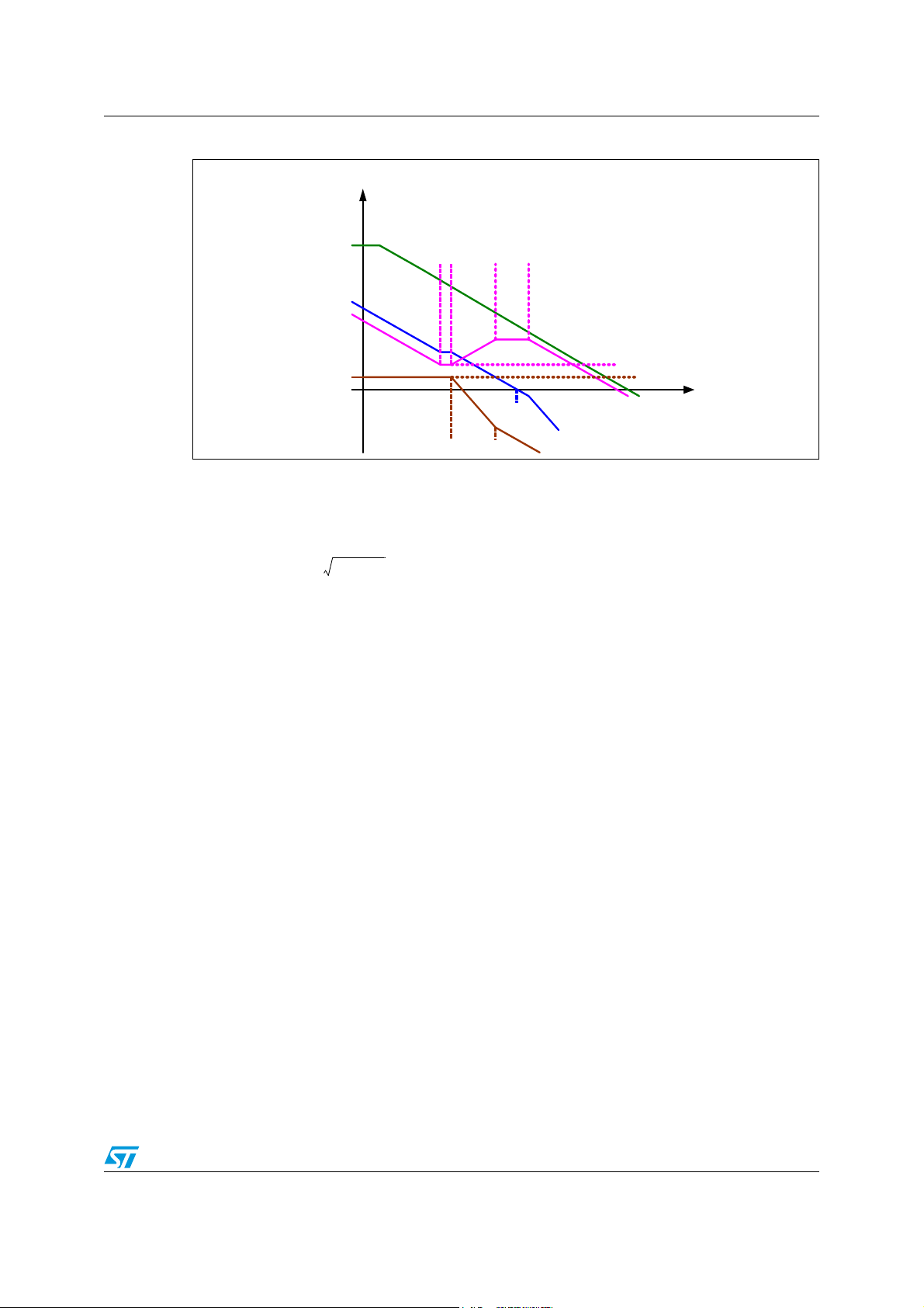
As an example, Figure 6 shows an asymptotic bode plot of a type III compensation.
14/33 Doc ID 15726 Rev 1
R
F
P
C
R
S
S
Z
Z
F
FB
and EA output with transfer
OUT
Page 15
L6728AH Application details
Figure 6. Example of type III compensation
Gain
[dB]
open loop
EA gain
FZ1F
Z2FP1FP2
closed
loop ga in
compensation
gain
open loop
converter gain
0dB
● Open loop converter singularities:
F
LCFESR
F
0dB
20 log ( RF/RFB)
20log (V
/ΔV
IN
Log (Fre q)
OSC
)
a)
b)
F
F
LC
ESR
1
--------------------------------- -=
2π LC
⋅
------------------------------------------- -=
2π C
OUT
OUT
1
ESR⋅⋅
● Compensation network singularities frequencies:
a)
b)
c)
d)
F
Z1
F
Z2
F
P1
F
P2
1
------------------------------=
⋅⋅
2π R
FCF
---------------------------------------------------- -=
2π R
--------------------------------------------------=
2π R
------------------------------ -=
2π RSC
1
+()C
⋅⋅
FBRS
S
1
CFCP⋅
⎛⎞
-------------------- -
⋅⋅
F
⎝⎠
C
+
FCP
1
⋅⋅
S
To place the poles and zeroes of the compensation network, the following suggestions may
be followed:
a) Set the gain R
according to the approximated formula (suggested values for R
in order to obtain the desired closed loop regulator bandwidth
F/RFB
is in the range of
FB
some kΩ):
ΔV
F
R
----------
R
FB
0dB
F
------------
F
LC
------------------ -
⋅=
V
OSC
IN
Doc ID 15726 Rev 1 15/33
Page 16

Application details L6728AH
b) Place FZ1 below FLC (typically 0.5*FLC):
1
-----------------------------=
C
F
⋅⋅
π R
FFLC
c) Place F
C
P
d) Place F
R
S
C
S
at F
P1
ESR
----------------------------------------------------------=
2π RFCFF
Z2
---------------------------=
F
----------------- - 1–
2F⋅
-------------------------------=
⋅⋅
π R
C
at FLC and FP2 at half of the switching frequency:
R
FB
SW
LC
1
SFSW
e) Check that compensation network gain is lower than open loop EA gain before
;
F
0dB
f) Check phase margin obtained (it should be greater than 45°) and repeat if
necessary.
9.2 Layout guidelines
L6728AH provides control functions and high current integrated drivers to implement highcurrent step-down DC-DC converters. In this kind of application, a good layout is very
important.
The first priority when placing components for these applications has to be reserved to the
power section, minimizing the length of each connection and loop as much as possible. To
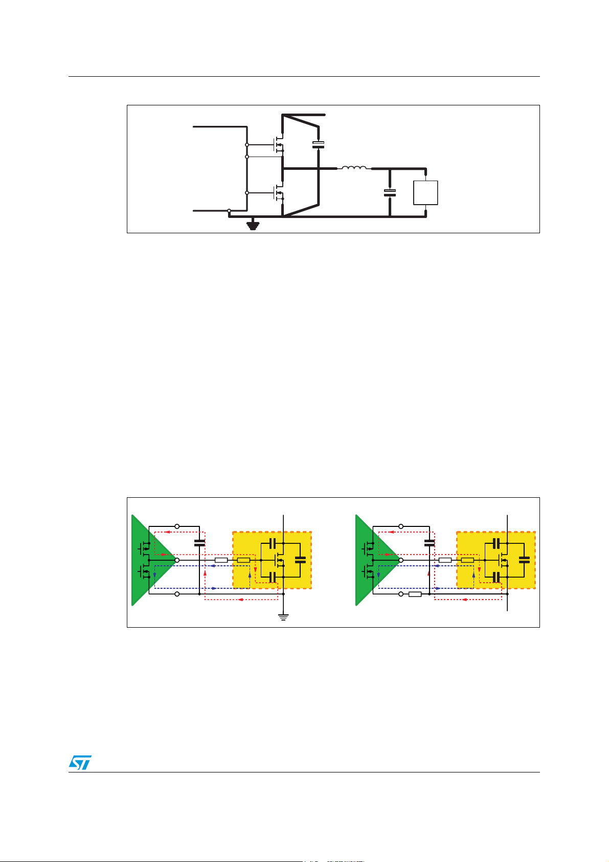
minimize noise and voltage spikes (EMI and losses) power connections (highlighted in
Figure 7) must be a part of a power plane and anyway realized by wide and thick copper
traces: loop must be anyway minimized. The critical components, i.e. the power MOSFETs,
must be close one to the other. The use of multi-layer printed circuit board is recommended.
:
F
1–⋅⋅⋅
ESR
The input capacitance (C
), or at least a portion of the total capacitance needed, has to be
IN
placed close to the power section in order to eliminate the stray inductance generated by the
copper traces. Low ESR and ESL capacitors are preferred, MLCC are suggested to be
connected near the HS drain.
Use proper VIAs number when power traces have to move between different planes on the
PCB in order to reduce both parasitic resistance and inductance. Moreover, reproducing the
same high-current trace on more than one PCB layer will reduce the parasitic resistance
associated to that connection.
Connect output bulk capacitors (C
OUT
inductance and resistance associated to the copper trace, also adding extra decoupling
16/33 Doc ID 15726 Rev 1
capacitors along the way to the load when this results in being far from the bulk capacitors
bank.
) as near as possible to the load, minimizing parasitic
Page 17
L6728AH Application details
Figure 7. Power connections (heavy lines)
V
IN
UGATE
PHASE
L6728A
L6728AH
LGATE
GND
C
IN
L
C
OUT
LOAD
Gate traces and phase trace must be sized according to the driver RMS current delivered to
the power MOSFET. The device robustness allows managing applications with the power
section far from the controller without losing performances. Anyway, when possible, it is
recommended to minimize the distance between controller and power section.
Small signal components and connections to critical nodes of the application, as well as
bypass capacitors for the device supply, are also important. Locate bypass capacitor (V
CC
and Bootstrap capacitor) and feedback compensation components as close to the device as
practical. For over current programmability, place R
close to the device and avoid
OCSET
leakage current paths on COMP/OC pin, since the internal current source is only 60 μA.
Systems that do not use Schottky diode in parallel to the low-side MOSFET might show big
negative spikes on the phase pin. This spike must be limited within the absolute maximum
ratings (for example, adding a gate resistor in series to HS MOSFET gate), as well as the
positive spike, but has an additional consequence: it causes the bootstrap capacitor to be
over-charged. This extra-charge can cause, in the worst case condition of maximum input
voltage and during particular transients, that boot-to-phase voltage overcomes the absolute
maximum ratings also causing device failures. It is then suggested in this cases to limit this
extra-charge by adding a small resistor in series to the boot capacitor (one resistor in series
to BOOT).
Figure 8. Drivers turn-on and turn-off paths
LS DRIVER LS MOSFET
VCC
C
GD
R
GATERINT
LGATE
C
GS
GND
C
DS
Doc ID 15726 Rev 1 17/33
HS DRIVER HS MOSFET
BOOT
C
GD
R
GATERINT
UGATE
C
GS
PHASE
C
DS
Page 18

Application information L6728AH
10 Application information
10.1 Inductor design
The inductance value is defined by a compromise between the dynamic response time, the
efficiency, the cost and the size. The inductor has to be calculated to maintain the ripple
current (ΔI
value can be calculated with the following relationship:
) between 20% and 30% of the maximum output current (typ.). The inductance
L
⋅
OUT
V
--------------
⋅=
OUT
V
IN
is the output
OUT
where F
VINV
–
----------------------------- -
L
F
SWΔIL
is the switching frequency, VIN is the input voltage and V
SW
voltage.
Increasing the value of the inductance reduces the current ripple but, at the same time,
increases the converter response time to a dynamic load change. The response time is the
time required by the inductor to change its current from initial to final value. Until the inductor
has not finished its charging time, the output current is supplied by the output capacitors.
Minimizing the response time can minimize the output capacitance required. If the
compensation network is well designed, during a load variation the device is able to set a
duty cycle value very different (0% or 80%) from steady state one. When this condition is
reached, the response time is limited by the time required to change the inductor current.
18/33 Doc ID 15726 Rev 1
Page 19

L6728AH Application information
10.2 Output capacitor(s)
The output capacitors are basic components to define the ripple voltage across the output
and for the fast transient response of the power supply. They depend on the output voltage
ripple requirements, as well as any output voltage deviation requirement during a load
transient.
During steady-state conditions, the output voltage ripple is influenced by both the ESR and
capacitive value of the output capacitors as follow:
Where ΔI
ΔV
OUT_ESR
ΔV
OUT_C
is the inductor current ripple. In particular, the expression that defines ΔV
L
ΔILESR⋅=
-------------------------------------- -
ΔI
⋅=
L
8C
⋅⋅
1
OUTFSW
OUT_C
takes in consideration the output capacitor charge and discharge as a consequence of the
inductor current ripple.
During a load variation, the output capacitors supplies the current to the load or absorb the
current stored into the inductor until the converter reacts. In fact, even if the controller
recognizes immediately the load transient and sets the duty cycle at 80% or 0%, the current
slope is limited by the inductor value. The output voltage has a drop that also in this case
depends on the ESR and capacitive charge/discharge as follow:
ΔV
OUT_ESR
ΔV
OUT_C
Where ΔV
D
( for the load appliance or V
MAXVINVOUT
is the voltage applied to the inductor during the transient response
L
–⋅
ΔI
OUT
ΔI
OUT
ESR⋅=
OUT
L ΔI
⋅
------------------------------------- -
⋅=
2C
OUT
⋅⋅
OUTΔVL
for the load removal).
MLCC capacitors have typically low ESR to minimize the ripple but also have low
capacitance that do not minimize the voltage deviation during dynamic load variations. On
the contrary, electrolytic capacitors have big capacitance to minimize voltage deviation
during load transients while they does not show the same ESR values of the MLCC resulting
then in higher ripple voltages. For these reasons, a mix between electrolytic and MLCC
capacitor is suggested to minimize ripple as well as reducing voltage deviation in dynamic
mode.
10.3 Input capacitors
The input capacitor bank is designed considering mainly the input RMS current that
depends on the output deliverable current (I
follow:
The equation reaches its maximum value, I
input capacitor ESR and, in worst case, are:
) and the duty-cycle (D) for the regulation as
OUT
I
rmsIOUT
PESRI
D1D–()⋅⋅=
/2, with D = 0.5. The losses depends on the
OUT
2
OUT
2⁄()
⋅=
Doc ID 15726 Rev 1 19/33
Page 20
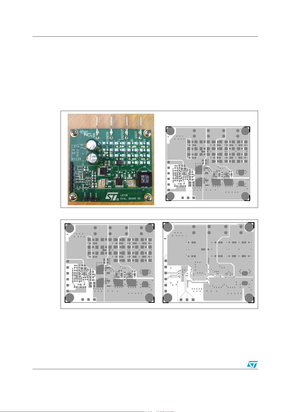
20 A demonstration board L6728AH
11 20 A demonstration board
L6728AH 20 A demonstration board realizes, in a two-layer PCB, a step-down DC/DC
converter and shows the operation of the device in a general-purpose high-current
application. Different output voltage rails have been considered: 8 V, 5 V, 3.3 V, 2.5 V, 1.25 V
and 0.8 V. The input voltage can range from a bottom value that depends on the chosen rail
up to 15 V buses (absolute maximum). The application can deliver an output current up to
the value fixed by R
Figure 9. 20 A demonstration board (left) and components placement (right)
OCSET
(~27 A).
Figure 10. 20 A demonstration board’s top (left) and bottom (right) layers
20/33 Doc ID 15726 Rev 1
Page 21
L6728AH 20 A demonstration board
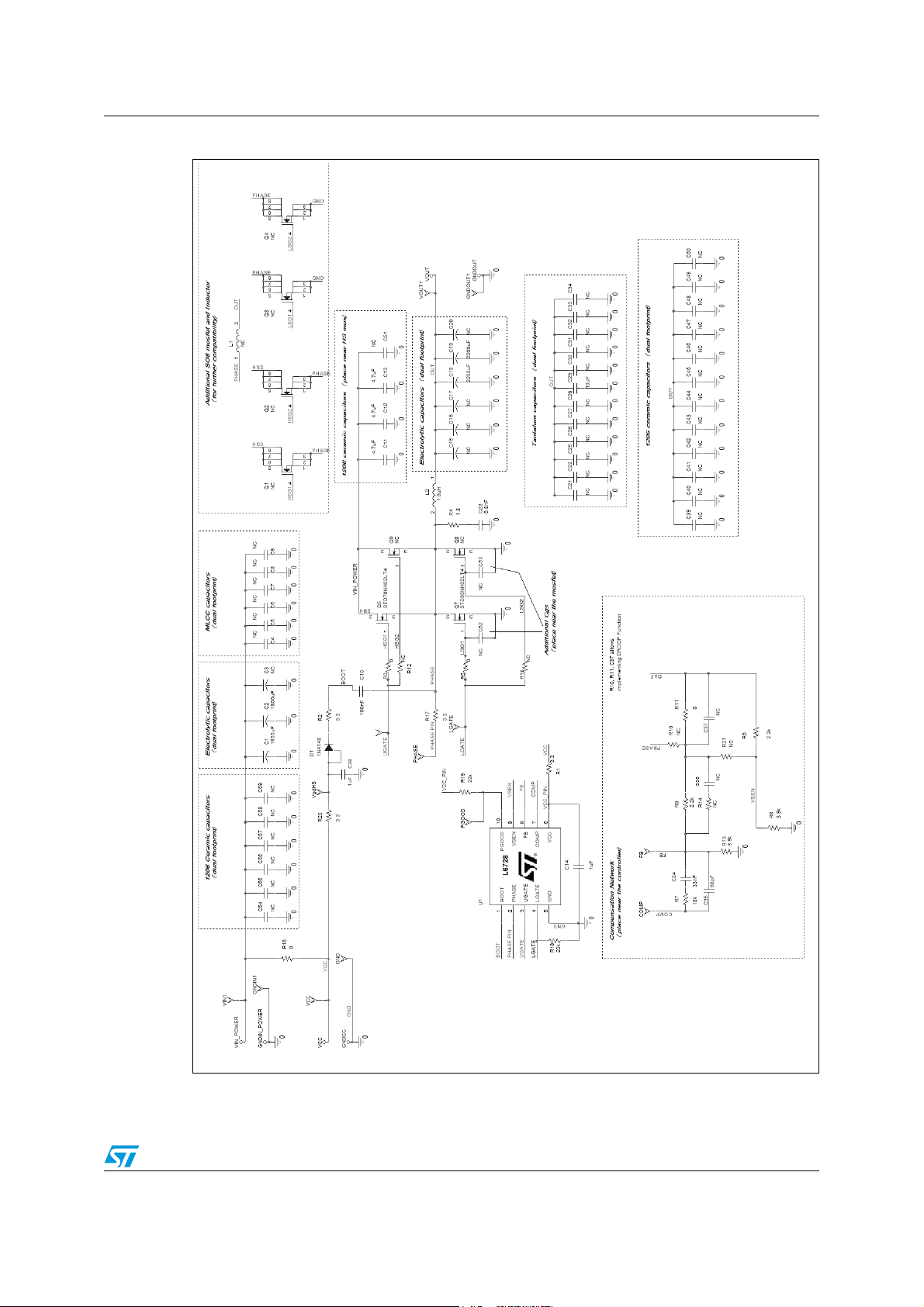
Figure 11. 20 A demonstration board schematic
Doc ID 15726 Rev 1 21/33
Page 22
20 A demonstration board L6728AH
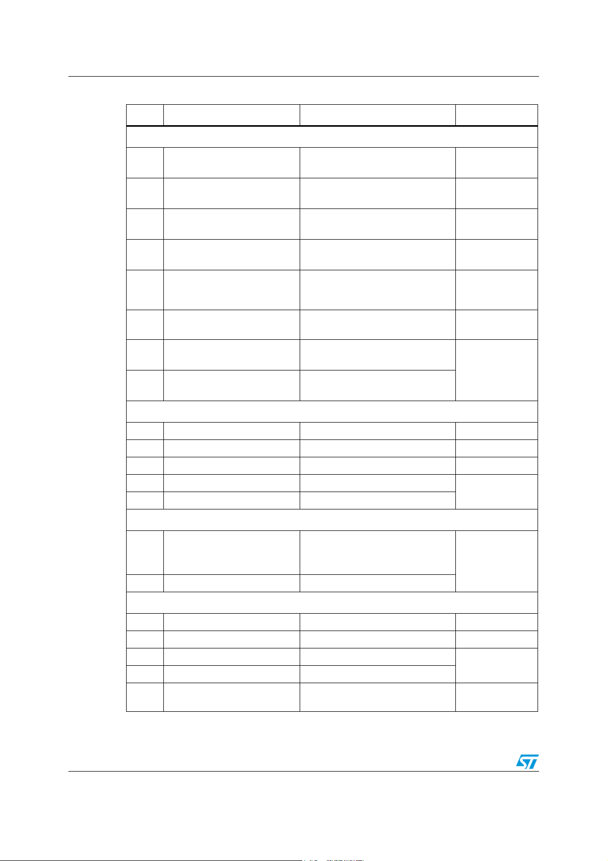
Table 6. 20A demonstration board - bill of material (common components)
Qty Reference Description Package
Capacitors
2C1, C2
1C10
3 C11 to C13
2C14, C38
Electrolytic capacitor 1800 μF 16 V
Sanyo P/N 16ME1800WG
MLCC, 100 nF, 50 V, X7R
Murata GRM188R71H104K
MLCC, 4.7 μF, 1 6 V, X 7 R
Murata GRM31CR71C475K
MLCC, 1 μF, 1 6 V, X 7 R
Murata GRM21BR71C105K
Radial 10 x 23 mm
SMD0603
SMD1206
SMD0805
C3 to C9, C15 to C20, C39 to
48
C59, C36, C37, C21 to C23,
Not mounted N.A.
C25 to C29, C31 to C34
1C30
1C24
POSCAP 470 μF, 6.3 V, 10 mΩ
Sanyo P/N 6TPD470M
MLCC, 47 nF, 50 V, X7R
Murata GRM188R71H473K
SMD1206
SMD0603
1C35
MLCC, 100 pF, 50 V, X7R
Murata GRM188R71H101K
Resistors
4 R1, R2, R20, R17 Resistor, 2R2, 1/16W, 1% SMD0603
5 R3, R5, R11, R12, R16 Resistor, 0R, 1/8W, 1% SMD0805
5 R4, R10, R14, R15, R21 Not mounted N.A.
1 R19 Resistor, 22 K, 1/16W, 1%
SMD0603
1 R18 Resistor, 18 K, 1/16W, 1%
Inductor
1L1
1L2 Not mounted
Active components
1 D1 Diode, 1N4148 SOT23
5 Q1 to Q4, Q8 Not mounted N.A.
1 Q5 STD70NH02L
1 Q7 STD95NH02L
1 U1 Controller, L6728AH
22/33 Doc ID 15726 Rev 1
Wurth SMD power inductor
670 nH - 1.75 mΩ - 40 A
P/N 744-315-067
N.A.
DPACK
VFQFPN10,
3x3 mm
Page 23
L6728AH 20 A demonstration board
11.1 Demonstration board description
11.1.1 Power input (VIN)
This is the input voltage for the power conversion. The high-side drain is connected to this
input. This voltage can range from 1.5 V to 12 V bus.
If the voltage is between 5 V and 12 V it can supply also the device (through the V
and in this case the R16 (0 Ω) resistor must be present.
11.1.2 Output (V
OUT
)
Different output voltage rails have been tested. For each rail a few component need to be
changed: these components are used to program the desiderated output voltage and to
compensate the system. The over-current-protection limit is set to ~27 A but it can be
changed by replacing the resistors R18.
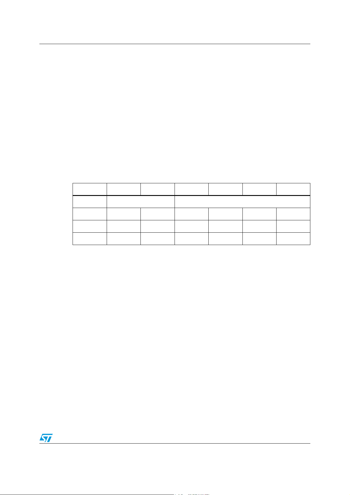
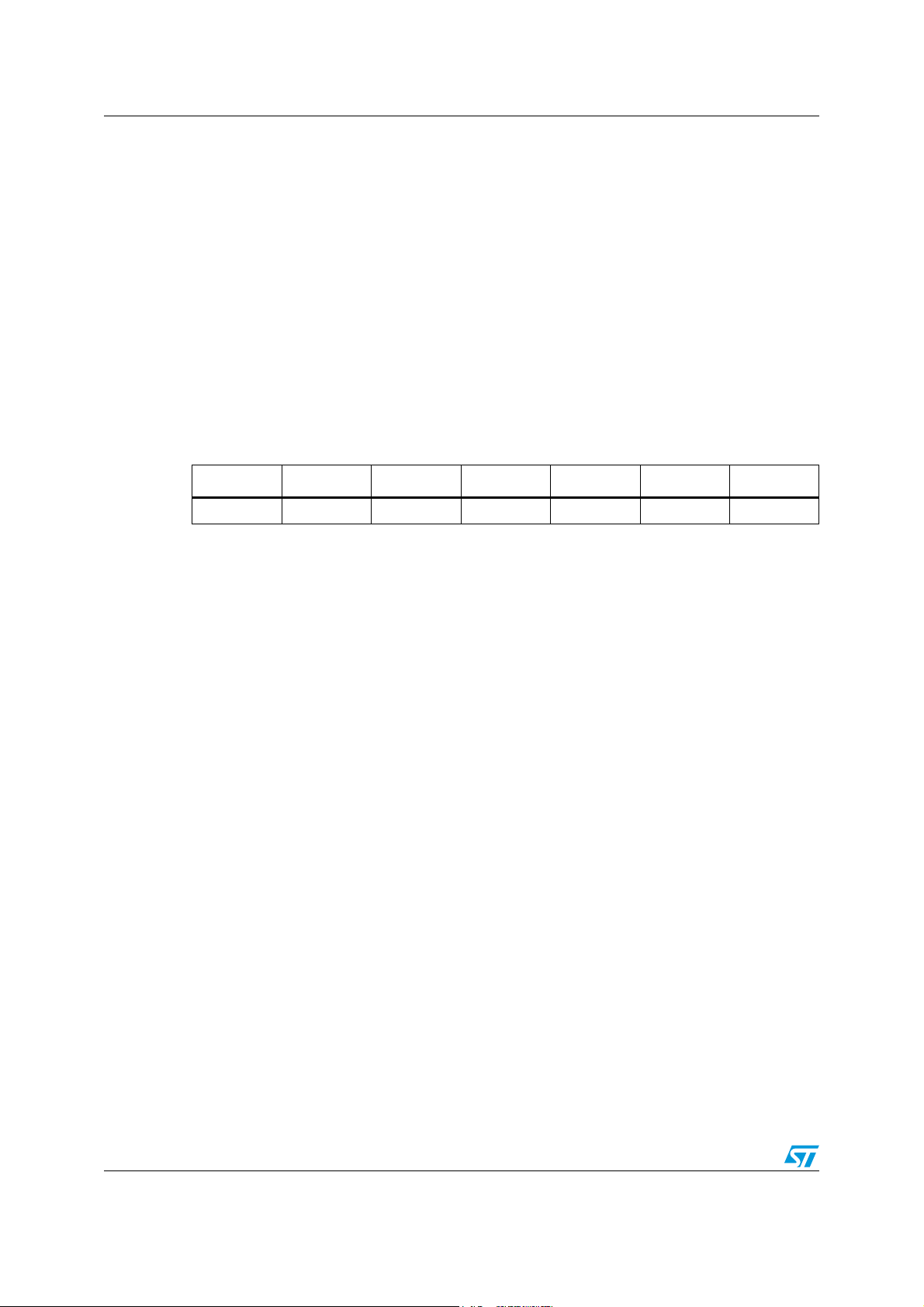
Table 7. Rail dependent components
Ref. 8 V rail 5 V rail 3.3 V rail 2.5 V rail 1.25 V rail 0.8 V rail
Q9 Mounted Not mounted
R7 3.6 kΩ 3.6 kΩ 3.6 kΩ 3.6 kΩ 11 kΩ 11 kΩ
R6, R9 3.6 kΩ 3.6 kΩ 4.7 kΩ 4.7 kΩ 22 kΩ 22 kΩ
R8, R13 390 Ω 680 Ω 1.5 kΩ 2.2 kΩ 39 kΩ Open
Note: All the previous resistors are SMD 0603 package, 1/16W, 1% tolerance.
11.1.3 Signal input (VCC)
CC
pin)
Using the input voltage VIN to supply the controller no power is required at this input.
However the controller can be supplied separately from the power stage through the V
input and, in this case, the R16 (0 Ω) resistor must be unsoldered.
11.1.4 Test points
Several test points are provided to have easy access at all important signal characterizing
the device:
– COMP: The output of the error amplifier;
– FB: The inverting input of the error amplifier;
– PGOOD: Signaling the regular functioning (active high);
– VGDHS: The bootstrap diode anode;
– PHASE: Phase node;
– LGATE: Low-side gate pin of the device;
– HGATE: High-side gate pin of the device.
Doc ID 15726 Rev 1 23/33
CC
Page 24
20 A demonstration board L6728AH
11.2 Demonstration board characterization
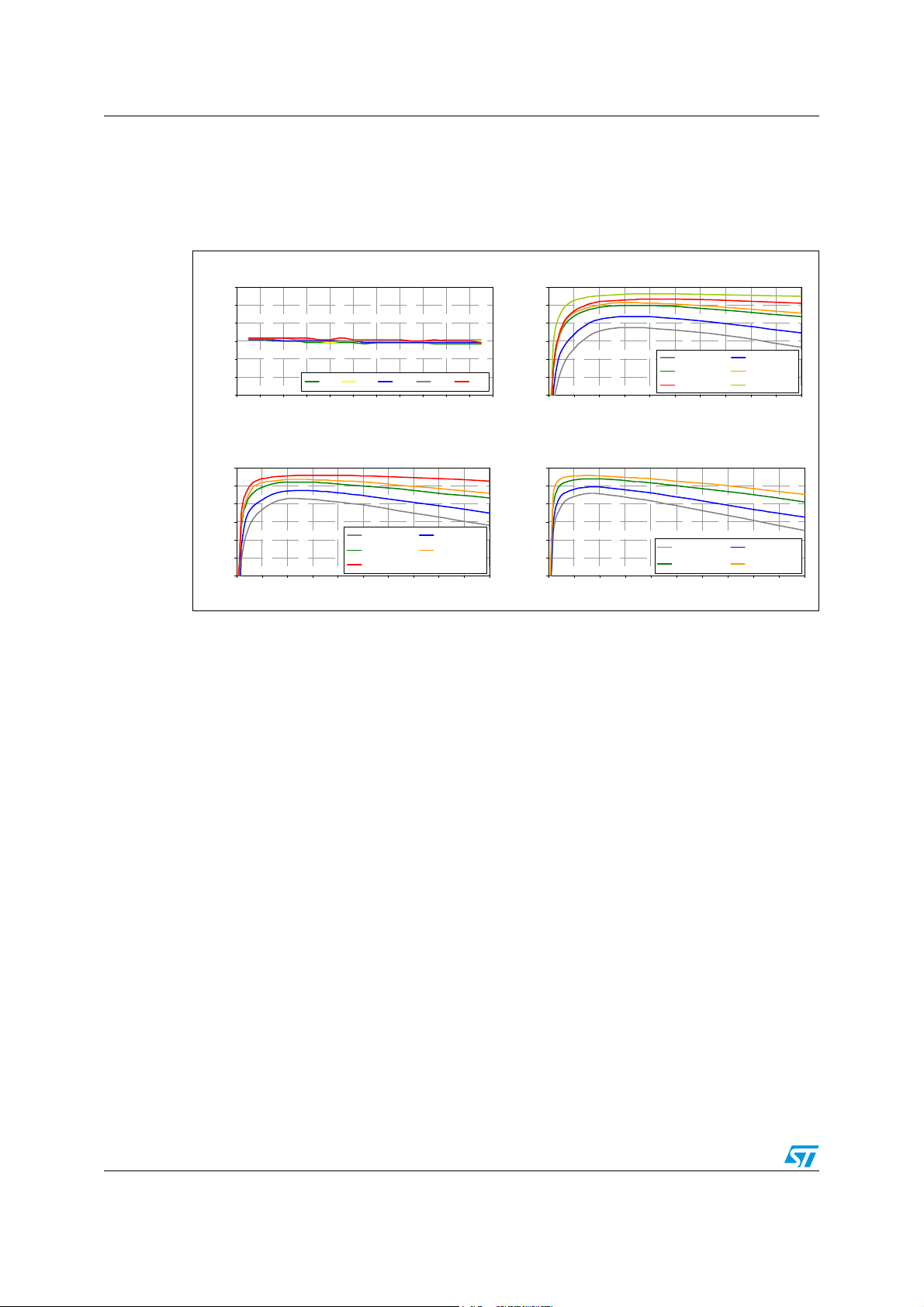
Figure 12 and Figure 17 show the electrical performances of the tamboured in terms of
accuracy and efficiency.
Figure 12. 20 A demonstration board performances
Load / Line Regulation
0,3%
0,2%
0,1%
0,0%
-0,1%
-0,2%
Output Voltage Error [%]
-0,3%
4 5 6 7 8 9 10 11 12 13 14 15
0A 5A 10A 15A 20A
Input Voltage [V]
Input Voltage @ 8 V
100%
90%
80%
70%
60%
Efficiency [%]
50%
40%
0,0 2,5 5,0 7,5 10,0 12,5 15,0 17,5 20,0 22,5 25,0
Vout = 0. 8 V Vout = 1.25 V
Vout = 2. 5 V Vout = 3.3 V
Vout = 5 V
Output Current [A]
100%
90%
80%
70%
60%
Efficiency [%]
50%
40%
0,0 2,5 5,0 7,5 10,0 12,5 15,0 17,5 20,0 22,5 25,0
100%
90%
80%
70%
60%
Efficiency [%]
50%
40%
0 3 5 8 10 13 15 18 20 23 25
Input Voltage @ 12 V
Vout = 0. 8 V Vout = 1.25 V
Vout = 2. 5 V Vout = 3.3 V
Vout = 5 V Vout = 8 V
Output Current [A]
Input Voltage @ 5 V
Vout = 0.8 V Vout = 1. 25 V
Vout = 2.5 V Vout = 3. 3 V
Output Current [A]
24/33 Doc ID 15726 Rev 1
Page 25
L6728AH 5 A demonstration board
12 5 A demonstration board
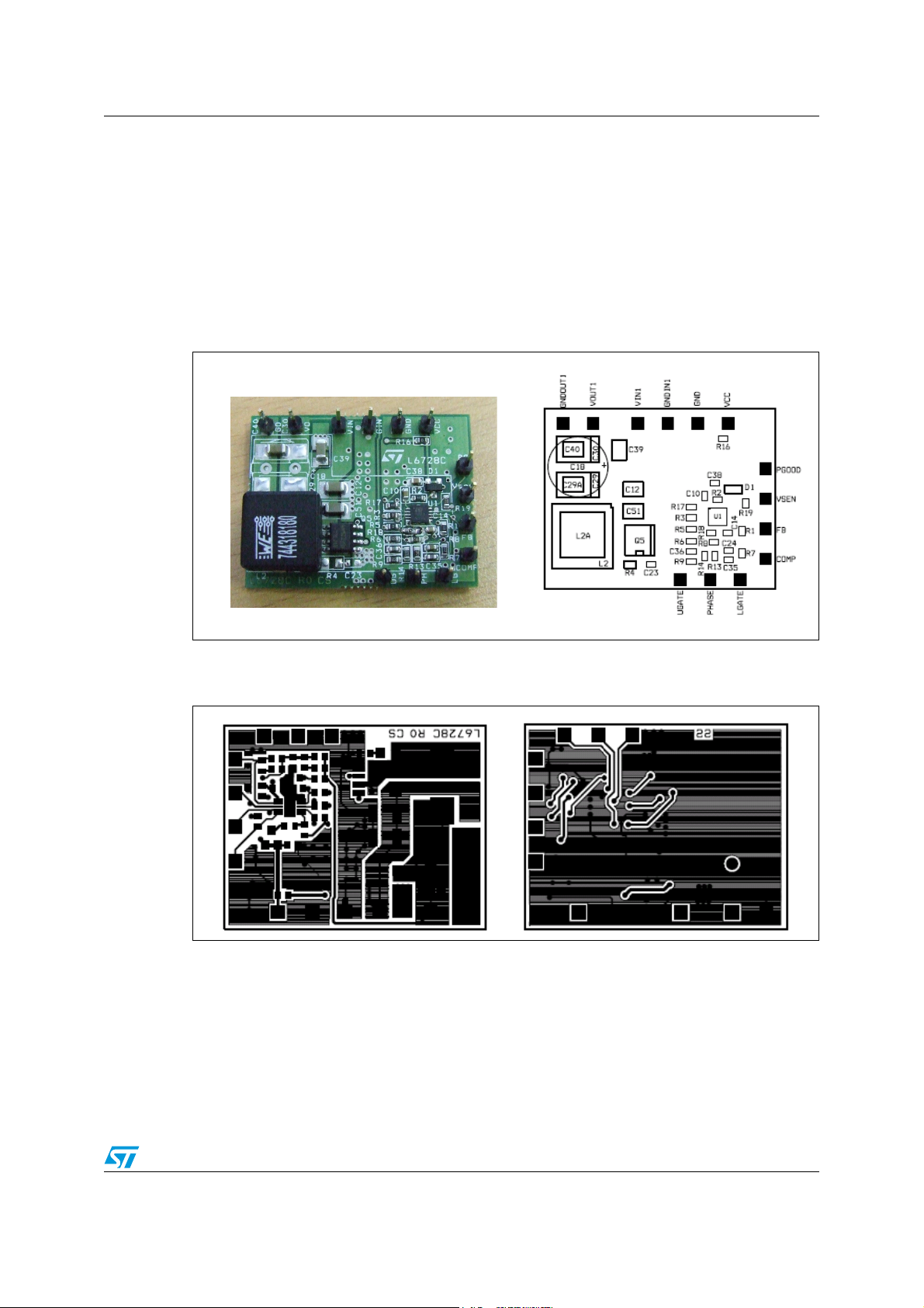
L6728AH 5 A demonstration board realizes, in a two-layer PCB, a step-down DC/DC
converter and shows the operation of the device in a general-purpose high-current
application. Different output voltage rails have been considered: 8 V, 5 V, 3.3 V, 2.5 V, 1.25 V
and 0.8 V. The input voltage can range from a bottom value that depends on the chosen rail
up to 15 V buses (absolute maximum). The application can deliver an output current up to
the value fixed by R
Figure 13. 5 A demonstration board (left) and components placement (right)
OCSET
(~6 A).
Figure 14. 5 A demonstration board’s top (left) and bottom (right) layers
Doc ID 15726 Rev 1 25/33
Page 26
5 A demonstration board L6728AH
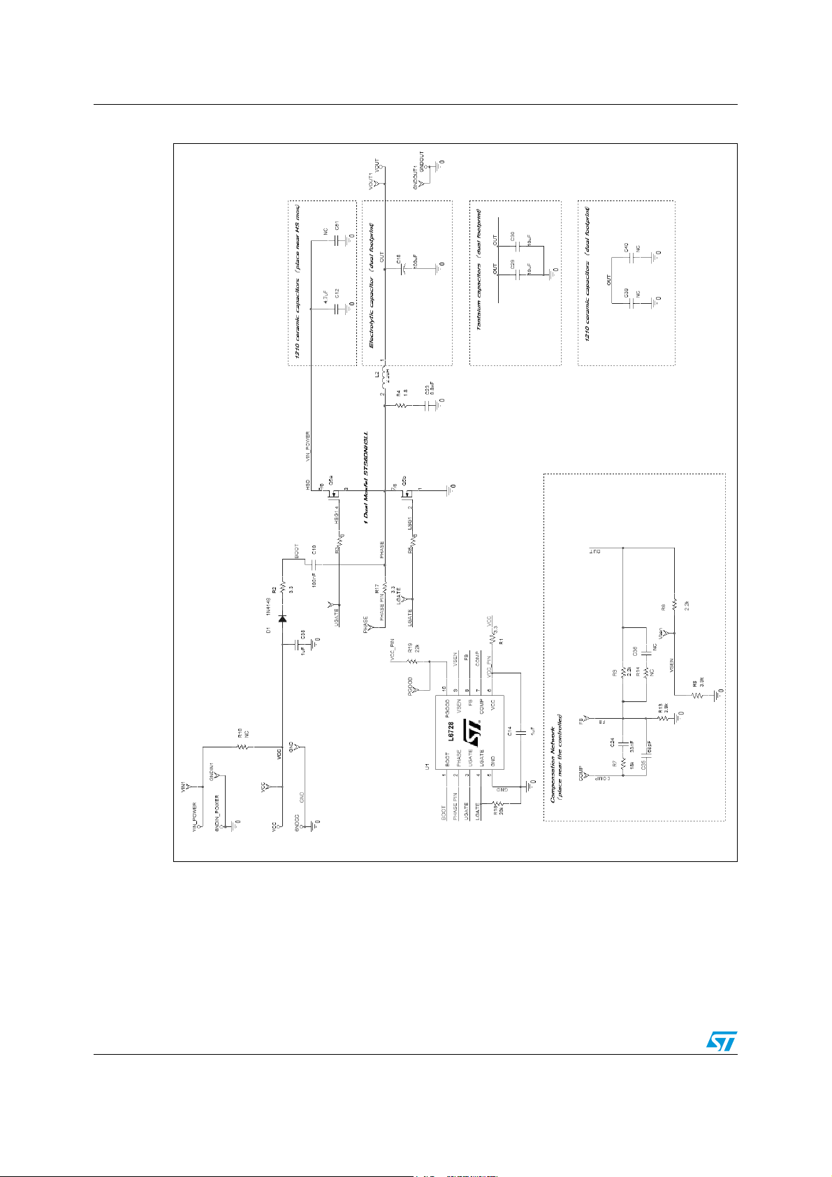
Figure 15. 5 A demonstration board schematic
26/33 Doc ID 15726 Rev 1
Page 27
L6728AH 5 A demonstration board
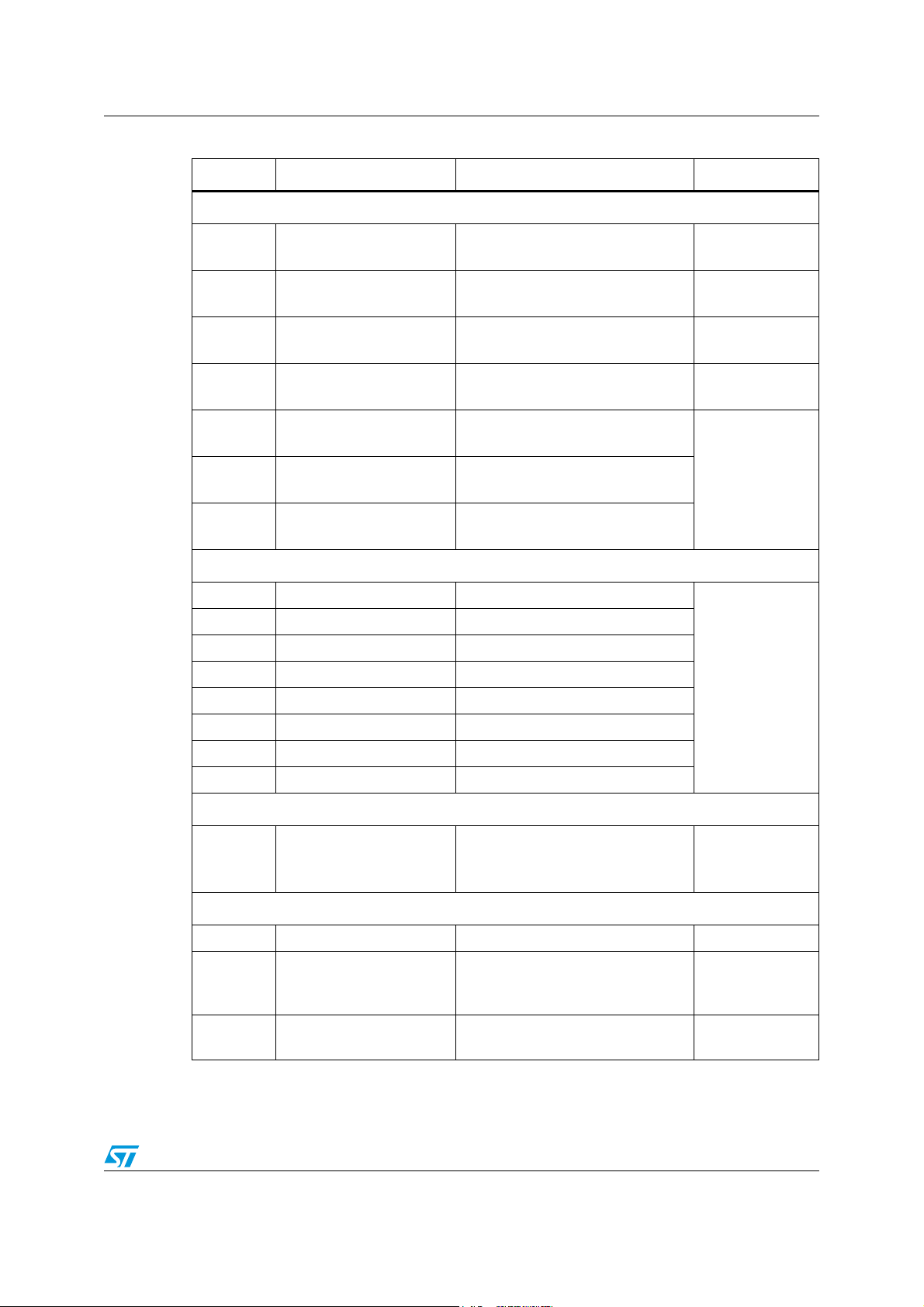
Table 8. 5 A demonstration board - bill of material
Qty Reference Description Package
Capacitors
2C12, C51
1C10
2C14, C38
2C39, C40
2C36
MLCC, 10 μF, 1 6 V, X5 R
Murata GRM31CR61C106K
MLCC, 100 nF, 50 V, X7R
Murata GRM188R71H104K
MLCC, 1 μF, 1 6 V, X 7 R
Murata GRM21BR71C105K
MLCC, 22 μF, 6.3 V, X5R
Murata GRM31CR60J226K
MLCC, 10 nF, 50 V, X7R
Murata GRM188R71H103K
MLCC, 47 nF, 50 V, X7R
Murata GRM188R71H223K
1C35
MLCC, 1 nF, 50 V, X7R
Murata GRM188R71H102K
Resistors
3 R1, R2, R17 Resistor, 3R3, 1/16 W, 1%
3 R3, R5, R16 Resistor, 0R, 1/8 W, 1%
1 R14 Resistor, 51R, 1/8 W, 1%
2 R6, R9 Resistor, 2K2, 1/16 W, 1%
2 R8, R13 Resistor, 3K9, 1/16 W, 1%
SMD1206
SMD0603
SMD0805
SMD1206
SMD06031C24
SMD0603
1 R7 Resistor, 270 R, 1/16 W, 1%
1 R19 Resistor, 22 K, 1/16 W, 1%
1 R18 Resistor, 18 K, 1/16 W, 1%
Inductor
Wurth SMD power inductor
1L1
1.8 μH - 3.68 mΩ - 20 A
N.A.
P/N 744-318-180
Active components
1 D1 Diode, BAT54 SOT23
Dual N-channel MOS,
1Q5
STS8DNF3LL (the STS8DNH3LL
SO8
model can be used as well)
1 U1 Controller, L6728AH
VFQFPN 10
3x3 mm
Doc ID 15726 Rev 1 27/33
Page 28
5 A demonstration board L6728AH
12.1 Demonstration board description
12.1.1 Power input (VIN)
This is the input voltage for the power conversion. The high-side drain is connected to this
input. This voltage can range from 1.5 V to 12 V bus.
If the voltage is between 5 V and 12 V it can supply also the device (through the Vcc pin)
and in this case the R16 (0 Ω) resistor must be present.
12.1.2 Output (V
OUT
)
Different output voltage rails have been tested. For each rail a few component need to be
changed: these components are used to program the desiderate output voltage. The OCP
limit is set to ~6 A but it can be changed by replacing the resistors R18.
Table 9. Rail dependent components
Ref. 8 V rail 5 V rail 3.3 V rail 2.5 V rail 1.25 V rail 0.8 V rail
R8, R13 240 Ω 430 Ω 680 Ω 1 kΩ 3.9 kΩ Open
Note: All the previous resistors are SMD 0603 package, 1/16W, 1% tolerance.
12.1.3 Signal input (VCC)
Using the input voltage VIN to supply the controller no power is required at this input.
However the controller can be supplied separately from the power stage through the V
input (5-12 V) and, in this case, the R16 (0 Ω) resistor must be unsoldered.
12.1.4 Test points
Several test points are provided to have easy access at all important signal characterizing
the device:
– COMP: The output of the error amplifier;
– FB: The inverting input of the error amplifier;
– PGOOD: Signaling the regular functioning (active high);
– VGDHS: The bootstrap diode anode;
– PHASE: Phase node;
– LGATE: Low-Side gate pin of the device;
– HGATE: High-Side gate pin of the device.
CC
28/33 Doc ID 15726 Rev 1
Page 29
L6728AH 5 A demonstration board
12.2 Demonstration board characterization
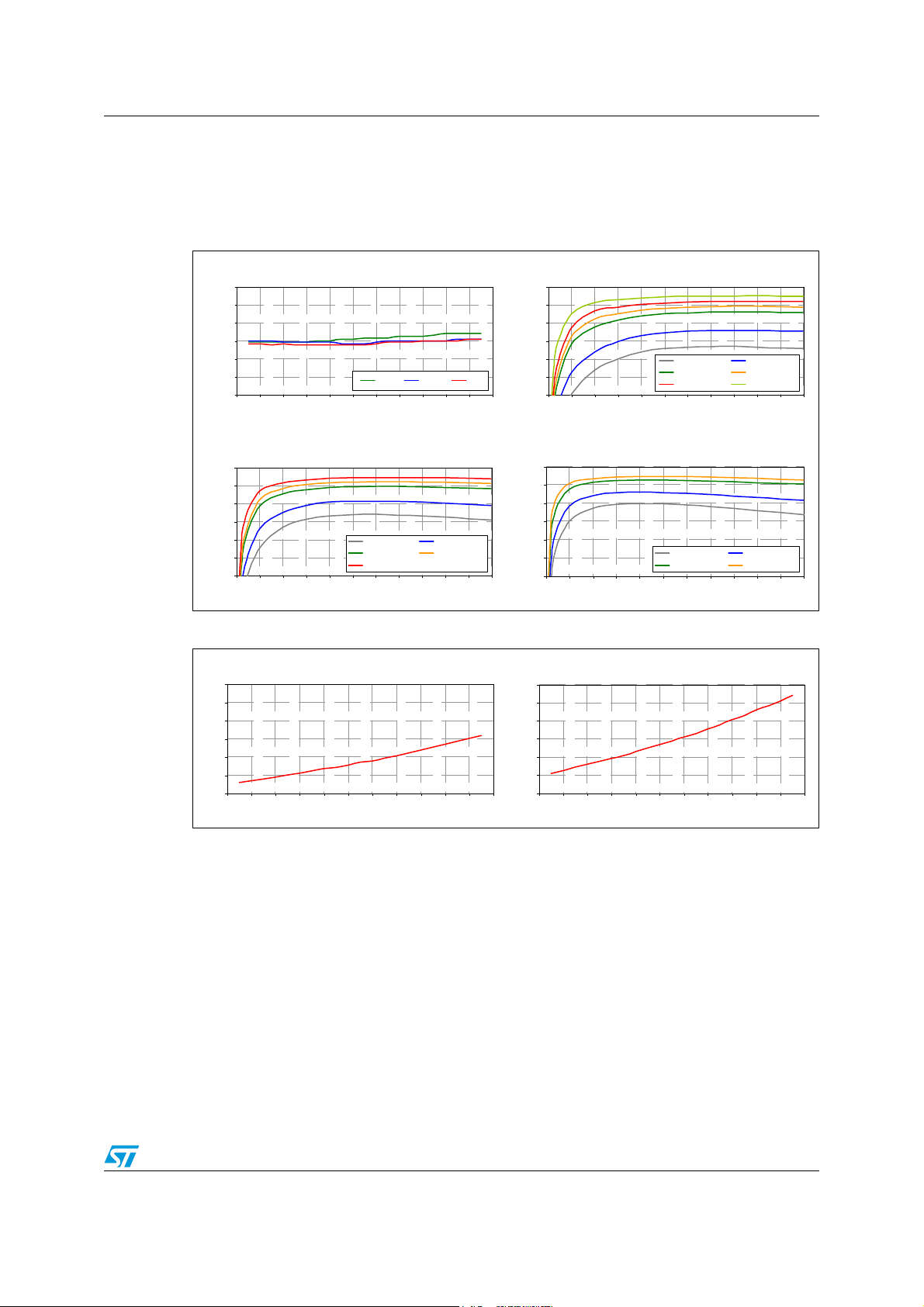
Figure 16 and Figure 17 show the electrical performances of the demonstration board in
terms of accuracy and efficiency.
Figure 16. 5 A demonstration board performances
Load / Line Regulation
0,3%
0,2%
0,1%
0,0%
-0,1%
-0,2%
Output Voltage Error [%]
-0,3%
4 5 6 7 8 9 10 11 12 13 14 15
0A 2. 5A 5A
Input Voltage [V]
Input Voltage @ 8 V
100%
90%
80%
70%
60%
Efficiency [%]
50%
40%
0,0 0,5 1,0 1,5 2,0 2,5 3,0 3,5 4,0 4,5 5,0 5,5
Vout = 0. 8 V Vout = 1.25 V
Vout = 2. 5 V Vout = 3.3 V
Vout = 5 V
Output Current [A]
100%
90%
80%
70%
60%
Efficiency [%]
50%
40%
0,0 0,5 1,0 1,5 2,0 2,5 3,0 3,5 4,0 4,5 5,0 5,5
100%
90%
80%
70%
60%
Efficiency [%]
50%
40%
0,0 0,5 1,0 1,5 2,0 2,5 3,0 3,5 4,0 4,5 5,0 5,5
Input Voltage @ 12 V
Vout = 0. 8 V Vout = 1.25 V
Vout = 2. 5 V Vout = 3.3 V
Vout = 5 V Vout = 8 V
Output Current [A]
Input Volt age @ 5 V
Vout = 0.8 V Vout = 1. 25 V
Vout = 2.5 V Vout = 3. 3 V
Output Current [A]
Figure 17. Demonstration boards power consumption @ 0 A output current
5A Demoboard Power Consumption
1,2
1,0
0,8
0,6
Power [W]
0,4
0,2
0,0
456789101112131415
1,2
1,0
0,8
0,6
Power [W]
0,4
0,2
0,0
4 5 6 7 8 9 101112131415
Input Voltage [V]
20A Demoboard Power Consumption
Input Voltage [V]
Doc ID 15726 Rev 1 29/33
Page 30

Package mechanical data L6728AH
13 Package mechanical data
In order to meet environmental requirements, ST offers these devices in different grades of
ECOPACK
specifications, grade definitions and product status are available at: www.st.com.
ECOPACK
®
packages, depending on their level of environmental compliance. ECOPACK®
®
is an ST trademark.
30/33 Doc ID 15726 Rev 1
Page 31
L6728AH Package mechanical data
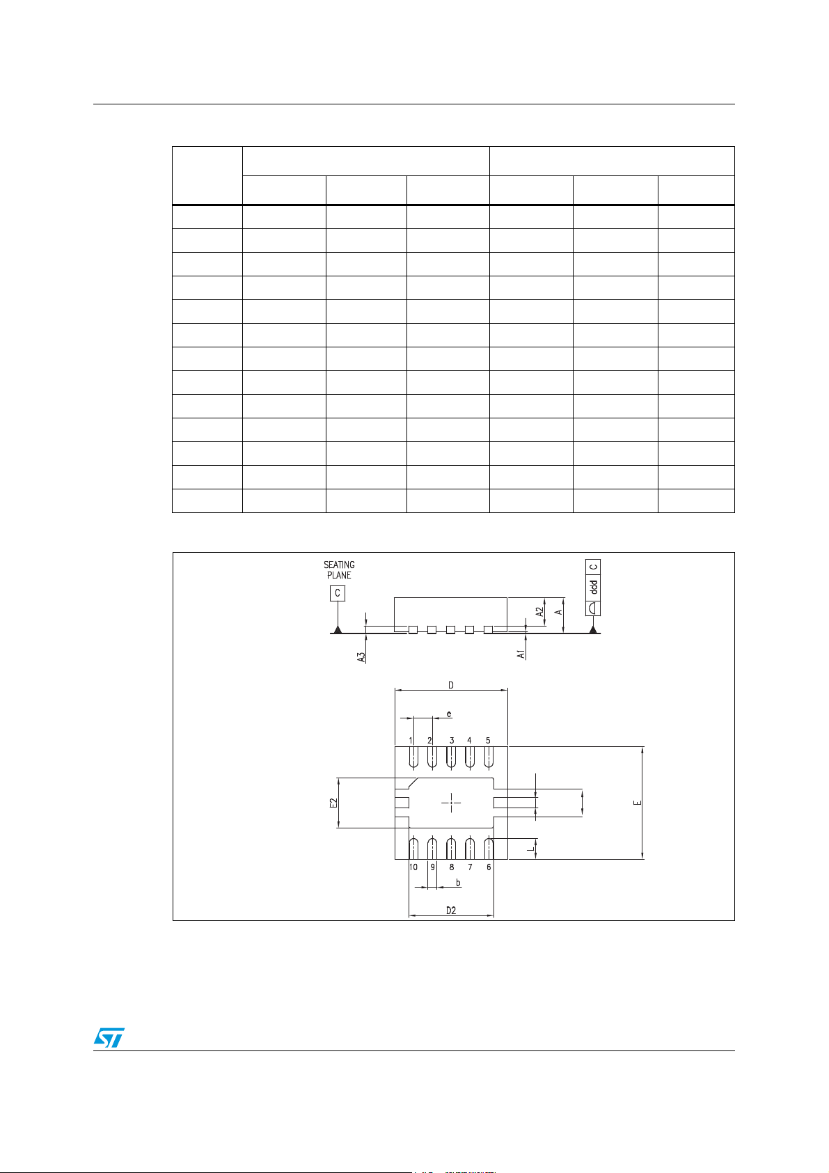
Table 10. VFDFPN10 3x3 mm mechanical data
mm mils
Dim.
Min. Typ. Max. Min. Typ. Max.
A 0.80 0.90 1.00 31.49 35.43 39.37
A1 0.02 0.05 0.787 1.968
A2 0.70 27.55
A3 0.20 7.874
b 0.18 0.23 0.30 7.086 9.055 11.81
D 3.00 118.1
D2 2.21 2.26 2.31 87.00 88.97 90.94
E 3.00 118.1
E2 1.49 1.64 1.74 58.66 64.56 68.50
e 0.50 19.68
L 0.3 0.4 0.5 11.81 15.74 19.68
M 0.75 29.52
m0.25 9.842
Figure 18. VFDFPN10 3x3 mm package drawing
M
m
Doc ID 15726 Rev 1 31/33
Page 32
Revision history L6728AH
14 Revision history
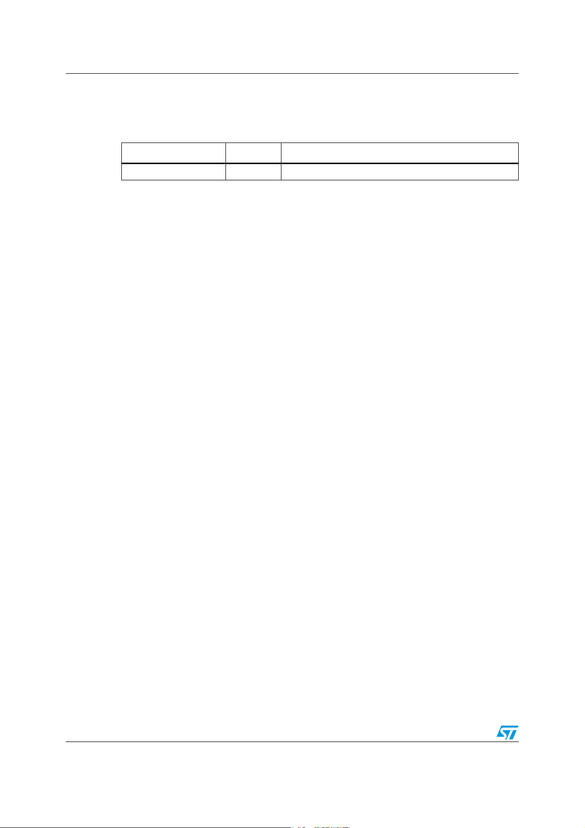
Table 11. Document revision history
Date Revision Changes
20-May-2009 1 Initial release
32/33 Doc ID 15726 Rev 1
Page 33

L6728AH
Please Read Carefully:
Information in this document is provided solely in connection with ST products. STMicroelectronics NV and its subsidiaries (“ST”) reserve the
right to make changes, corrections, modifications or improvements, to this document, and the products and services described herein at any
time, without notice.
All ST products are sold pursuant to ST’s terms and conditions of sale.
Purchasers are solely responsible for the choice, selection and use of the ST products and services described herein, and ST assumes no
liability whatsoever relating to the choice, selection or use of the ST products and services described herein.
No license, express or implied, by estoppel or otherwise, to any intellectual property rights is granted under this document. If any part of this
document refers to any third party products or services it shall not be deemed a license grant by ST for the use of such third party products
or services, or any intellectual property contained therein or considered as a warranty covering the use in any manner whatsoever of such
third party products or services or any intellectual property contained therein.
UNLESS OTHERWISE SET FORTH IN ST’S TERMS AND CONDITIONS OF SALE ST DISCLAIMS ANY EXPRESS OR IMPLIED
WARRANTY WITH RESPECT TO THE USE AND/OR SALE OF ST PRODUCTS INCLUDING WITHOUT LIMITATION IMPLIED
WARRANTIES OF MERCHANTABILITY, FITNESS FOR A PARTICULAR PURPOSE (AND THEIR EQUIVALENTS UNDER THE LAWS
OF ANY JURISDICTION), OR INFRINGEMENT OF ANY PATENT, COPYRIGHT OR OTHER INTELLECTUAL PROPERTY RIGHT.
UNLESS EXPRESSLY APPROVED IN WRITING BY AN AUTHORIZED ST REPRESENTATIVE, ST PRODUCTS ARE NOT
RECOMMENDED, AUTHORIZED OR WARRANTED FOR USE IN MILITARY, AIR CRAFT, SPACE, LIFE SAVING, OR LIFE SUSTAINING
APPLICATIONS, NOR IN PRODUCTS OR SYSTEMS WHERE FAILURE OR MALFUNCTION MAY RESULT IN PERSONAL INJURY,
DEATH, OR SEVERE PROPERTY OR ENVIRONMENTAL DAMAGE. ST PRODUCTS WHICH ARE NOT SPECIFIED AS "AUTOMOTIVE
GRADE" MAY ONLY BE USED IN AUTOMOTIVE APPLICATIONS AT USER’S OWN RISK.
Resale of ST products with provisions different from the statements and/or technical features set forth in this document shall immediately void
any warranty granted by ST for the ST product or service described herein and shall not create or extend in any manner whatsoever, any
liability of ST.
ST and the ST logo are trademarks or registered trademarks of ST in various countries.
Information in this document supersedes and replaces all information previously supplied.
The ST logo is a registered trademark of STMicroelectronics. All other names are the property of their respective owners.
© 2009 STMicroelectronics - All rights reserved
Australia - Belgium - Brazil - Canada - China - Czech Republic - Finland - France - Germany - Hong Kong - India - Israel - Italy - Japan -
STMicroelectronics group of companies
Malaysia - Malta - Morocco - Philippines - Singapore - Spain - Sweden - Switzerland - United Kingdom - United States of America
www.st.com
Doc ID 15726 Rev 1 33/33
 Loading...