

Page 1
Features
■ Selectable multimode operation: fixed
frequency or quasi-resonant
■ On-board 840 V high voltage startup
■ Advanced light load management
■ Low quiescent current (< 3 mA)
■ Adaptive UVLO
■ Line feedforward for constant power capability
vs. mains voltage
■ Pulse-by-pulse OCP, shutdown on overload
(latched or auto-restart)
■ Transformer saturation detection
■ Programmable frequency modulation for EMI
reduction
■ Latched or auto-restart OVP
■ Brownout protection
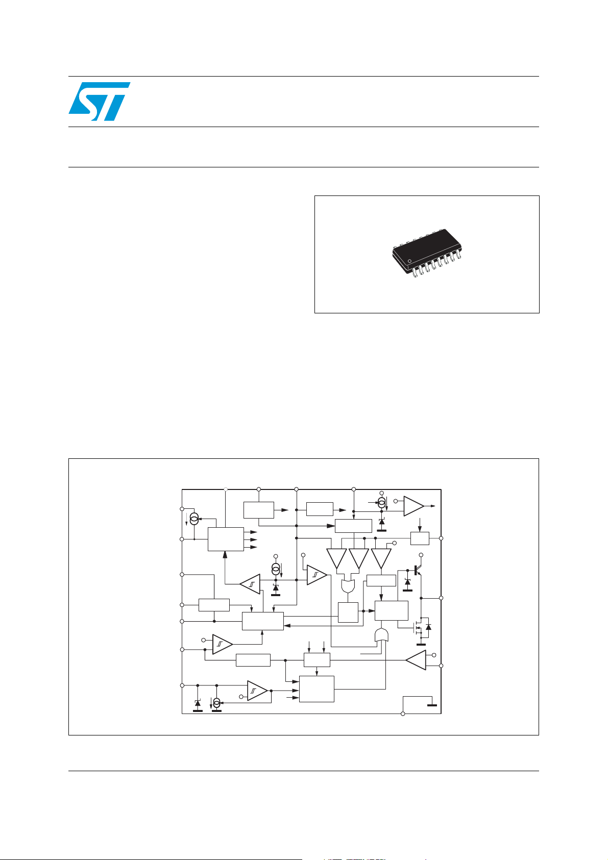
Figure 1. Block diagram
L6566BH
Multimode controller for SMPS
Datasheet — production data
SO16N
■ -600/+800 mA totem pole gate driver with
active pull-down during UVLO
■ SO16N package
Applications
■ Industrial SMPS
■ SMPS running off rectified 3-phase input line
COMP
915
TIME
OUT
LOW CLAMP
& DISABLE
Vth
V
CC
400 uA
+
-
5.7V
BURST-MODE
TIME
OVPL
OUT
OVP
LATCH
IC_LATCH
AC_ FAI L
UVLO
DISABLE
VFF
OFF2
LINE VOLTAGE
FEEDFORWARD
+-
OCPPWM
R
Q
S
OFF2
OVP
+-
V
CC
+-
Hiccup-mode
OCP logic
OCP2
DRIVER
7.7V
I
charge
6.4V
3
1.5 V
OVPL
+
Q
V
CC
14V
LEB
CS
7
4
GD
4.5V
-
+
DIS
8
FMOD
OSC
MOD E/S C
ZCD
AC_O K
VRE F
10
1
HV
I
HV
V
CC
5
6
13
12
100 mV
11
16
50 mV
3 V
VOLTAG E
REGULATOR
ADAP TIVE UVL O
OSCILL ATOR
-
+
15 µA
&
UVLO_ SHF
ZERO CURRENT
DETECTOR
OVERVOLTAGE
0.450V
0.485V
SS
14
SOFT-START
&
FAULT MNGT
Ref er e nc e
voltages
Internal supply
UVL O
-
+
MODE SELECTION
&
TURN -ON LO GIC
PROTECTION
-
+
April 2012 Doc ID 16610 Rev 2 1/51
This is information on a product in full production.
www.st.com
51
Page 2

Contents L6566BH
Contents
1 Description . . . . . . . . . . . . . . . . . . . . . . . . . . . . . . . . . . . . . . . . . . . . . . . . . 6
2 Pin settings . . . . . . . . . . . . . . . . . . . . . . . . . . . . . . . . . . . . . . . . . . . . . . . . 8
2.1 Connections . . . . . . . . . . . . . . . . . . . . . . . . . . . . . . . . . . . . . . . . . . . . . . . . 8
2.2 Pin description . . . . . . . . . . . . . . . . . . . . . . . . . . . . . . . . . . . . . . . . . . . . . . 8
3 Electrical data . . . . . . . . . . . . . . . . . . . . . . . . . . . . . . . . . . . . . . . . . . . . . 11
3.1 Maximum rating . . . . . . . . . . . . . . . . . . . . . . . . . . . . . . . . . . . . . . . . . . . . 11
3.2 Thermal data . . . . . . . . . . . . . . . . . . . . . . . . . . . . . . . . . . . . . . . . . . . . . . 11
4 Electrical characteristics . . . . . . . . . . . . . . . . . . . . . . . . . . . . . . . . . . . . 12
5 Application information . . . . . . . . . . . . . . . . . . . . . . . . . . . . . . . . . . . . . 16
5.1 High voltage startup generator . . . . . . . . . . . . . . . . . . . . . . . . . . . . . . . . . 17
5.2 Zero-current detection and triggering block; oscillator block . . . . . . . . . . 19
5.3 Burst-mode operation at no load or very light load . . . . . . . . . . . . . . . . . . 22
5.4 Adaptive UVLO . . . . . . . . . . . . . . . . . . . . . . . . . . . . . . . . . . . . . . . . . . . . . 23
5.5 PWM control block . . . . . . . . . . . . . . . . . . . . . . . . . . . . . . . . . . . . . . . . . . 24
5.6 PWM comparator, PWM latch and voltage feedforward blocks . . . . . . . . 25
5.7 Hiccup-mode OCP . . . . . . . . . . . . . . . . . . . . . . . . . . . . . . . . . . . . . . . . . . 28
5.8 Frequency modulation . . . . . . . . . . . . . . . . . . . . . . . . . . . . . . . . . . . . . . . 29
5.9 Latched disable function . . . . . . . . . . . . . . . . . . . . . . . . . . . . . . . . . . . . . . 31
5.10 Soft-start and delayed latched shutdown upon overcurrent . . . . . . . . . . . 32
5.11 OVP block . . . . . . . . . . . . . . . . . . . . . . . . . . . . . . . . . . . . . . . . . . . . . . . . . 33
5.12 Brownout protection . . . . . . . . . . . . . . . . . . . . . . . . . . . . . . . . . . . . . . . . . 36
5.13 Slope compensation . . . . . . . . . . . . . . . . . . . . . . . . . . . . . . . . . . . . . . . . . 39
5.14 Summary of L6566BH power management functions . . . . . . . . . . . . . . . 39
6 Application examples and ideas . . . . . . . . . . . . . . . . . . . . . . . . . . . . . . 43
2/51 Doc ID 16610 Rev 2
Page 3

L6566BH Contents
7 Package mechanical data . . . . . . . . . . . . . . . . . . . . . . . . . . . . . . . . . . . . 46
8 Order codes . . . . . . . . . . . . . . . . . . . . . . . . . . . . . . . . . . . . . . . . . . . . . . . 49
9 Revision history . . . . . . . . . . . . . . . . . . . . . . . . . . . . . . . . . . . . . . . . . . . 50
Doc ID 16610 Rev 2 3/51
Page 4

List of tables L6566BH
List of tables
Table 1. Pin functions . . . . . . . . . . . . . . . . . . . . . . . . . . . . . . . . . . . . . . . . . . . . . . . . . . . . . . . . . . . . . 8
Table 2. Absolute maximum ratings . . . . . . . . . . . . . . . . . . . . . . . . . . . . . . . . . . . . . . . . . . . . . . . . . 11
Table 3. Thermal data. . . . . . . . . . . . . . . . . . . . . . . . . . . . . . . . . . . . . . . . . . . . . . . . . . . . . . . . . . . . 11
Table 4. Electrical characteristics . . . . . . . . . . . . . . . . . . . . . . . . . . . . . . . . . . . . . . . . . . . . . . . . . . . 12
Table 5. L6566BH light load management features . . . . . . . . . . . . . . . . . . . . . . . . . . . . . . . . . . . . . 40
Table 6. L6566BH protection . . . . . . . . . . . . . . . . . . . . . . . . . . . . . . . . . . . . . . . . . . . . . . . . . . . . . . 40
Table 7. External circuits that determine IC behavior upon OVP and OCP . . . . . . . . . . . . . . . . . . . 44
Table 8. SO16N mechanical data . . . . . . . . . . . . . . . . . . . . . . . . . . . . . . . . . . . . . . . . . . . . . . . . . . . 46
Table 9. Order codes . . . . . . . . . . . . . . . . . . . . . . . . . . . . . . . . . . . . . . . . . . . . . . . . . . . . . . . . . . . . 49
Table 10. Document revision history . . . . . . . . . . . . . . . . . . . . . . . . . . . . . . . . . . . . . . . . . . . . . . . . . 50
4/51 Doc ID 16610 Rev 2
Page 5

L6566BH List of figures
List of figures
Figure 1. Block diagram . . . . . . . . . . . . . . . . . . . . . . . . . . . . . . . . . . . . . . . . . . . . . . . . . . . . . . . . . . . . 1
Figure 2. Typical system block diagram. . . . . . . . . . . . . . . . . . . . . . . . . . . . . . . . . . . . . . . . . . . . . . . . 7
Figure 3. Pin connection (through top view) . . . . . . . . . . . . . . . . . . . . . . . . . . . . . . . . . . . . . . . . . . . . 8
Figure 4. Multimode operation with QR option active . . . . . . . . . . . . . . . . . . . . . . . . . . . . . . . . . . . . 16
Figure 5. High voltage startup generator: internal schematic . . . . . . . . . . . . . . . . . . . . . . . . . . . . . . 17
Figure 6. Timing diagram: normal power-up and power-down sequences . . . . . . . . . . . . . . . . . . . . 18
Figure 7. Timing diagram showing short-circuit behavior (SS pin clamped at 5 V) . . . . . . . . . . . . . . 19
Figure 8. V
Figure 9. Drain ringing cycle skipping as the load is gradually reduced . . . . . . . . . . . . . . . . . . . . . . 20
Figure 10. Operation of ZCD, triggering and oscillator blocks (QR option active) . . . . . . . . . . . . . . . . 22
Figure 11. Load-dependent operating modes: timing diagrams . . . . . . . . . . . . . . . . . . . . . . . . . . . . . 23
Figure 12. Addition of an offset to the current sense lowers the burst-mode operation threshold . . . . 23
Figure 13. Adaptive UVLO block . . . . . . . . . . . . . . . . . . . . . . . . . . . . . . . . . . . . . . . . . . . . . . . . . . . . . 24
Figure 14. Possible feedback configurations that can be used with the L6566BH . . . . . . . . . . . . . . . 24
Figure 15. Externally controlled burst-mode operation by driving the COMP pin: timing diagram. . . . 25
Figure 16. Typical power capability change vs. input voltage in QR flyback converters . . . . . . . . . . . 26
Figure 17. Left: overcurrent setpoint vs. VFF voltage; right: line feedforward function block. . . . . . . . 27
Figure 18. Hiccup-mode OCP: timing diagram . . . . . . . . . . . . . . . . . . . . . . . . . . . . . . . . . . . . . . . . . . 29
Figure 19. Frequency modulation circuit . . . . . . . . . . . . . . . . . . . . . . . . . . . . . . . . . . . . . . . . . . . . . . . 30
Figure 20. Operation after latched disable activation: timing diagram . . . . . . . . . . . . . . . . . . . . . . . . . 32
Figure 21. Soft-start pin operation under different operating conditions and settings . . . . . . . . . . . . . 33
Figure 22. OVP function: internal block diagram . . . . . . . . . . . . . . . . . . . . . . . . . . . . . . . . . . . . . . . . . 34
Figure 23. OVP function: timing diagram . . . . . . . . . . . . . . . . . . . . . . . . . . . . . . . . . . . . . . . . . . . . . . . 35
Figure 24. Maximum allowed duty cycle vs. switching frequency for correct OVP detection. . . . . . . . 36
Figure 25. Brownout protection: internal block diagram and timing diagram . . . . . . . . . . . . . . . . . . . . 37
Figure 26. Voltage sensing techniques to implement brownout protection with the L6566BH . . . . . . 38
Figure 27. Slope compensation waveforms. . . . . . . . . . . . . . . . . . . . . . . . . . . . . . . . . . . . . . . . . . . . . 39
Figure 28. Typical low-cost application schematic . . . . . . . . . . . . . . . . . . . . . . . . . . . . . . . . . . . . . . . . 43
Figure 29. Typical full-feature application schematic (QR operation) . . . . . . . . . . . . . . . . . . . . . . . . . 43
Figure 30. Typical full-feature application schematic (FF operation) . . . . . . . . . . . . . . . . . . . . . . . . . . 44
Figure 31. Frequency foldback at light load (FF operation) . . . . . . . . . . . . . . . . . . . . . . . . . . . . . . . . 45
Figure 32. Latched shutdown upon mains overvoltage . . . . . . . . . . . . . . . . . . . . . . . . . . . . . . . . . . . . 45
Figure 33. SO16N package drawing . . . . . . . . . . . . . . . . . . . . . . . . . . . . . . . . . . . . . . . . . . . . . . . . . . 47
Figure 34. Recommended footprint (dimensions are in mm) . . . . . . . . . . . . . . . . . . . . . . . . . . . . . . . . 48
rating vs. temperature . . . . . . . . . . . . . . . . . . . . . . . . . . . . . . . . . . . . . . . . . . . . . . . . . 19
HV
Doc ID 16610 Rev 2 5/51
Page 6

Description L6566BH
1 Description
The L6566BH is an extremely versatile current-mode primary controller IC, specifically
designed for high-performance offline flyback converters running off rectified 3-phase input
lines. It is also suited to single-stage, single-switch, input-current-shaping converters
(single-stage PFC) for applications that must comply with EN61000-3-2 or JEITA-MITI
regulations.
Both fixed-frequency (FF) and quasi-resonant (QR) operation are supported. The user can
choose either of the two depending on application needs. The device features an externally
programmable oscillator: it defines the converter switching frequency in FF mode and the
maximum allowed switching frequency in QR mode.
When FF operation is selected, the ICs work as a standard current-mode controller with a
maximum duty cycle limited to 70% min. The oscillator frequency can be modulated to
mitigate EMI emissions.
QR operation, when selected, occurs at heavy load and is achieved through a transformer
demagnetization sensing input that triggers MOSFET turn-on. Under some conditions, ZVS
(zero-voltage switching) can be achieved. The converter’s power capability rise with the
mains voltage is compensated by line voltage feedforward. At medium and light load, as the
QR operating frequency equals the oscillator frequency, a function (valley skipping) is
activated to prevent further frequency rise and keep the operation as close to ZVS as
possible.
With either FF or QR operation, at very light load the ICs enter a controlled burst-mode
operation that, along with the built-in, non-dissipative, high-voltage startup circuit and the
low quiescent current, helps keep the consumption from the mains low and meet energy
saving recommendations.
An innovative adaptive UVLO helps minimize the issues related to the fluctuations of the
self-supply voltage due to transformer parasites.
The protection functions included in this device are: not-latched input undervoltage
(brownout), output OVP (auto-restart or latch-mode selectable), a first-level OCP with
delayed shutdown to protect the system during overload or short-circuit conditions (autorestart or latch-mode selectable), and a second-level OCP that is invoked when the
transformer saturates or there is a short-circuit of the secondary diode. A latched disable
input allows easy implementation of OTP with an external NTC, while an internal shutdown
prevents IC overheating.
Programmable soft-start, leading-edge blanking on the current sense input for greater noise
immunity, slope compensation (in FF mode only), and a shutdown function for externally
controlled burst-mode operation or remote ON/OFF control complete the features of this
device.
6/51 Doc ID 16610 Rev 2
Page 7
L6566BH Description
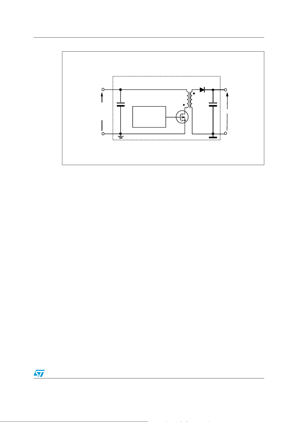
Figure 2. Typical system block diagram
FLYBAC K DC-DC CO NVERTER
Rectified
& Filtered
Mains
Voltage
L6566BH
V
outdc
Doc ID 16610 Rev 2 7/51
Page 8
Pin settings L6566BH
2 Pin settings
2.1 Connections
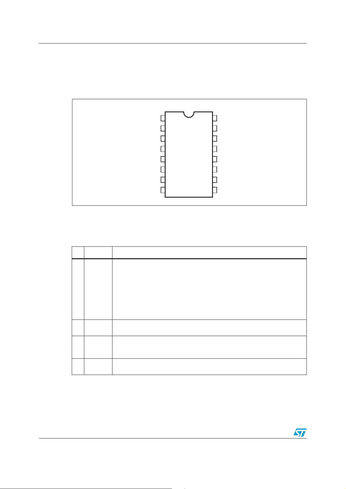
Figure 3. Pin connection (through top view)
1
16
KO_CASVH
2.2 Pin description
Table 1. Pin functions
N° Pin Function
High voltage startup. The pin, able to withstand 840 V, is to be tied directly to the
rectified mains voltage. A 1 mA internal current source charges the capacitor
connected between the Vcc pin (5) and GND pin (3) until the voltage on the Vcc pin
reaches the turn-on threshold, it is then shut down. Normally, the generator is re-
1HVS
2N.C.
enabled when the Vcc voltage falls below 5 V to ensure a low power throughput
during short-circuit. Otherwise, when a latched protection is tripped the generator is
re-enabled 0.5 V below the turn-on threshold, to keep the latch supplied; or, when
the IC is turned off by the COMP pin (9) pulled low, the generator is active just
below the UVLO threshold to allow a faster restart.
Not internally connected. Provision for clearance on the PCB to meet safety
requirements.
N. C.
GND
GD
Vcc
FMOD
DIS
2
3
4
5
6
7
8
15
14
13
12
11
10
9
VFF
SS
OSC
MODE /S C
ZCD
FERVSC
COMP
AM11479v1
Ground. Current return for both the signal part of the IC and the gate drive. All of
3GND
4GD
8/51 Doc ID 16610 Rev 2
the ground connections of the bias components should be tied to a track going to
this pin and kept separate from any pulsed current return.
Gate driver output. The totem pole output stage is able to drive Power MOSFETs
and IGBTs with a peak current capability of 800 mA source/sink.
Page 9

L6566BH Pin settings
Table 1. Pin functions (continued)
N° Pin Function
Supply voltage of both the signal part of the IC and the gate driver. The internal
high voltage generator charges an electrolytic capacitor connected between this
pin and GND (pin 3) as long as the voltage on the pin is below the turn-on threshold
5Vcc
6FMOD
7CS
of the IC, after that it is disabled and the chip is turned on. The IC is disabled as the
voltage on the pin falls below the UVLO threshold. This threshold is reduced at light
load to counteract the natural reduction of the self-supply voltage. Sometimes a
small bypass capacitor (0.1 µF typ.) to GND might be useful to obtain a clean bias
voltage for the signal part of the IC.
Frequency modulation input. When FF mode operation is selected, a capacitor
connected from this pin to GND (pin 3) is alternately charged and discharged by
internal current sources. As a result, the voltage on the pin is a symmetrical
triangular waveform with the frequency related to the capacitance value. By
connecting a resistor from this pin to pin 13 (OSC) it is possible to modulate the
current sourced by the OSC pin and then the oscillator frequency. This modulation
is to reduce the peak value of EMI emissions by means of a spread-spectrum
action. If the function is not used, the pin is left open.
Input to the PWM comparator. The current flowing in the MOSFET is sensed
through a resistor, the resulting voltage is applied to this pin and compared with an
internal reference to determine MOSFET turn-off. The pin is equipped with 150 ns
min. blanking time after the gate-drive output goes high for improved noise
immunity. A second comparison level located at 1.5 V latches the device OFF and
reduces its consumption in the case of transformer saturation or secondary diode
short-circuit. The information is latched until the voltage on the Vcc pin (5) goes
below the UVLO threshold, therefore resulting in intermittent operation. A logic
circuit improves sensitivity to temporary disturbances.
8DIS
9COMP
10 VREF
IC latched disable input. Internally, the pin connects a comparator that, when the
voltage on the pin exceeds 4.5 V, latches OFF the IC and brings its consumption to
a lower value. The latch is cleared as the voltage on the Vcc pin (5) goes below the
UVLO threshold, but the HV generator keeps the Vcc voltage high (see pin 1
description). It is then necessary to recycle the input power to restart the IC. For a
quick restart, pull pin 16 (AC_OK) below the disable threshold (see pin 16
description). Bypass the pin with a capacitor to GND (pin 3) to reduce noise pickup. Ground the pin if the function is not used.
Control input for loop regulation. The pin is driven by the phototransistor (emittergrounded) of an optocoupler to modulate its voltage by modulating the current
sunk. A capacitor placed between the pin and GND (3), as close to the IC as
possible to reduce noise pick-up, sets a pole in the output-to-control transfer
function. The dynamics of the pin are in the 2.5 to 5 V range. A voltage below an
internally defined threshold activates burst-mode operation. The voltage at the pin
is bottom-clamped at about 2 V. If the clamp is externally overridden and the
voltage is pulled below 1.4 V, the IC shuts down.
An internal generator furnishes an accurate voltage reference (5 V ± 2%) that can
be used to supply few mA to an external circuit. A small film capacitor (0.1 µF typ.),
connected between this pin and GND (3), is recommended to ensure the stability of
the generator and to prevent noise from affecting the reference. This reference is
internally monitored by a separate auxiliary reference and any failure or drift causes
the IC to latch OFF.
Doc ID 16610 Rev 2 9/51
Page 10

Pin settings L6566BH
Table 1. Pin functions (continued)
N° Pin Function
Transformer demagnetization sensing input for quasi-resonant operation and OVP
input. The pin is externally connected to the transformer’s auxiliary winding through
a resistor divider. A negative-going edge triggers MOSFET turn-on if QR mode is
11 ZCD
12 MODE/SC
13 OSC
14 SS
15 VFF
selected.
A voltage exceeding 5 V shuts the IC down and brings its consumption to a lower
value (OVP). Latch OFF or auto-restart mode is selectable externally. This function
is strobed and digitally filtered to increase noise immunity.
Operating mode selection. If the pin is connected to the VREF pin (7), quasiresonant operation is selected, the oscillator (pin 13, OSC) determines the
maximum allowed operating frequency.
Fixed-frequency operation is selected if the pin is not tied to VREF, in which case
the oscillator determines the actual operating frequency, the maximum allowed
duty cycle is set at 70% min. and the pin delivers a voltage ramp synchronized to
the oscillator when the gate-drive output is high; the voltage delivered is zero while
the gate-drive output is low. The pin is to be connected to pin CS (7) via a resistor
for slope compensation.
Oscillator pin. The pin is an accurate 1 V voltage source, and a resistor connected
from the pin to GND (pin 3) defines a current. This current is internally used to set
the oscillator frequency that defines the maximum allowed switching frequency of
the L6566BH, if working in QR mode, or the operating switching frequency if
working in FF mode.
Soft-start current source. At startup, a capacitor Css between this pin and GND
(pin 3) is charged with an internal current generator. During the ramp, the internal
reference clamp on the current sense pin (7, CS) rises linearly starting from zero to
its final value, therefore causing the duty cycle to increase progressively starting
from zero as well. During soft-start the adaptive UVLO function and all functions
monitoring the COMP pin are disabled. The soft-start capacitor is discharged
whenever the supply voltage of the IC falls below the UVLO threshold. The same
capacitor is used to delay IC shutdown (latch OFF or auto-restart mode selectable)
after detecting an overload condition (OLP).
Line voltage feedforward input. The information on the converter’s input voltage is
fed into the pin through a resistor divider and is used to change the setpoint of the
pulse-by-pulse current limitation (the higher the voltage, the lower the setpoint).
The linear dynamics of the pin ranges from 0 to 3 V. A voltage higher than 3 V
makes the IC stop switching. If feedforward is not desired, tie the pin to GND (pin 3)
directly if a latch-mode OVP is not required (see pin 11, ZCD) or through a 10 kΩ
min. resistor if a latch-mode OVP is required. Bypass the pin with a capacitor to
GND (pin 3) to reduce noise pick-up.
Brownout protection input. A voltage below 0.45 V shuts down (not latched) the IC,
lowers its consumption and clears the latch set by latched protection (DIS > 4.5 V,
SS > 6.4 V, VFF > 6.4 V). IC operation is re-enabled as the voltage exceeds 0.45 V.
16 AC_OK
10/51 Doc ID 16610 Rev 2
The comparator is provided with current hysteresis: an internal 15 µA current
generator is ON as long as the voltage on the pin is below 0.45 V and is OFF if this
value is exceeded. Bypass the pin with a capacitor to GND (pin 3) to reduce noise
pick-up. Tie to Vcc with a 220 to 680 kW resistor if the function is not used.
Page 11
L6566BH Electrical data
3 Electrical data
3.1 Maximum rating
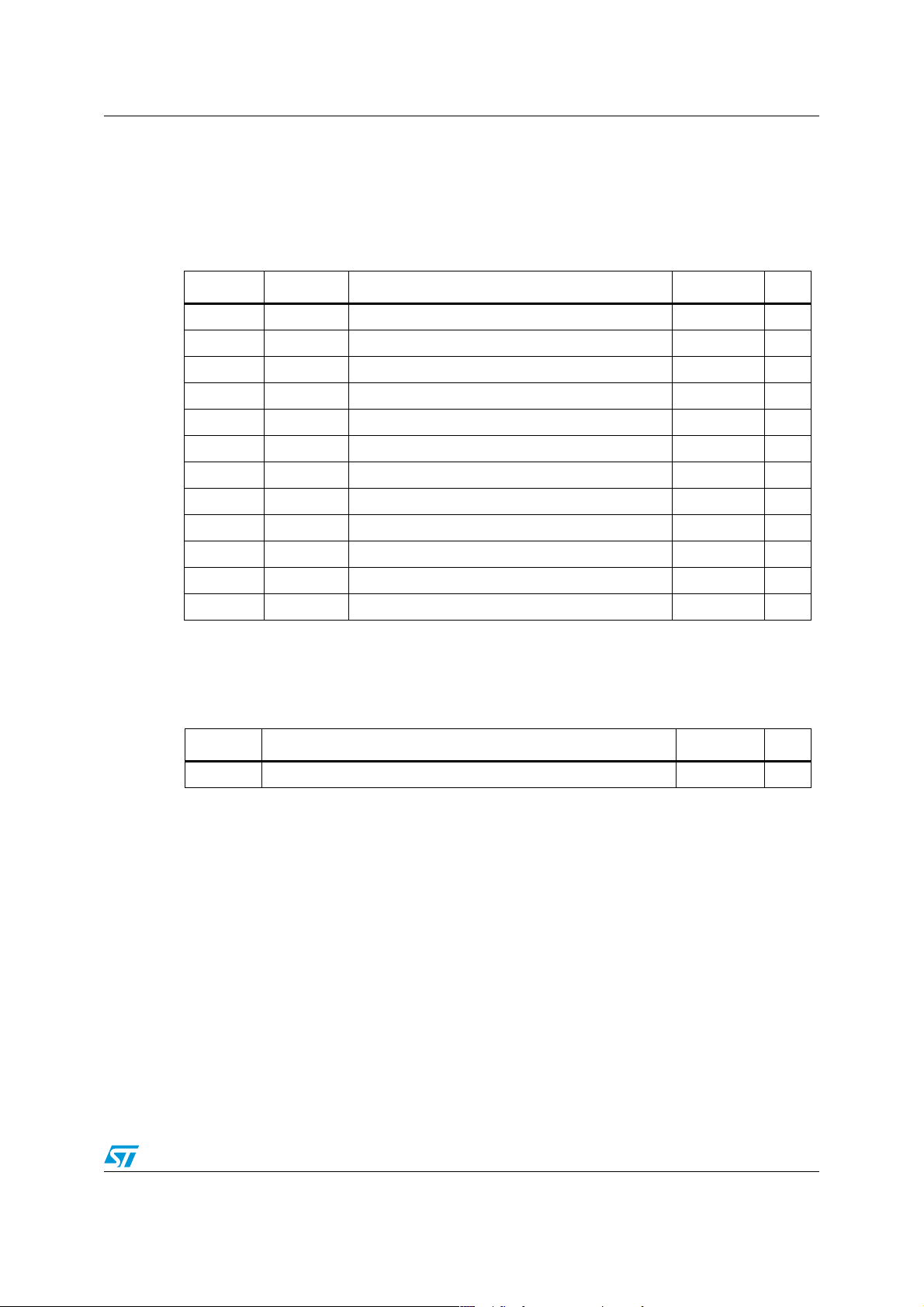
Table 2. Absolute maximum ratings
Symbol Pin Parameter Value Unit
V
HVS
I
HVS
V
CC
V
FMOD
V
max
V
max
I
ZCD
V
MODE/SC
V
OSC
P
TOT
T
STG
T
J
1 Voltage range (referred to ground) @ 25 °C -0.3 to 840 V
1 Output current Self-limited
5 IC supply voltage (Icc = 20 mA) Self-limited
6 Voltage range -0.3 to 2 V
7, 8, 10, 14 Analog inputs and outputs -0.3 to 7 V
9, 15, 16 Maximum pin voltage (Ipin ≤ 1 mA) Self-limited
11 Zero-current detector max. current ±5 mA
12 Voltage range -0.3 to 5.3 V
13 Voltage range -0.3 to 3.3 V
3.2 Thermal data
Table 3. Thermal data
Symbol Parameter Value Unit
Power dissipation @ TA = 50 °C 0.75 W
Storage temperature -55 to 150 °C
Junction operating temperature range -40 to 150 °C
R
thJA
Thermal resistance junction to ambient 120 °C/W
Doc ID 16610 Rev 2 11/51
Page 12
Electrical characteristics L6566BH
4 Electrical characteristics
(TJ = -25 to 125 °C, VCC = 12, CO = 1 nF; MODE/SC = V
, RT = 20 kΩ from OSC to GND,
REF
unless otherwise specified.)
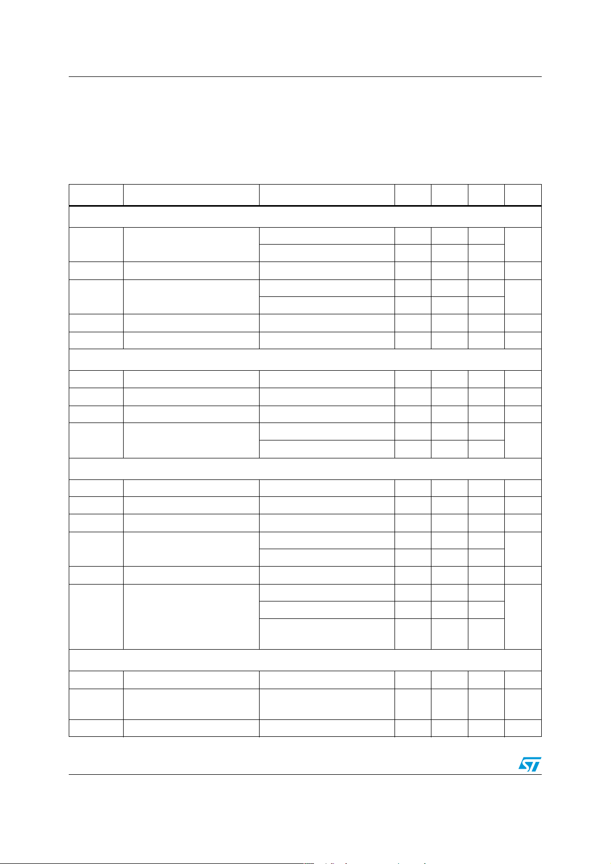
Table 4. Electrical characteristics
Symbol Parameter Test condition Min. Typ. Max. Unit
Supply voltage
Vcc Operating range after turn-on
Vcc
Vcc
Hys Hysteresis V
V
Supply current
I
start-up
I
q
Icc Operating supply current MODE/SC open 4 4.6 mA
I
qdis
V
> V
COMP
V
COMP
Turn-on threshold
On
Turn-off threshold
Off
Zener voltage Icc = 20 mA, IC disabled 23 25 27 V
Z
(1)
(1)
(1)
COMP
V
V
= V
COMP
COMP
> V
COMPL
COMPO
> V
= V
COMPL
COMPL
COMPO
10.6 23
823
13 14 15 V
9.4 10 10.6
7.2 7.6 8.0
4V
Startup current Before turn-on, Vcc = 13 V 200 250 µA
Quiescent current After turn-on, V
IC disabled
(2)
ZCD
= V
= 1 V 2.6 2.8 mA
CS
330 2500
Quiescent current
IC latched OFF 440 500
V
V
µA
High voltage startup generator
V
HV
V
HVstart
I
charge
I
HV, ON
I
HV, OFF
V
CCrestart
Breakdown voltage
Start voltage I
Vcc charge current VHV > V
ON-state current
OFF-state leakage current VHV = 400 V 40 µA
Vcc restart voltage
Reference voltage
V
V
I
REF
REF
REF
Output voltage
To t a l va r ia ti on
Short-circuit current V
(3)
I
< 100 µA @ 25 °C 840 V
HV
< 100 µA 65 80 100 V
Vcc
, Vcc > 3 V 0.55 0.85 1 mA
Hvstart
V
> V
HV
> V
V
HV
, Vcc > 3 V 1.6
Hvstart
, Vcc = 0 0.8
Hvstart
Vcc falling 4.4 5 5.6
(1)
IC latched OFF 12.5 13.5 14.5
(1)
Disabled by
V
< V
COMP
(1)
TJ = 25 °C; I
I
REF
COMPOFF
REF
= 1 to 5 mA,
= 1 mA 4.95 5 5.05 V
Vcc = 10.6 to 23 V
= 0 10 30 mA
REF
9.4 10 10.6
4.9 5.1 V
mA
V
12/51 Doc ID 16610 Rev 2
Page 13
L6566BH Electrical characteristics
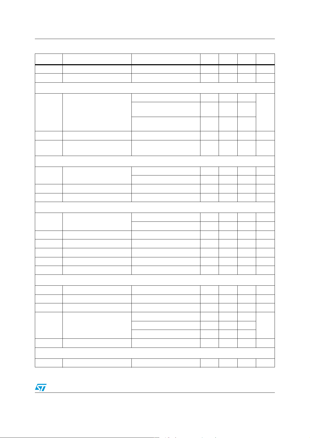
Table 4. Electrical characteristics (continued)
Symbol Parameter Test condition Min. Typ. Max. Unit
Sink capability in UVLO Vcc = 6 V; Isink = 0.5 mA 0.2 0.5 V
V
OV
Overvoltage threshold 5.3 5.7 V
Internal oscillator
Oscillation frequency
Voltage reference
Maximum duty cycle
V
D
f
sw
OSC
max
Brownout protection
Vth Threshold voltage
I
Hys
V
AC_OK_CL
Current hysteresis Vcc > 5 V, V
Clamp level
Line voltage feedforward
I
VFF
V
VFF
V
OFF
V
VFFlatch
Input bias current
Linear operation range 0 to 3 V
IC disable voltage 3 3.15 3.3 V
Latch OFF/clamp level V
Kc Control voltage gain
K
FF
Feedforward gain
Current sense comparator
(3)
(4)
Operating range 10 300
T
= 25 °C, V
J
MODE/SC = open
Vcc =12 to 23 V, V
MODE/SC = open
(4)
MODE/SC = open,
V
= 5 V
COMP
ZCD
= 0,
ZCD
= 0,
95 100 105
kHz
93 100 107
0.9711.03V
70 75 %
Voltage falling (turn-off) 0.432 0.450 0.468 V
Voltage rising (turn-on) 0.452 0.485 0.518 V
= 0.3 V 121518µA
VFF
(1)
V
V
V
V
I
VFF
ZCD
ZCD
VFF
VFF
= 100 µA 3 3.15 3.3 V
AC_OK
= 0 to 3 V, V
> V
ZCDth
> V
ZCDth
= 1 V, V
= 1 V, V
COMP
COMP
< V
ZCD
ZCDth
-0.7 -1 mA
6.4 V
= 4 V 0.4 V/V
= 4 V 0.04 V/V
-1 µA
I
CS
t
LEB
td
(H-L)
V
CSx
V
CSdis
PWM control
V
COMPHI
Input bias current VCS = 0 -1 µA
Leading edge blanking 150 250 300 ns
Delay to output 100 ns
V
Overcurrent setpoint
Hiccup-mode OCP level
Upper clamp voltage I
= V
COMP
= V
COMP
V
= V
COMP
(1)
= 0 5.7 V
COMP
COMPHI
COMPHI
COMPHI
, V
= 0 V 0.92 1 1.08
VFF
, V
= 1.5 V 0.45 0.5 0.55
VFF
, V
= 3.0 V 0 0.1
VFF
1.4 1.5 1.6 V
VV
Doc ID 16610 Rev 2 13/51
Page 14
Electrical characteristics L6566BH
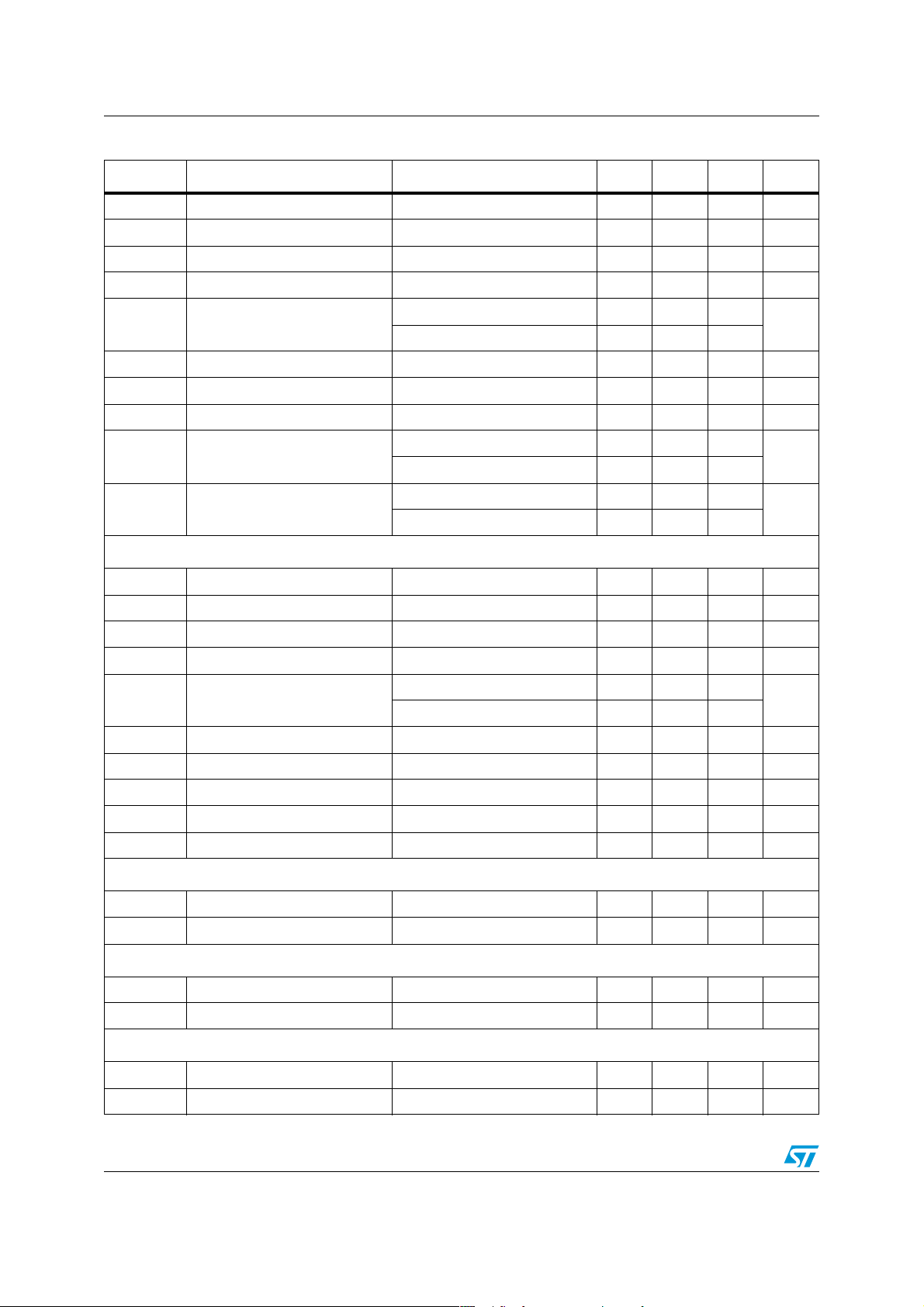
Table 4. Electrical characteristics (continued)
Symbol Parameter Test condition Min. Typ. Max. Unit
V
COMPLO
V
COMPSH
I
COMP
R
COMP
V
COMPBM
Lower clamp voltage I
Linear dynamics upper limit
Max. source current V
Dynamic resistance V
Burst-mode threshold
SOURCE
(1)
(1)
(1)
= -1 mA 2.0 V
V
= 0 V 4.855.2V
VFF
= 3.3 V 320 400 480 µA
COMP
= 2.6 to 4.8 V 25 kΩ
COMP
2.52 2.65 2.78
MODE/SC = open 2.7 2.85 3
Hys Burst-mode hysteresis 20 mV
I
CLAMPL
V
COMPOFF
V
COMPO
V
COMPL
Lower clamp capability V
= 2 V -3.5 -1.5 mA
COMP
Disable threshold Voltage falling 1.4 V
(4)
Level for lower UVLO OFF
threshold (voltage falling)
Level for higher UVLO OFF
threshold (voltage rising)
2.61 2.75 2.89
(4)
MODE/SC = open 3.02 3.15 3.28
(4)
(4)
MODE/SC = open 3.41 3.55 3.69
2.93.053.2
Zero-current detector/overvoltage protection
V
ZCDH
V
ZCDL
V
ZCDA
V
ZCDT
I
ZCD
I
ZCDsrc
I
ZCDsnk
T
BLANK1
V
ZCDth
T
BLANK2
Upper clamp voltage I
Lower clamp voltage I
Arming voltage
Triggering voltage
Internal pull-up
Source current capability V
Sink current capability V
Turn-on inhibit time After gate-drive going low 2.5 µs
OVP threshold 4.85 5 5.15 V
OVP strobe delay After gate-drive going low 2 µs
= 3 mA 5.4 5.7 6 V
ZCD
= - 3 mA -0.4 V
ZCD
(1)
Positive-going edge 85 100 115 mV
(1)
Negative-going edge 30 50 70 mV
V
COMP
V
ZCD
ZCD
ZCD
< V
COMPSH
< 2 V, V
= V
ZCDL
= V
ZCDH
COMP
= V
COMPHI
-130 -100 -70
-3 mA
3mA
-1
Latched shutdown function
V
V
V
µA
I
V
OTP
OTP
Input bias current V
Disable threshold
DIS
(1)
= 0 to V
OTP
4.32 4.5 4.68 V
Thermal shutdown
Vth Shutdown threshold 160 °C
Hys Hysteresis 50 °C
External oscillator (frequency modulation)
f
FMOD
Oscillation frequency C
= 0.1 µF 600 750 900 Hz
MOD
--- Usable frequency range 0.05 15 kHz
14/51 Doc ID 16610 Rev 2
-1 µA
Page 15
L6566BH Electrical characteristics
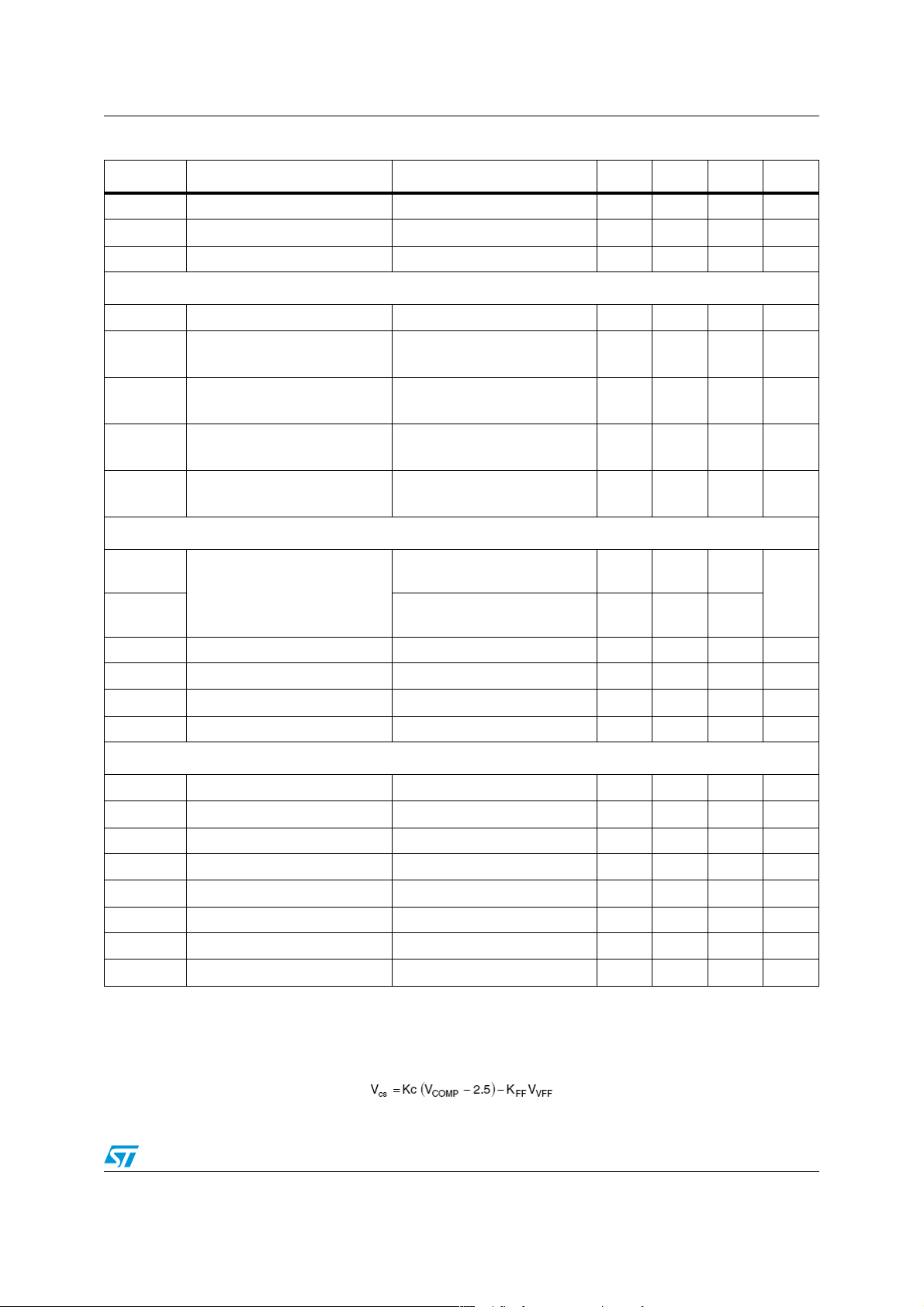
Table 4. Electrical characteristics (continued)
Symbol Parameter Test condition Min. Typ. Max. Unit
V
V
I
FMOD
pk
vy
Peak voltage
Valley voltage 0.5 V
Charge/discharge current 150 µA
Mode selection / slope compensation
(4)
1.5 V
MODE
th
SC
pk
SC
vy
Soft-start
I
SS1
I
SS2
I
SSdis
V
SSclamp
V
SSDIS
V
SSLAT
Gate driver
Threshold for QR operation 3 V
Ramp peak
(MODE/SC = open)
Ramp starting value
(MODE/SC = open)
Ramp voltage
(MODE/SC = open)
Source capability
(MODE/SC = open)
Charge current
R
pin HIGH, V
R
GD pin HIGH
GD pin LOW 0 V
V
TJ = 25 °C, VSS < 2 V,
V
TJ = 25 °C, VSS > 2 V,
V
= 3 kΩ to GND, GD
S-COMP
= 3 kΩ to GND,
S-COMP
S-COMP = VS-COMPpk
= 4 V
COMP
= V
COMP
COMP
COMPHi
= 5 V
1.7 V
0.3 V
0.8 mA
14 20 26
µA
3.556.5
Discharge current VSS > 2 V 3.556.5µA
High saturation voltage V
Disable level
Latch OFF level V
= 4 V 2 V
COMP
(1)
V
COMP
COMP
= V
= V
COMPHi
COMPHi
4.8555.15V
6.4 V
V
GDH
V
GDL
I
sourcepk
I
sinkpk
t
t
V
GDclamp
Output high voltage I
Output low voltage I
Output source peak current -0.6 A
Output sink peak current 0.8 A
Fall time 40 ns
f
Rise time 50 ns
r
Output clamp voltage I
UVLO saturation Vcc = 0 to V
1. Parameters tracking one another.
2. See
3. For the thermal behavior, refer to
4. The voltage feedforward block output is given by:
Table 6 on page 18
and
Table 7 on page 44
Figure 8
.
GDsource
GDsink
GDsource
.
= 5 mA, Vcc = 12 V 9.8 11 V
= 100 mA 0.75 V
= 5 mA; Vcc = 20 V 10 11.3 15 V
ccon, Isink = 1 mA 0.9 1.1 V
Doc ID 16610 Rev 2 15/51
Page 16
Application information L6566BH
5 Application information
The L6566BH is a versatile peak-current-mode PWM controller specific to offline flyback
converters. The device allows either fixed-frequency (FF) or quasi-resonant (QR) operation,
selectable with the MODE/SC pin (12): forcing the voltage on the pin over 3 V (e.g. by tying
it to the 5 V reference externally available at the VREF pin, 10) activates QR operation,
otherwise the device is FF-operated.
Irrespective of the operating option selected by pin 12, the device is able to work in different
modes, depending on the converter’s load conditions. If QR operation is selected (see
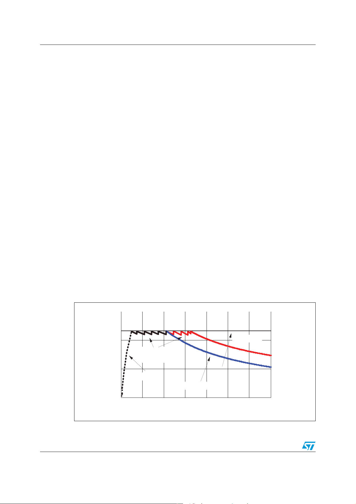
Figure 4
1. QR mode at heavy load. Quasi-resonant operation lies in synchronizing MOSFET turn-
2. Valley-skipping mode at medium/ light load. The externally programmable oscillator of
3. Burst-mode with no or very light load. When the load is extremely light or disconnected,
):
on to the transformer’s demagnetization by detecting the resulting negative-going edge
of the voltage across any winding of the transformer. Then, the system works close to
the boundary between discontinuous (DCM) and continuous conduction (CCM) of the
transformer. As a result, the switching frequency is different for different line/load
conditions (see the hyperbolic-like portion of the curves in
Figure 4
). Minimum turn-on
losses, low EMI emission and safe behavior in short-circuit are the main benefits of this
kind of operation.
the L6566BH, synchronized to MOSFET turn-on, enables the user to define the
maximum operating frequency of the converter. As the load is reduced, MOSFET turnon no longer occurs on the first valley but on the second one, the third one and so on.
In this way the switching frequency no longer increases (piecewise linear portion in
Figure 4
).
the converter enters a controlled on/off operation with constant peak current.
Decreasing the load then results in frequency reduction, which can go down even to
few hundred hertz, therefore minimizing all frequency-related losses and making it
easier to comply with energy saving regulations or recommendations. With the peak
current very low, no issue of audible noise arises.
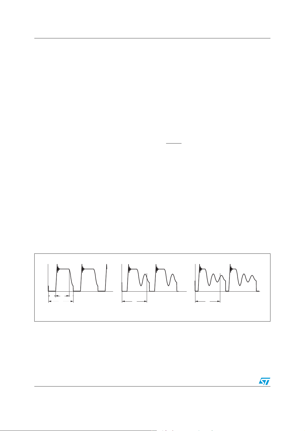
Figure 4. Multimode operation with QR option active
f
osc
Valley-skipping
f
sw
0
0
16/51 Doc ID 16610 Rev 2
mode
Burst- m ode
Quasi-resonant mode
P
in
Input voltage
Pinmax
AM11480v1
Page 17
L6566BH Application information
If FF operation is selected:
1. FF mode from heavy to light load. The system operates exactly like a standard current
mode control, at a frequency f
determined by the externally programmable oscillator:
sw
both DCM and CCM transformer operations are possible, depending on whether the
power that it processes is greater or less than:
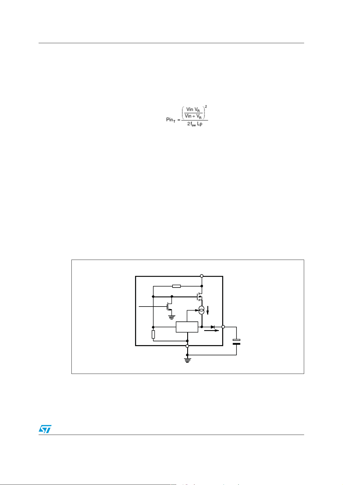
Equation 1
where Vin is the input voltage to the converter, V
regulated output voltage times the primary-to-secondary turn ratio) and Lp the
inductance of the primary winding. Pin
is the power level that marks the transition from
T
continuous to discontinuous operation mode of the transformer.
2. Burst-mode with no or very light load. This kind of operation is activated in the same
way and results in the same behavior as previously described for QR operation.
The L6566BH is specifically designed for applications with no PFC front-end; pin 6 (F
features an auxiliary oscillator that can modulate the switching frequency (when FF
operation is selected) in order to mitigate EMI emissions by a spread-spectrum action.
5.1 High voltage startup generator
Figure 5
It is made up of a high voltage N-channel FET, whose gate is biased by a 15 MΩ resistor,
with a temperature-compensated current generator connected to its source.
Figure 5. High voltage startup generator: internal schematic
shows the internal schematic of the high voltage startup generator (HV generator).
L6566BH
15 MW
the reflected voltage (i.e. the
R
HV
1
MOD
)
Vcc_OK
With reference to the timing diagram of
HV_E N
CONTROL
Figure 6
I
HV
Vcc5
I
charge
3
GND
AM11481v1
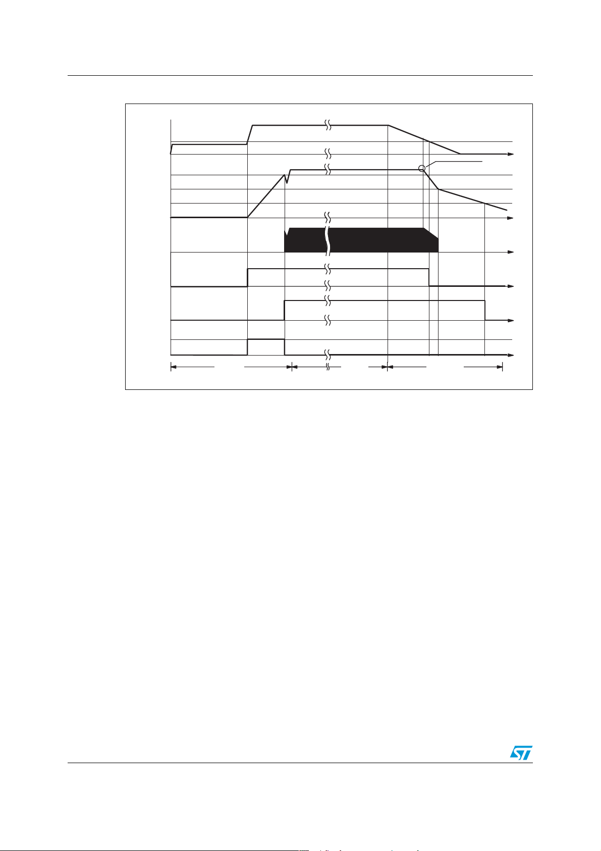
, when power is first applied to the converter
the voltage on the bulk capacitor (Vin) builds up and, at about 80 V, the HV generator is
enabled to operate (HV_EN is pulled high) so that it draws about 1 mA. This current, minus
the device consumption, charges the bypass capacitor connected from the Vcc pin (5) to
ground and makes its voltage rise almost linearly.
Doc ID 16610 Rev 2 17/51
Page 18
Application information L6566BH
Figure 6. Timing diagram: normal power-up and power-down sequences
Vin
V
HVstart
Vcc
(pin 5)
Vcc
Vcc
Vcc
restart
ON
OFF
regulation is lost here
t
GD
(pin 4)
HV_EN
cc_OK
charge
I
0.85 mA
Power-on Power-off
Normal
operation
t
t
t
t
t
AM11482v1
As the Vcc voltage reaches the turn-on threshold (14 V typ.) the device starts operating and
the HV generator is cut off by the Vcc_OK signal asserted high. The device is powered by
the energy stored in the Vcc capacitor until the self-supply circuit (typically an auxiliary
winding of the transformer and a steering diode) develops a voltage high enough to sustain
the operation. The residual consumption of this circuit is just the one on the 15 MΩ resistor
(≈ 10 mW at 400 Vdc), typically 50-70 times lower, under the same conditions, as compared
to a standard startup circuit made with external dropping resistors.
At converter power-down the system loses regulation as soon as the input voltage is so low
that either peak current or maximum duty cycle limitation is tripped. Vcc then drops and
stops IC activity as it falls below the UVLO threshold (10 V typ.). The V
asserted as the Vcc voltage goes below a threshold V
generator can now restart. However, if Vin < Vin
, as illustrated in
start
located at about 5 V. The HV
CCrest
_OK signal is de-
CC
Figure 6
, HV_EN is deasserted too and the HV generator is disabled. This prevents converter restart attempts and
ensures monotonic output voltage decay at power-down in systems where brownout
protection (see the relevant section) is not used.
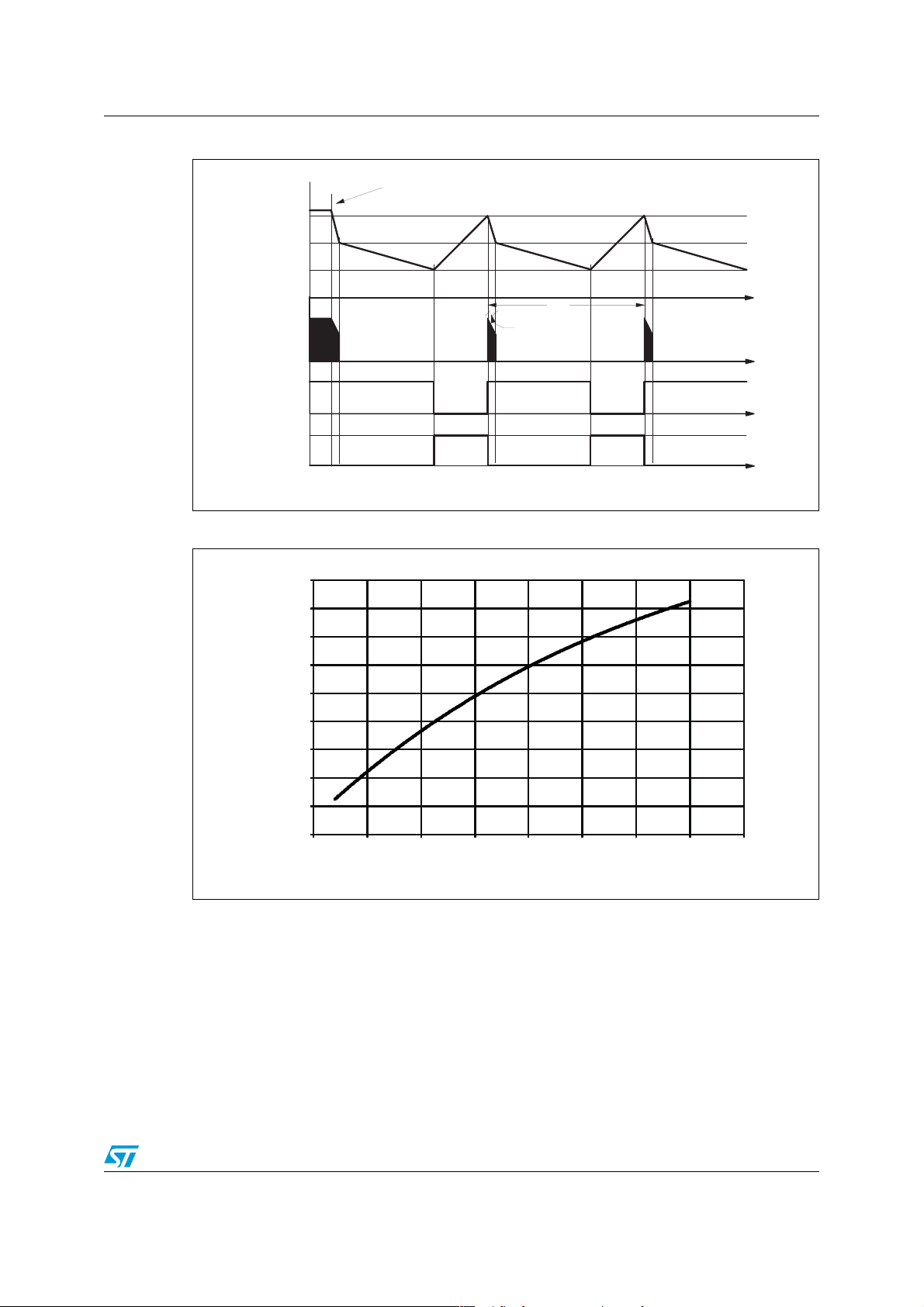
The low restart threshold V
ensures that, during short-circuits, the restart attempts of
CCrest
the device have a very low repetition rate, as shown in the timing diagram of
that the converter works safely with extremely low power throughput.
18/51 Doc ID 16610 Rev 2
Figure 7
, and
Page 19
L6566BH Application information
Figure 7. Timing diagram showing short-circuit behavior (SS pin clamped at 5 V)
Vcc
(pin 5)
Vc c
Vcc
Vcc
GD
(pin 4)
Vcc_OK
charge
I
0.85 mA
Figure 8. V
C)
°
Short circuit occurs here
ON
OFF
restart
rating vs. temperature
HV
1.080
1.060
1.040
1.020
1.000
< 0.03T
T
rep
rep
t
t
t
AM11483v1
0.980
0.960
VHV (normalized @ 25
0.940
0.920
0.900
-50 -25 0 25 50 75 100 125 150
Tj ( C)
AM11484v1
5.2 Zero-current detection and triggering block; oscillator block
The zero-current detection (ZCD) and triggering blocks switch on the external MOSFET if a
negative-going edge falling below 50 mV is applied to the input (pin 11, ZCD). To do so, the
triggering block must be previously armed by a positive-going edge exceeding 100 mV.
This feature is typically used to detect transformer demagnetization for QR operation, where
the signal for the ZCD input is obtained from the transformer’s auxiliary winding used also to
supply the L6566BH. The triggering block is blanked for T
Doc ID 16610 Rev 2 19/51
= 2.5 µs after MOSFET
BLANK
Page 20
Application information L6566BH
V
turn-off to prevent any negative-going edge that follows leakage inductance
demagnetization from triggering the ZCD circuit erroneously.
The voltage at the pin is both top and bottom limited by a double clamp, as illustrated in the
internal diagram of the ZCD block of
Figure 8
. The upper clamp is typically located at 5.7 V,
while the lower clamp is located at -0.4 V. The interface between the pin and the auxiliary
winding is a resistor divider. Its resistance ratio is properly chosen (see
block
) and the individual resistance values (RZ1, RZ2) are such that the current sourced and
Section 5.11: OVP
sunk by the pin is within the rated capability of the internal clamps (± 3 mA).
At converter power-up, when no signal is coming from the ZCD pin, the oscillator starts up
the system. The oscillator is programmed externally by means of a resistor (R
from the OSC pin (13) to ground. With good approximation the oscillation frequency f
) connected
T
osc
is:
Equation 2
3
102f⋅
≈
osc
R
T
(with f
in kHz and RT in kΩ). As the device is turned on, the oscillator starts immediately;
osc
at the end of the first oscillator cycle, the voltage on the ZCD pin being zero, the MOSFET is
turned on, therefore starting the first switching cycle right at the beginning of the second
oscillator cycle. At any switching cycle, the MOSFET is turned off as the voltage on the
current sense pin (CS, 7) hits an internal reference set by the line feedforward block, and the
transformer starts demagnetization. If this completes (so a negative-going edge appears on
the ZCD pin) after a time exceeding one oscillation period T
osc
= 1/f
turn-on, the MOSFET is turned on again – with some delay to ensure minimum voltage at
turn-on – and the oscillator ramp is reset. If, on the other hand, the negative-going edge
appears before T
T
turns on the MOSFET and synchronizes the oscillator. In this way one or more drain
osc
ringing cycles are skipped (“valley-skipping mode”,
prevented from exceeding f
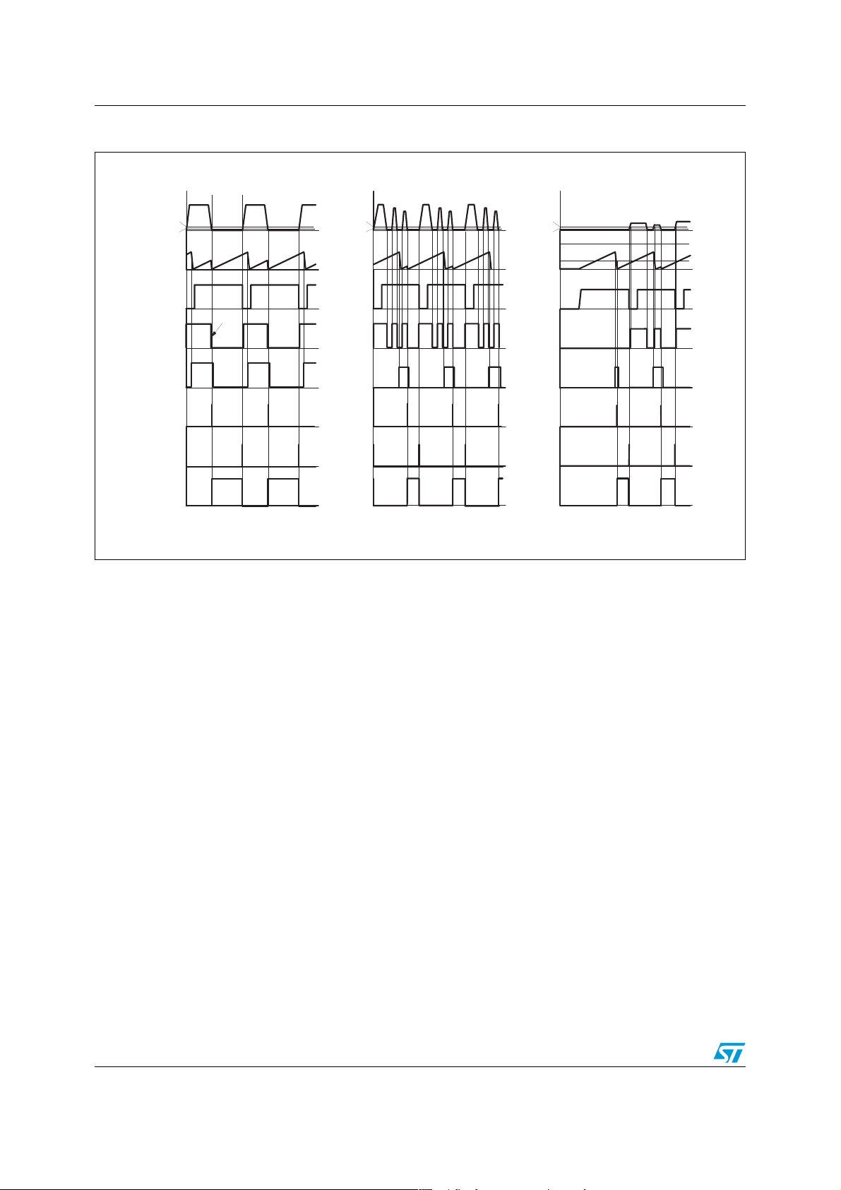
Figure 9. Drain ringing cycle skipping as the load is gradually reduced
DS
T
T
FW
osc
T
V
Pin = Pin'
(limit cond ition)
T
ON
has elapsed, it is ignored and only the first negative-going edge after
osc
Figure 9
.
osc
V
DS
t
T
osc
in''
< P
in'
Pin= P
) and the switching frequency is
V
DS
t
T
osc
from the previous
osc
in'''
< P
in''
Pin= P
t
AM11485v1
Note: When the system operates in valley skipping-mode, uneven switching cycles may be
observed under some line/load conditions, due to the fact that the OFF-time of the MOSFET
is allowed to change with discrete steps of one ringing cycle, while the OFF-time needed for
cycle-by-cycle energy balance may fall in between. Therefore, one or more longer switching
cycles is compensated by one or more shorter cycles and vice versa. However, this
mechanism is absolutely normal and there is no appreciable effect on the performance of
the converter or on its output voltage.
20/51 Doc ID 16610 Rev 2
Page 21

L6566BH Application information
If the MOSFET is enabled to turn on but the amplitude of the signal on the ZCD pin is
smaller than the arming threshold for some reason (e.g. a heavy damping of drain
oscillations, like in some single-stage PFC topologies, or when a turn-off snubber is used),
MOSFET turn-on cannot be triggered. This is identical to what happens at startup: at the
end of the next oscillator cycle the MOSFET is turned on, and a new switching cycle takes
place after skipping no more than one oscillator cycle.
The operation described so far does not consider the blanking time T
turn-off, and actually T
does not come into play as long as the following condition is
BLANK
after MOSFET
BLANK
met:
Equation 3
T
BLANK
1D −≤
T
osc
where D is the MOSFET duty cycle. If this condition is not met, there are no substantial
changes: the time during which MOSFET turn-on is inhibited is extended beyond T
fraction of T
than the programmed value f
than expected. However this is quite unusual: setting f
be observed at duty cycles higher than 60%. See
implications of T
. As a consequence, the maximum switching frequency is a little lower
BLANK
BLANK
.
and valley-skipping mode may take place slightly earlier
osc
= 150 kHz, the phenomenon can
osc
Section 5.11: OVP block
for further
osc
by a
If the voltage on the COMP pin (9) saturates high, which reveals an open control loop, an
internal pull-up keeps the ZCD pin close to 2 V during MOSFET OFF-time to prevent noise
from false triggering the detection block. When this pull-up is active, the ZCD pin may not be
able to go below the triggering threshold, which would stop the converter. To allow autorestart operation, however ensuring minimum operating frequency in these conditions, the
oscillator frequency that retriggers MOSFET turn-on is that of the external oscillator divided
by 128. Additionally, to prevent malfunction at converter startup, the pull-up is disabled
during the initial soft-start (see the relevant section). However, to ensure a correct startup, at
the end of the soft-start phase the output voltage of the converter must meet the condition:
Equation 4
Vout >
Ns
Naux
IR
ZCD1Z
where Ns is the turn number of the secondary winding, Naux the turn number of the
auxiliary winding and I
the maximum pull-up current (130 µA).
ZCD
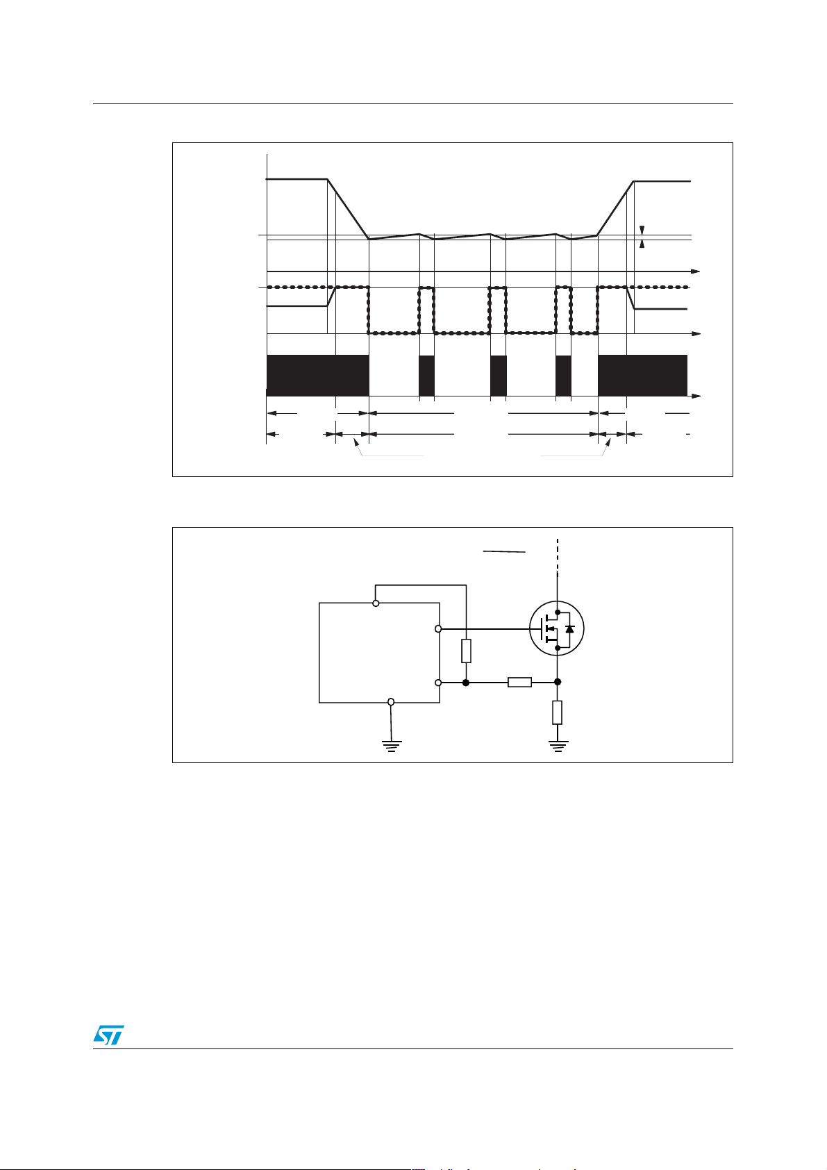
The operation described so far under different operating conditions for the converter is
illustrated in the timing diagrams of
Figure 10
.
If the FF option is selected the operation is exactly equal to that of a standard current-mode
PWM controller. It works at a frequency fsw = fosc; both DCM and CCM transformer
operations are possible, depending on the operating conditions (input voltage and output
load) and on the design of the power stage. The MOSFET is turned on at the beginning of
each oscillator cycle and is turned off as the voltage on the current sense pin reaches an
internal reference set by the line feedforward block. The maximum duty cycle is limited to
70% minimum. The signal on the ZCD pin in this case is used only for detecting feedback
loop failures (see
Section 5.11: OVP block
Doc ID 16610 Rev 2 21/51
).
Page 22
Application information L6566BH
ZCD
(pin 11)
100 mV
50 mV
Oscillato r
ramp
ZCD
blanking
tim e
Arm / Tr i g g e r
ON-e nable
PWM latch
Set
PWM latch
Reset
GD
(pin 4)
armed trigger
a) full load
ZCD
(pin 11)
100 mV
50 mV
Oscillato r
ramp
ZCD
blanking
time
Arm /Tri g g e r
ON-e nable
PWM latch
Set
PWM latch
Reset
GD
(pin 4)
b) light load
ZCD
(pin 11)
100 mV
50 mV
Oscillato r
ramp
ZCD
blanking
time
Arm/Trigger
ON- enable
PWM latch
Set
PWM latch
Reset
GD
(pin 4)
c) start-up
Figure 10. Operation of ZCD, triggering and oscillator blocks (QR option active)
AM11486v1
5.3 Burst-mode operation at no load or very light load
When the voltage at the COMP pin (9) falls 20 mV below a threshold fixed internally at a
value, V
COMPBM
the MOSFET kept in OFF-state and its consumption reduced to a lower value to minimize
V
capacitor discharge.
CC
The control voltage now increases as a result of the feedback reaction to the energy delivery
stop (the output voltage is slowly decaying), the threshold is exceeded and the device
restarts switching again. In this way the converter works in burst-mode with a nearly
constant peak current defined by the internal disable level. A load decrease then causes a
frequency reduction, which can go down even to few hundred hertz, therefore minimizing all
frequency-related losses and making it easier to comply with energy saving regulations.
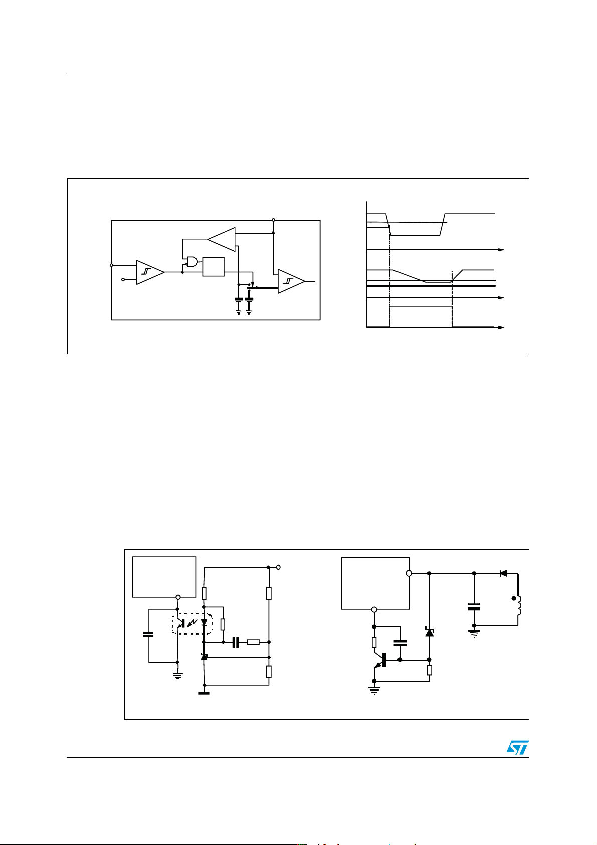
This kind of operation, shown in the timing diagrams of
previously described, is noise-free since the peak current is low.
If it is necessary to decrease the intervention threshold of the burst-mode operation, this can
be done by adding a small DC offset on the current sense pin as shown in
Note: The offset reduces the available dynamics of the current signal; thereby, the value of the
sense resistor must be determined taking this offset into account.
, depending on the selected operating mode, the L6566BH is disabled with
Figure 11
along with the others
Figure 12
.
22/51 Doc ID 16610 Rev 2
Page 23
L6566BH Application information
Figure 11. Load-dependent operating modes: timing diagrams
COMP
(pin 9)
20 mV
V
COMPBM
hyster.
f
osc
sw
f
MODE/SC=Ope n
MODE/SC=V REF
GD
(pin 4)
MODE/SC=Ope n
MODE/SC=VREF
FF Mode Burst-mode FF Mode
QR Mode
Burst-mode
Valley-skipping Mode
QR Mode
Figure 12. Addition of an offset to the current sense lowers the burst-mode
operation threshold
R
R + Rc
Rc
R
Vref
10
L6566BH
3
Vcso= Vref
4
7
t
t
t
AM11487v1
5.4 Adaptive UVLO
A major problem when optimizing a converter for minimum no-load consumption is that the
voltage generated by the auxiliary winding under these conditions falls considerably as
compared even to a few mA load. This very often causes the supply voltage Vcc of the
control IC to drop and go below the UVLO threshold so that the operation becomes
intermittent, which is undesired. Furthermore, this must be traded off against the need to
generate a voltage not exceeding the maximum allowed by the control IC at full load.
To help the user overcome this problem, the device, besides reducing its own consumption
during burst-mode operation, also features a proprietary adaptive UVLO function. It consists
of shifting the UVLO threshold downwards at light load, namely when the voltage at the
COMP pin falls below a threshold V
Rs
AM11488v1
internally fixed, so as to have more headroom. To
COMPO
Doc ID 16610 Rev 2 23/51
Page 24
Application information L6566BH
prevent any malfunction during transients from minimum to maximum load the normal
(higher) UVLO threshold is re-established when the voltage at the COMP pin exceeds
V
and Vcc has exceeded the normal UVLO threshold (see
COMPL
Figure 13
). The normal
UVLO threshold ensures that at full load the MOSFET is driven with a proper gate-to-source
voltage.
COMP
9
V
V
COMPL
COMPO
VCOMP
Vcc
Vcc
SW
(*)
OFF2
5
UVLO
+
-
L6566BH
+
-
-
+
R
S Q
Vcc
OFF1
(pin 9)
V
COMPL
V
COMPO
Vcc
(pin 5)
Vcc
Vcc
OFF1
OFF2
t
Q
t
Figure 13. Adaptive UVLO block
(*) Vcc
< Vcc
is selec ted when Q is hig h
OFF2
OFF1
5.5 PWM control block
The device is specific to secondary feedback. Typically, there is a TL431 on the secondary
side and an optocoupler that transfers output voltage information to the PWM control on the
primary side, crossing the isolation barrier. The PWM control input (pin 9, COMP) is driven
directly by the phototransistor’s collector (the emitter is grounded to GND) to modulate the
duty cycle (
In applications where a tight output regulation is not required, it is possible to use a primarysensing feedback technique. In this approach the voltage generated by the self-supply
winding is sensed and regulated. This solution, shown in
is cheaper because no optocoupler or secondary reference is needed, but output voltage
regulation, especially as a result of load changes, is quite poor.
Figure 14. Possible feedback configurations that can be used with the L6566BH
Figure 14
L6566BH
, left-hand side circuit).
9
COMP
Vout
L6566BH
9
COMP
Figure 14
5 Vcc
t
AM11489v1
, right-hand side circuit,
Cs
aux
N
TL431
Secondary feedback Primary f eedback
24/51 Doc ID 16610 Rev 2
AM11490v1
Page 25
L6566BH Application information
Ideally, the voltage generated by the self-supply winding and the output voltage should be
given by the relation between the Naux/Ns turn ratio only. Actually, numerous non-idealities,
mainly transformer parasites, cause the actual ratio to deviate from the ideal one. Line
regulation is quite good, in the range of ± 2%, whereas load regulation is about ± 5% and
output voltage tolerance is in the range of ± 10%.
The dynamics of the pin are in the 2.5 to 5 V range. The voltage at the pin is clamped
downwards at about 2 V. If the clamp is externally overridden and the voltage on the pin is
pulled below 1.4 V, the L6566BH shuts down. This condition is latched as long as the device
is supplied. While the device is disabled, however, no energy is coming from the self-supply
circuit, therefore the voltage on the Vcc capacitor decays and crosses the UVLO threshold
after some time, which clears the latch and lets the HV generator restart. This function is
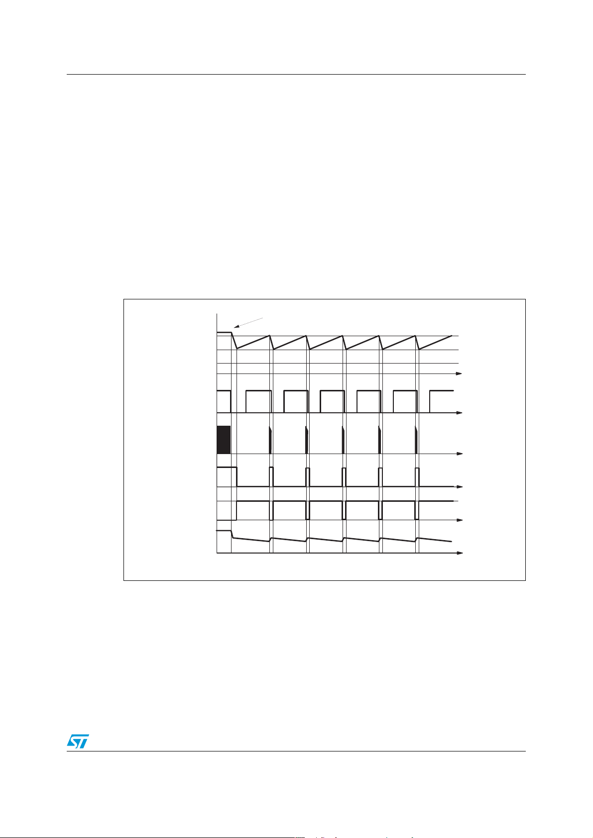
intended for an externally controlled burst-mode operation at light load with a reduced
output voltage, a technique typically used in multi-output SMPS, such as those for TVs or
monitors (see the timing diagram
Figure 15
).
Figure 15. Externally controlled burst-mode operation by driving the COMP pin:
timing diagram
Vcc
(pin 5)
Vcc
Vcc
restart
Vcc
COMP
(pin 9)
GD
(pin 4)
Vcc _OK
charge
I
0.85 mA
Vout
Standby is commanded her e
ON
OFF
t
t
t
t
t
t
AM11491v1
5.6 PWM comparator, PWM latch and voltage feedforward blocks
The PWM comparator senses the voltage across the current sense resistor Rs and, by
comparing it to the programming signal delivered by the feedforward block, determines the
exact time when the external MOSFET is to be switched off. Its output resets the PWM
latch, previously set by the oscillator or the ZCD triggering block, which asserts the gate
driver output low. The use of PWM latch avoids spurious switching of the MOSFET that may
result from the noise generated (“double-pulse suppression”).
Doc ID 16610 Rev 2 25/51
Page 26
Application information L6566BH
Cycle-by-cycle current limitation is realized with a second comparator (OCP comparator)
that senses the voltage across the current sense resistor Rs as well and compares this
voltage to a reference value V
the circuit schematic in
Figure 17
feedforward block and sent to the PWM comparator exceeds V
to reset first the PWM latch instead of the PWM comparator. The value of V
. Its output is OR-ed with that of the PWM comparator (see
CSX
). In this way, if the programming signal delivered by the
, it is the OCP comparator
CSX
csx, thereby,
determines the overcurrent setpoint along with the sense resistor Rs.
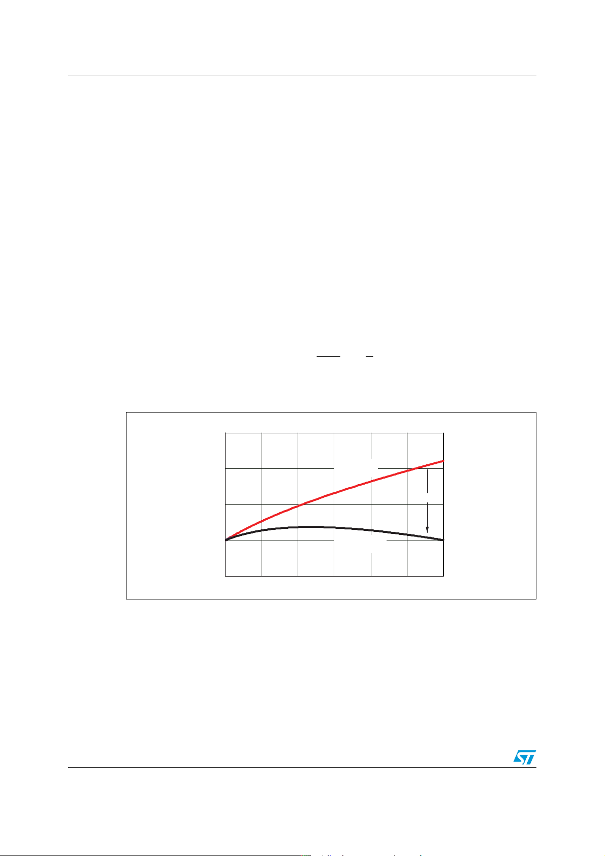
The power that QR flyback converters with a fixed overcurrent setpoint (like fixed-frequency
systems) are able to deliver changes considerably with the input voltage. With wide-range
mains, at maximum line it can be more than twice the value at minimum line, as shown by
the upper curve in the diagram of
Figure 16
. The device has the line feedforward function
available to solve this issue.
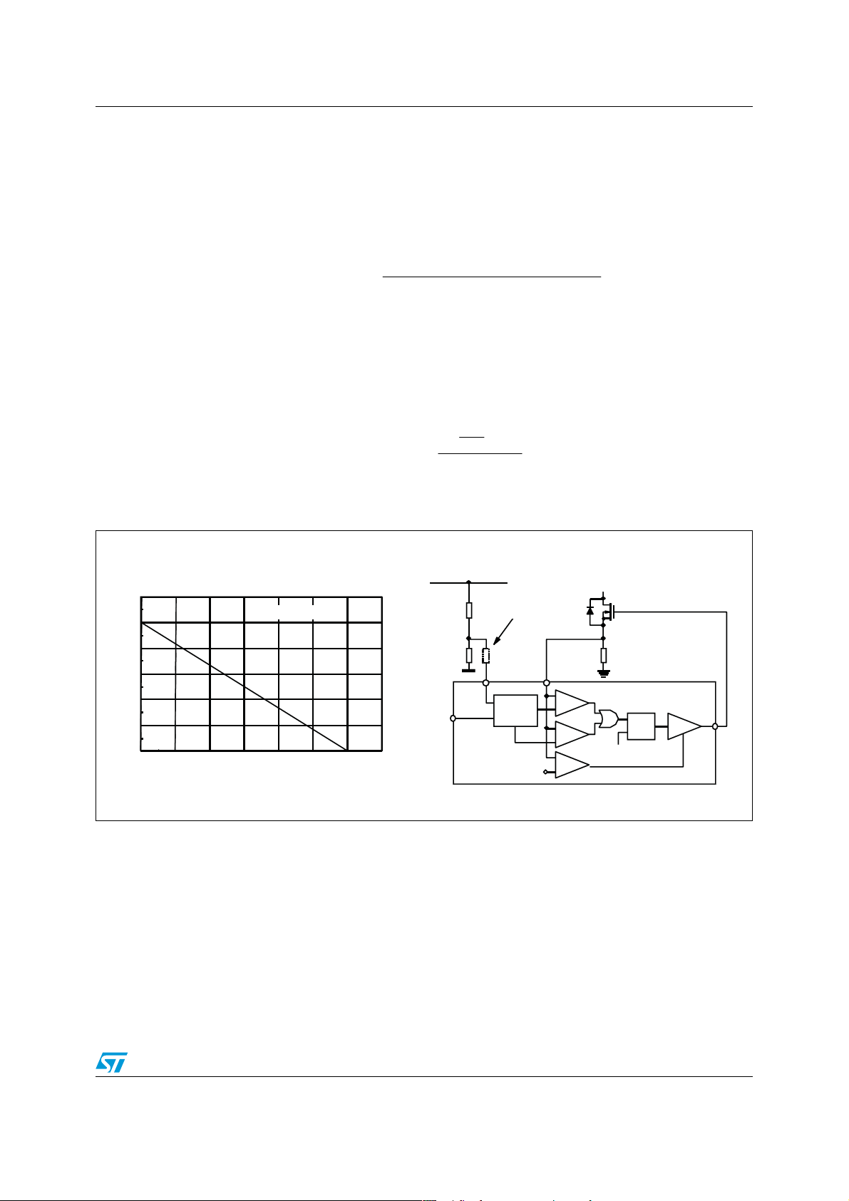
It acts on the overcurrent setpoint V
, so that it is a function of the converter’s input voltage
CSX
Vin sensed through a dedicated pin (15, VFF): the higher the input voltage, the lower the
setpoint. This is illustrated in the diagram on the left-hand side of
relationship between the voltage on the pin VFF and V
(with the error amplifier saturated
CSX
Figure 17
: it shows the
high in the attempt to obtain output voltage regulation):
Equation 5
csx
V
VFF
1V
3
k
Vin
1
−=−=
3
Figure 16. Typical power capability change vs. input voltage in QR flyback
converters
2.5
2
1.5
1
system not
compensated
system optimally
compensated
k = 0
k = k
k
opt
0.5
11.522.5 33.5 4
AM11492v1
Note: If the voltage on the pin exceeds 3 V, switching ceases but the soft-start capacitor is not
discharged. The schematic in Figure 17 shows also how the function is included in the
control loop.
With a proper selection of the external divider R1-R2, i.e. of the ratio k = R2 / (R1+R2), it is
possible to achieve the optimum compensation described by the lower curve in the diagram
of
Figure 16
The optimum value of k, k
.
, which minimizes the power capability variation over the input
opt
voltage range, is the one that provides equal power capability at the extremes of the range.
The exact calculation is complex, and non-idealities shift the real-world optimum value from
26/51 Doc ID 16610 Rev 2
Page 27
L6566BH Application information
the theoretical one. It is therefore more practical to provide a first cut value, simple to
calculate, and then to fine tune experimentally.
Assuming that the system operates exactly at the boundary between DCM and CCM, and
neglecting propagation delays, the following expression for k
can be found:
opt
Equation 6
V
opt
3k
⋅=
R
()
VVVVV
⋅++⋅
Rmaxinmininmaxinminin
Experience shows that this value is typically lower than the real one. Once the maximum
peak primary current, I
PKpmax
, occurring at minimum input voltage Vin
has been found,
min
the value of Rs can be determined from (5):
Equation 7
k
opt
1Rs−
=
V
minin
3
I
maxPKp
Figure 17. Left: overcurrent setpoint vs. VFF voltage; right: line feedforward function block
cs x
V
[V]
1.2
V
= Upper clamp
1
0.8
0.6
0.4
0.2
0
0 0.5 1 1.5 2 2 .5 33.5
COMP
VFF
V
[V]
The converter is then tested on the bench to find the output power level Pout
regulation is lost (because overcurrent is being tripped) both at Vin = Vin
Vin = Vin
If Pout
increase; if Pout
@ Vin
lim
max
.
> Pout
max
lim
@ Vin
lim
max
@ Vin
< Pout
Rectified Line Voltage
R1
R2
COMP
9
L6566BH
the system is still undercompensated and k needs to
min
@ Vin
lim
min
Optional for
OVP setti ngs
Rs
VFF CS
15
VOLTAGE
FEED
FORWA RD
Vcsx
1.5 V
7
+
PWM
-
+
OCP
-
+
Hic cup
-
Clock/ZCD
R
S
min
Q
DISABLE
lim
and
DRIVER
AM11493v1
where
the system is overcompensated and k
4
needs to decrease. This goes on until the difference between the two values is acceptably
low. Once the true k
is found in this way, it is possible that Pout
opt
can turn out slightly
lim
different from the target; to correct this, the sense resistor Rs needs to be adjusted and the
above tuning process is repeated with the new Rs value. Typically, a satisfactory setting is
achieved in no more than a couple of iterations.
GD
Doc ID 16610 Rev 2 27/51
Page 28

Application information L6566BH
In applications where this function is not wanted, e.g. because of a narrow input voltage
range, the VFF pin can be simply grounded, directly or through a resistor, depending on
whether the user wants the OVP function to be auto-restart or latched mode (see
“
Section 5.11: OVP block
”). The overcurrent setpoint is then fixed at the maximum value of 1
V. If a lower setpoint is desired to reduce the power dissipation on Rs, the pin can be also
biased at a fixed voltage using a divider from VREF (pin 10).
If the FF option is selected the line feedforward function can be still used to compensate for
the total propagation delay Td of the current sense chain (internal propagation delay td
(H-L)
plus the turn-off delay of the external MOSFET), which in standard current mode PWM
controllers is done by adding an offset on the current sense pin proportional to the input
voltage. In that case the divider ratio k, which is much smaller as compared to that used with
the QR option selected, can be calculated with the following equation:
Equation 8
opt
LpRs
Td
3k
=
where Lp is the inductance of the primary winding. In case a constant maximum power
capability vs. the input voltage is not required, the VFF pin can be grounded, directly or
through a resistor (see
Section 5.11: OVP block
), therefore fixing the overcurrent setpoint at
1 V, or biased at a fixed voltage through a divider from VREF to obtain a lower setpoint.
It is possible to bypass the pin to ground with a small film capacitor (e.g. 1-10 nF) to ensure
a clean operation of the IC even in a noisy environment.
The pin is internally forced to ground during UVLO, after activating any latched protection
and when the COMP pin is pulled below its low clamp voltage (see
control block
).
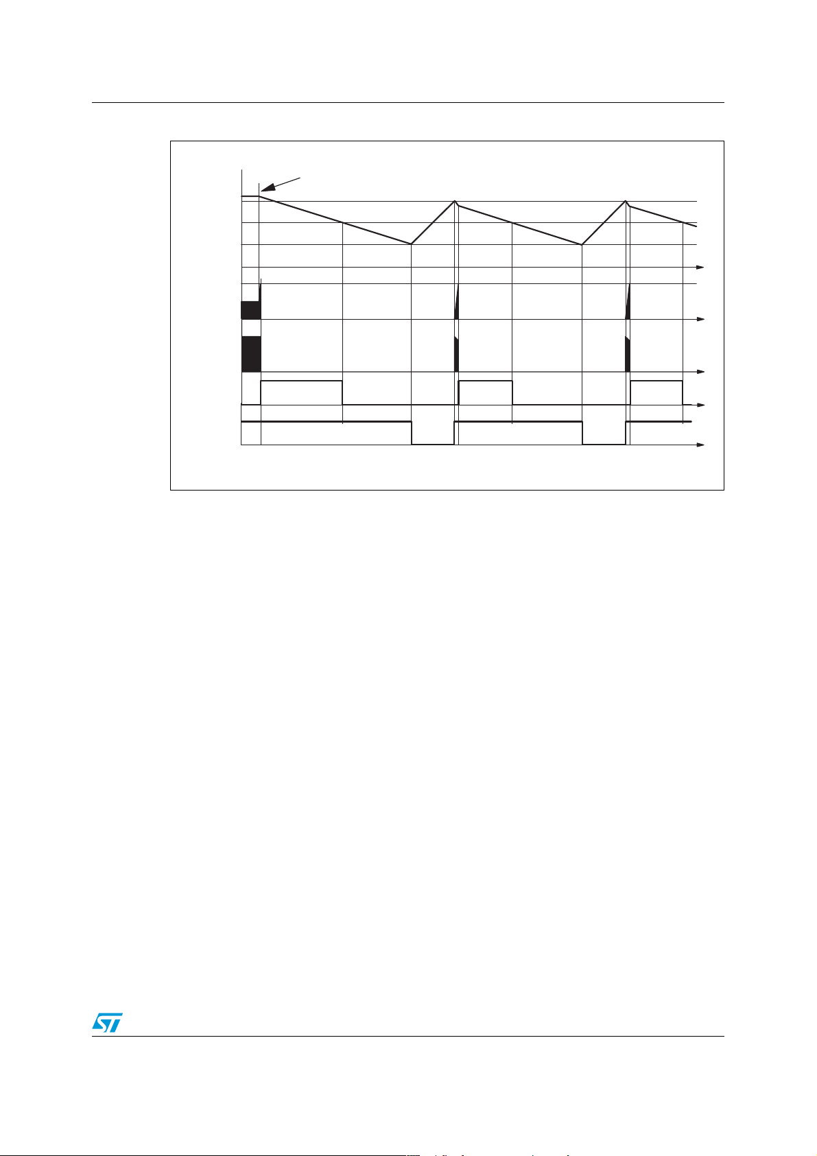
5.7 Hiccup-mode OCP
A third comparator senses the voltage on the current sense input and shuts down the device
if the voltage on the pin exceeds 1.5 V, a level well above that of the maximum overcurrent
setpoint (1 V). Such an anomalous condition is typically generated by either a short-circuit of
the secondary rectifier or a shorted secondary winding or a hard-saturated flyback
transformer.
Section 5.5: PWM
28/51 Doc ID 16610 Rev 2
Page 29
L6566BH Application information
Figure 18. Hiccup-mode OCP: timing diagram
Vcc
(pin 5)
Vc c
Vcc
Vc c
ON
OFF
restart
Secondary diode is shorted here
CS
V
(pin 7)
GD
(pin 4)
OCP latch
Vcc_OK
1.5 V
t
t
t
t
t
AM11494v1
To distinguish an actual malfunction from a disturbance (e.g. induced during ESD tests), the
first time the comparator is tripped the protection circuit enters a “warning state”. If in the
next switching cycle the comparator is not tripped, a temporary disturbance is assumed and
the protection logic is reset in its idle state; if the comparator is again tripped, a real
malfunction is assumed and the L6566BH is stopped. Depending on the time relationship
between the detected event and the oscillator, the device may occasionally stop after the
third detection.
This condition is latched as long as the device is supplied. While it is disabled, however, no
energy comes from the self-supply circuit; hence the voltage on the V
capacitor decays
CC
and crosses the UVLO threshold after some time, which clears the latch. The internal
startup generator is still off, and the V
before the V
capacitor is charged again and the device restarted. Ultimately, this results in
CC
voltage still needs to go below its restart voltage
CC
a low-frequency intermittent operation (Hiccup-mode operation), with very low stress on the
power circuit. This special condition is illustrated in the timing diagram of
Figure 18
.
5.8 Frequency modulation
To alleviate the converter’s EMI emissions and reduce cost and size of the line filter, it is
advantageous to modulate its switching frequency, so that the resulting spread-spectrum
action distributes the energy of each harmonic of the switching frequency over a number of
side-band harmonics. Their overall energy is unchanged but the individual amplitudes are
smaller. This is what naturally occurs with QR operation, due to the twice-mains-frequency
ripple appearing on the input bulk capacitor, which translates into different DCM-CCM
boundary frequencies.
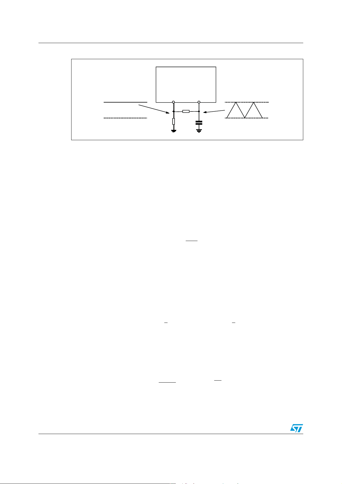
The L6566BH is provided with a dedicated pin, F
is selected.
Doc ID 16610 Rev 2 29/51
(6), to perform this function if FF mode
MOD
Page 30
Application information L6566BH
Figure 19. Frequency modulation circuit
L6566BH
1 V
0 V
With reference to
Figure 19
13
OSC
R
T
, the capacitor C
6
FMOD
R
MOD
MOD
C
MOD
is connected from F
1.5 V
0.5 V
to ground and is
MOD
AM11495v1
alternately charged and discharged between 0.5 and 1.5 V by internal current generators
sourcing and sinking the same current (three times the current defined by the resistor R
pin OSC). Therefore, the voltage across C
is determined by C
. By connecting a resistor R
MOD
is a symmetric triangle, whose frequency fm
MOD
MOD
from R
to OSC, the current
MOD
sourced by the OSC pin is modulated according to a triangular profile at a frequency f
R
is considerably higher than RT, as is normal, both fm and the symmetry of the triangle
MOD
on
T
. If
m
is little affected.
With this arrangement it is possible to set, nearly independently, the frequency deviation
∆f
and the modulating frequency fm, which define the modulation index:
sw
Equation 9
f∆
sw
=β
f
m
which is the parameter that the amplitude of the generated side-band harmonics depends
on.
The minimum frequency f
frequency f
centre value f
(occurring on the valley of the triangle) is symmetrically placed around the
sw_max
, so that:
sw
(occurring on the peak of the triangle) and the maximum
sw_min
Equation 10
1
swmin_sw
2
Then, R
oscillator block
is found from (5) (see
T
), while R
MOD
Section 5.2: Zero-current detection and triggering block;
and C
can be calculated as follows:
MOD
Equation 11
3
102
R
MOD
30/51 Doc ID 16610 Rev 2
⋅
=
f
∆
sw
C =
MOD
75
f
m
1
fff;fff ∆+=∆−=
swmax_swsw
sw
2
Page 31

L6566BH Application information
where ∆fsw and fm (in kHz, with C
MOD
achieve the best compromise between attenuation of peak EMI emissions and clean
converter operation.
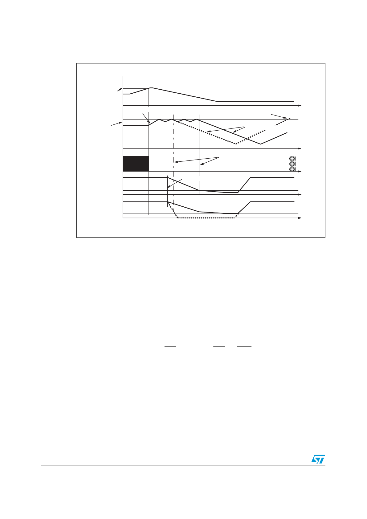
5.9 Latched disable function
The device is equipped with a comparator having the non-inverting input externally available
at the pin DIS (8) and with the inverting input internally referenced to 4.5 V. As the voltage
on the pin exceeds the internal threshold, the device is immediately shut down and its
consumption reduced to a low value.
The information is latched and it is necessary to let the voltage on the Vcc pin go below the
UVLO threshold to reset the latch and restart the device. To keep the latch supplied as long
as the converter is connected to the input source, the HV generator is activated periodically
so that Vcc oscillates between the startup threshold V
HV generator in this way cuts its power dissipation approximately by three (as compared to
continuous conduction) and keeps peak silicon temperature close to the average value.
To let the L6566BH restart, it is then necessary to disconnect the converter from the input
source. Pulling pin 16 (AC_OK) below the disable threshold (see
protection
cleared and a quicker restart is allowed as the input source is removed. This operation is
shown in the timing diagram of
This function is useful in order to implement a latched overtemperature protection very
easily by biasing the pin with a divider from VREF, where the upper resistor is an NTC
physically located close to a heating element like the MOSFET, or the transformer. The DIS
pin is a high impedance input, therefore it is prone to pick-up noise, which may lead to
undesired latch OFF of the device. It is possible to bypass the pin to ground with a small film
capacitor (e.g. 1-10 nF) to prevent any malfunctioning of this kind.
) stops the HV generator until Vcc falls below V
Figure 20
in nF and R
.
in kΩ) are selected by the user as to
MOD
CCON
and V
- 0.5 V. Activating the
ccON
Section 5.12: Brownout
CCrestart
, so that the latch can be
Doc ID 16610 Rev 2 31/51
Page 32
Application information L6566BH
Figure 20. Operation after latched disable activation: timing diagram
DIS
(pin 8)
4.5V
Vcc
Vcc
(pin 5)
Vcc
ON
Vcc
Vcc
GD
(pin 4)
HV generator is turned on
ON
-0.5
OFF
restart
Restart i s quicker
Disable latch is reset here
HV generator turn-on is disabled here
t
t
t
t
t
AM11496v1
HVstart
V
AC_OK
(pin 16)
Vin
Vth
Input source is removed here
5.10 Soft-start and delayed latched shutdown upon overcurrent
At device startup, a capacitor (CSS) connected between the SS pin (14) and ground is
charged by an internal current generator, I
clamped. During this ramp, the overcurrent setpoint progressively rises from zero to the
value imposed by the voltage on the VFF pin (15, see
latch and voltage feedforward blocks
); MOSFET conduction time increases gradually,
therefore controlling the startup inrush current. The time needed for the overcurrent setpoint
to reach its steady-state value, referred to as soft-start time, is approximately:
Equation 12
Css
T
SS
I
1SS
, from zero up to about 2 V where it is
SS1
Section 5.6: PWM comparator, PWM
V
VFF
3
⎞
⎟
⎟
⎠
⎛
Css
⎜
−==
)V(V
VFFcsx
1
⎜
I
⎝
1SS
During the ramp (i.e. until V
= 2 V) all the functions that monitor the voltage on the COMP
SS
pin are disabled.
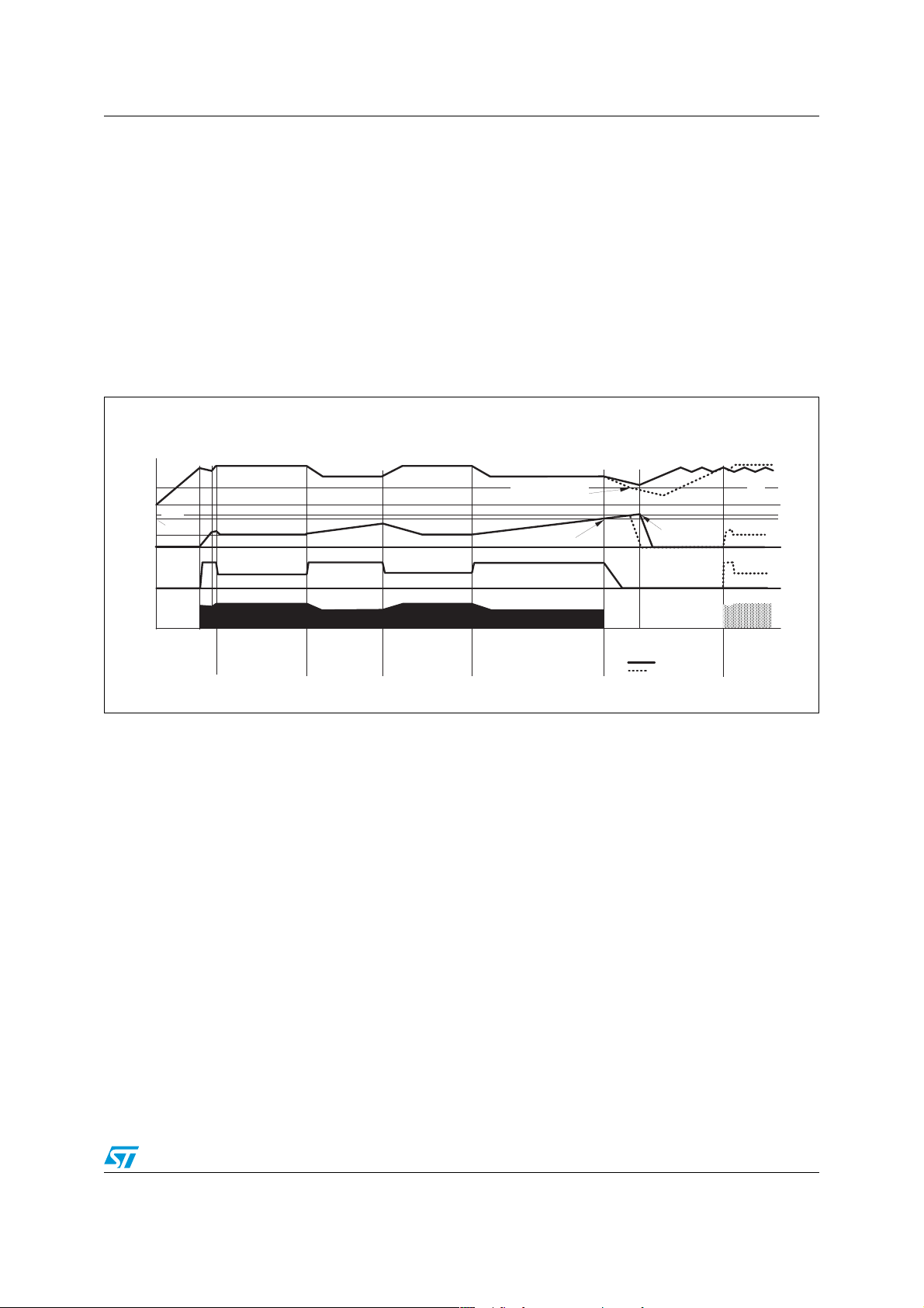
The soft-start pin is also invoked whenever the control voltage (COMP) saturates high,
which reveals an open loop condition for the feedback system. This condition very often
occurs at startup, but may be also caused by either a control loop failure or a converter
overload/short-circuit. A control loop failure results in an output overvoltage that is handled
by the OVP function of the L6566BH (see next section). In the case of QR operation, a
short-circuit causes the converter to run at a very low frequency, then with very low power
capability. This makes the self-supply system that powers the device unable to keep it
operating, so that the converter works intermittently, which is very safe. In the case of
32/51 Doc ID 16610 Rev 2
Page 33
L6566BH Application information
1
(
overload, the system has a power capability lower than that at nominal load but the output
current may be quite high and can overstress the output rectifier. In the case of FF operation
the capability is almost unchanged and both short-circuit and overload conditions are more
critical to handle.
The L6566BH, regardless of the operating option selected, makes it easier to handle such
conditions: the 2 V clamp on the SS pin is removed and a second internal current generator
I
= I
SS2
it is allowed to reach 2 V
resulting behavior is identical to that of short-circuit illustrated in
the result is identical to that of
/4 continues to charge CSS. As the voltage reaches 5 V the device is disabled, if
SS1
over 5 V, the device is latched off. In the former case the
BE
Figure 20
. See
Section 5.9: Latched disable function
Figure 7
; in the latter case
for
additional details.
Figure 21. Soft-start pin operation under different operating conditions and settings
Vcc
(pin 5)
SS
pin 14)
COMP
(pin 9)
Vcc falls below UVLO
5V+2Vbe
5V
2V
before latching off
here the IC
shuts down
here the IC
latches off
UVLO
t
t
GD
(pin 4)
START-UP
NORMAL
OPERATION
TEMPORARY
OVERLOAD
NORMAL
OPER ATION
OVERLOAD
SHUTDOWN
LATCH ED
AUTORESTART
RESTART
t
t
AM11497v
A diode, with the anode to the SS pin and the cathode connected to the VREF pin (10), is
the simplest way to select either auto-restart mode or latch-mode behavior upon
overcurrent. If the overload disappears before the Css voltage reaches 5 V, the I
SS2
generator is turned off and the voltage gradually brought back down to 2 V. Refer to
Section 6: Application examples and ideas (Ta bl e 7
) for additional information.
If latch-mode behavior is desired also for converter short-circuit, make sure that the supply
voltage of the device does not fall below the UVLO threshold before activating the latch.
Figure 21
shows soft-start pin behavior under different operating conditions and with
different settings (latch-mode or auto-restart).
Note: Unlike other PWM controllers provided with a soft-start pin, in the L6566BH grounding the
SS pin does not guarantee that the gate driver is disabled.
5.11 OVP block
The OVP function of the L6566BH monitors the voltage on the ZCD pin (11) in MOSFET
OFF-time, during which the voltage generated by the auxiliary winding tracks the converter’s
output voltage. If the voltage on the pin exceeds an internal 5 V reference, a comparator is
triggered, an overvoltage condition is assumed and the device is shut down. An internal
current generator is activated that sources 1 mA out of the VFF pin (15). If the VFF voltage
Doc ID 16610 Rev 2 33/51
Page 34
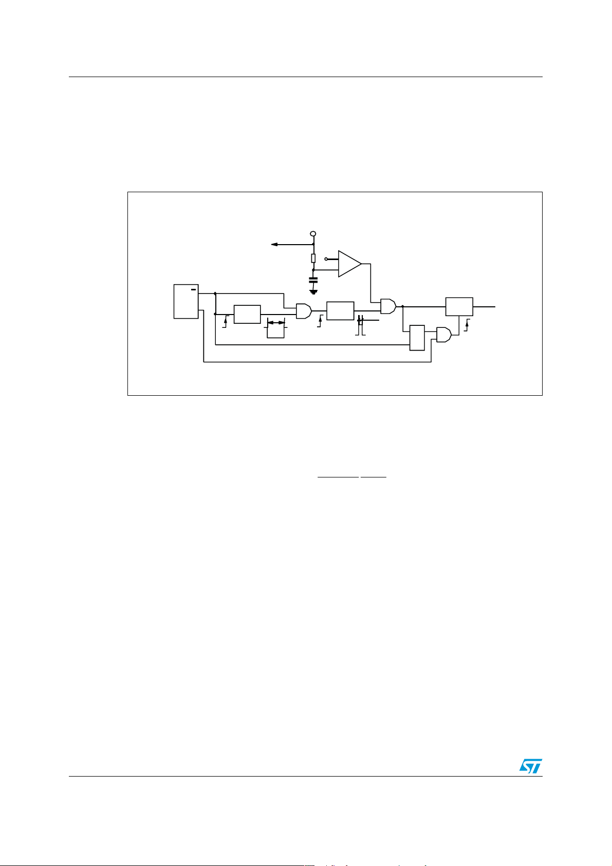
Application information L6566BH
is allowed to reach 2 Vbe over 5 V, the L6566BH is latched off. See
disable function
externally connected to pin 15 is so low that the 5+2 V
for more details on IC behavior under these conditions. If the impedance
threshold cannot be reached or if
BE
Section 5.9: Latched
some means is provided to prevent that, the device is able to restart after the Vcc has
dropped below 5 V. Refer to
Section 6: Application examples and ideas (Ta bl e 7
) for
additional information.
Figure 22. OVP function: internal block diagram
ZCD
2 µs
11
40kW
5pF
5 V
Monostable
-
+
M2
STROB E
0.5 µs
COUT
OVP
FF
R Q1
S
L6566BH
Fault
2-bit
counter
Counter
reset
AM11498v1
PWM latch
QQSR
to triggering
block
Monostable
M1
The ZCD pin is connected to the auxiliary winding through a resistor divider R
Figure 8
). The divider ratio k
OVP
= R
Z2
/ (R
+ RZ2) is chosen equal to:
Z1
, RZ2 (see
Z1
Equation 13
OVP
Ns
Naux
where Vout
=
5
Vout
k
OVP
is the output voltage value that is to activate the protection, Ns the turn
OVP
number of the secondary winding, and Naux the turn number of the auxiliary winding.
34/51 Doc ID 16610 Rev 2
Page 35
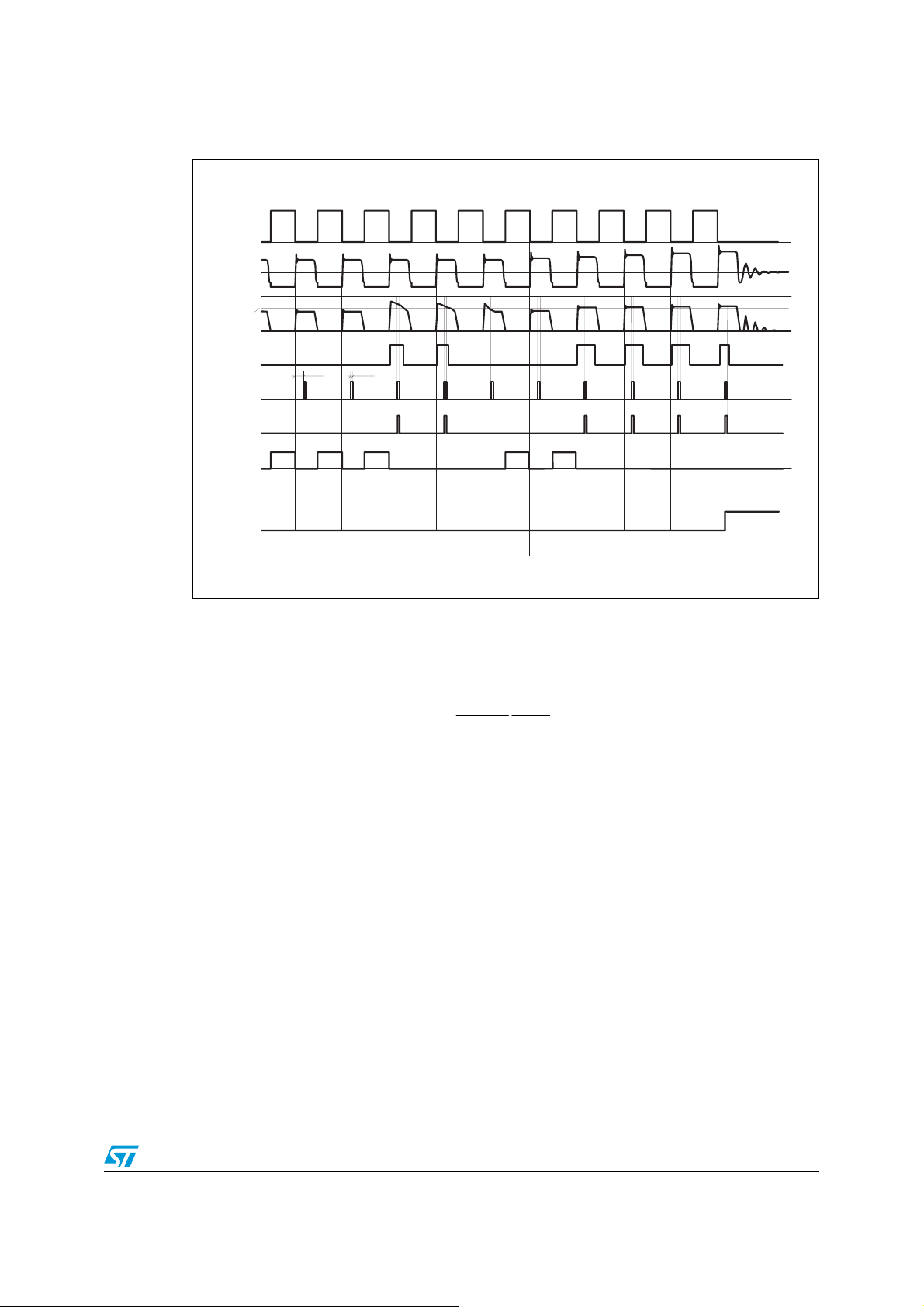
L6566BH Application information
Figure 23. OVP function: timing diagram
GD
(pin 4)
Vaux
0
ZCD
(pin 11)
5V
COUT
STROBE
OVP
COUNTER
RESET
COUNTER
STATUS
FAULT
The value of R
2 µs 0.5 µ s
00 00 11 22 00
is such that the current sourced by the ZCD pin be within the rated
Z1
capability of the internal clamp:
Equation 14
t
t
t
t
t
t
11 22 33 40
ERULIAF POOL KCABDEEFECNABRUTSID YRAROPMETNOITAREPO LAMRON
t
t
t
AM11499v1
Naux
1
where Vin
max
winding. See
≥
R
1Z
3
−
⋅
103
is the maximum DC input voltage and Ns the turn number of the primary
Section 5.2: Zero-current detection and triggering block; oscillator block
Np
Vin
max
additional details.
To reduce sensitivity to noise and prevent the latch from being erroneously activated, firstly
the OVP comparator is active only for a small time frame (typically, 0.5 µs) starting 2 µs after
MOSFET turn-off, to reject the voltage spike associated to the positive-going edges of the
voltage across the auxiliary winding Vaux; secondly, to stop the L6566BH, the OVP
comparator must be triggered for four consecutive switching cycles. A counter, which is
reset every time the OVP comparator is not triggered in one switching cycle, is provided for
this purpose.
Figure 22
shows the internal block diagram, while the timing diagrams in
Figure 23
illustrate
the operation.
Note: To use the OVP function effectively, i.e. to ensure that the OVP comparator is always
interrogated during MOSFET OFF-time, the duty cycle D under open loop conditions must
fulfill the following inequality:
for
Doc ID 16610 Rev 2 35/51
Page 36
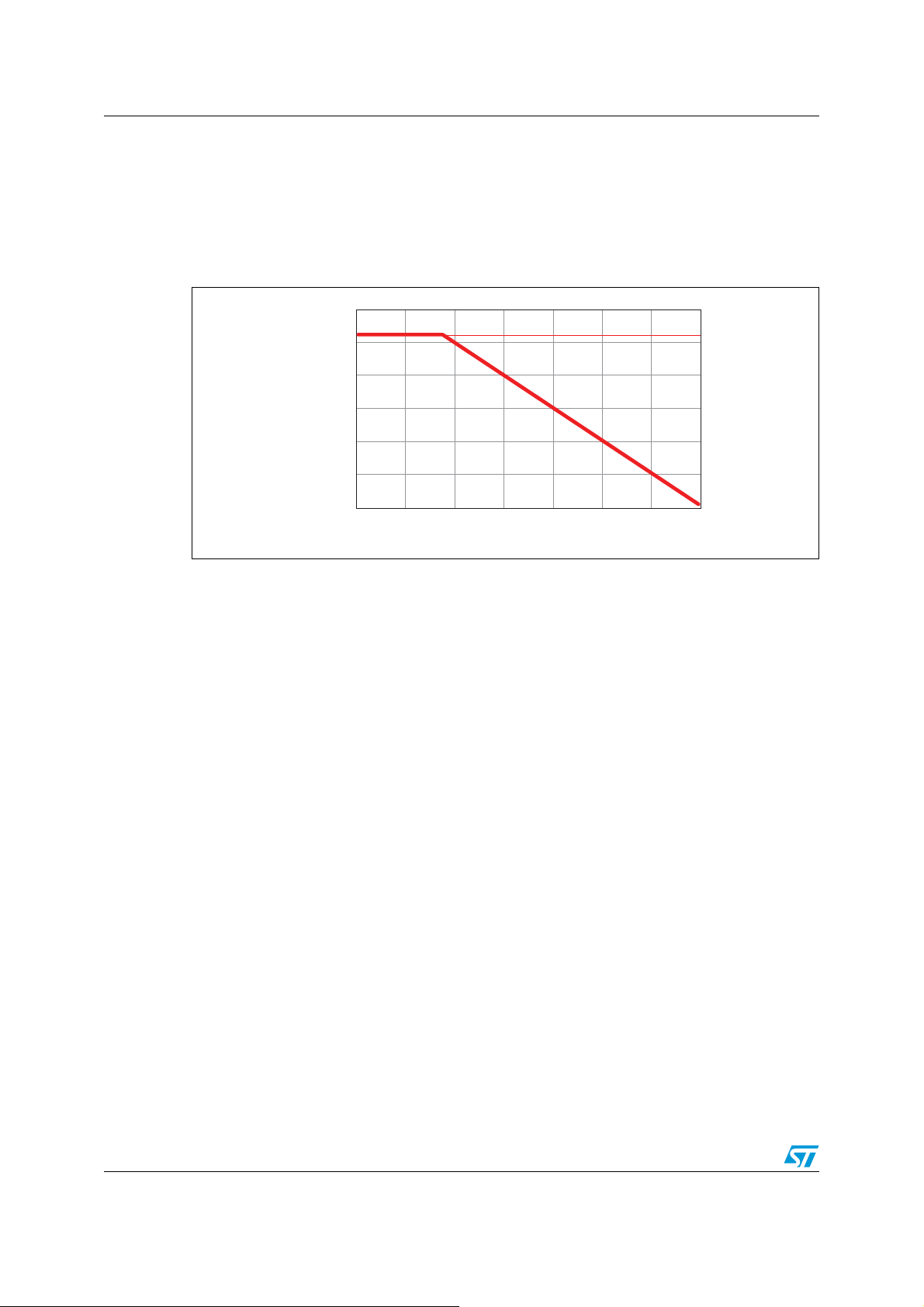
Application information L6566BH
1
Equation 15
1fTD
≤+
sw2BLANK
where T
BLANK2
= 2 µs; this is also illustrated in the diagram of
Figure 24. Maximum allowed duty cycle vs. switching frequency for correct OVP
detection
0.8
0.7
0.6
0.5
Dmax
0.4
0.3
0.2
5.1041.1051.5.1052.1052.5.1053.1053.5.1054.10
5.12 Brownout protection
Brownout protection is basically a not-latched device shutdown function activated when a
condition of mains undervoltage is detected. There are several reasons why it may be
desirable to shut down a converter during a brownout condition, which occurs when the
mains voltage falls below the minimum specification of normal operation.
fsw [ H z ]
Figure 24
.
0.725
5
AM11500v
Firstly, a brownout condition may cause overheating of the primary power section due to an
excess of RMS current. Secondly, spurious restarts may occur during converter power
down, therefore causing the output voltage to not decay to zero monotonically.
L6566BH shutdown upon brownout is accomplished by means of an internal comparator, as
shown in the block diagram of
Figure 25
, which shows the basic usage. The inverting input
of the comparator, available on the AC_OK pin (16), is supposed to sense a voltage
proportional to the RMS (peak) mains voltage; the non-inverting input is internally
referenced to 0.485 V with 35 mV hysteresis. If the voltage applied on the AC_OK pin before
the device starts operating does not exceed 0.485 V or if it falls below 0.45 V while the
device is running, the AC_FAIL signal goes high and the device shuts down, with the softstart capacitor discharged and the gate-drive output low. Additionally, if the device has been
latched off by some protection function (testified by Vcc oscillating between V
V
- 0.5 V) the AC_OK voltage falling below 0.45 V clears the latch. This may allow a
CCON
quicker restart as the input source is removed.
While the brownout protection is active the startup generator keeps on working but, there
being no PWM activity, the Vcc voltage continuously oscillates between the startup and the
HV generator restart thresholds, as shown in the timing diagram of
36/51 Doc ID 16610 Rev 2
Figure 25
CCON
.
and
Page 37
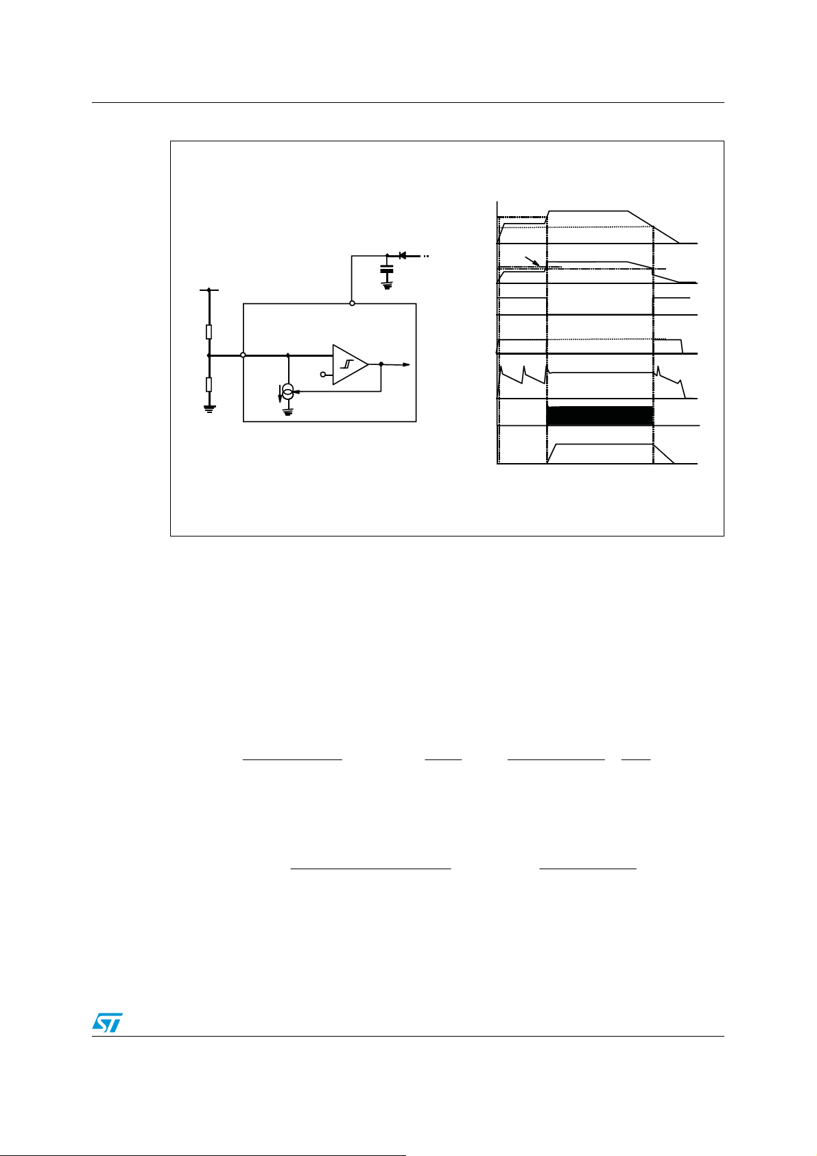
L6566BH Application information
Figure 25. Brownout protection: internal block diagram and timing diagram
Sensed volt age
ON
Vsen
OFF
Vsen
Sensed
voltage
H
R
L
R
AC_OK
L6566BH
16
15 µA
0.485V
0.45V
Vcc
VAC_OK
5
-
+
AC_FAI L
(pi n 16)
AC_FAI L
HYS
I
15 µA
Vcc
(pin 5)
GD
(pin 4)
Vout
0.485V
t
0.45V
t
t
t
t
t
t
AM11501v1
The brownout comparator is provided with current hysteresis in addition to voltage
hysteresis: an internal 15 µA current sink is ON as long as the voltage applied on the
AC_OK pin is such that the AC_FAIL signal is high. This approach provides an additional
degree of freedom: it is possible to set the ON threshold and the OFF threshold separately
by properly choosing the resistors of the external divider (see below). With just voltage
hysteresis, on the other hand, fixing one threshold automatically fixes the other one
depending on the built-in hysteresis of the comparator.
With reference to
(Vsen
) and OFF (Vsen
ON
Figure 25
OFF
, the following relationships can be established for the ON
) thresholds of the sensed voltage:
Equation 16
which, solved for R
485.0Vsen
−
ON
R
H
and RL, yields:
H
485.0
6
−
1015
+⋅=
R
L
OFF
R
−
45.0Vsen
45.0
=
R
LH
Equation 17
Vsen078.1Vsen
⋅−
R
=
H
−
1015
⋅
OFFON
6
RR;
=
HL
OFF
45.0
45.0Vsen
−
Doc ID 16610 Rev 2 37/51
Page 38
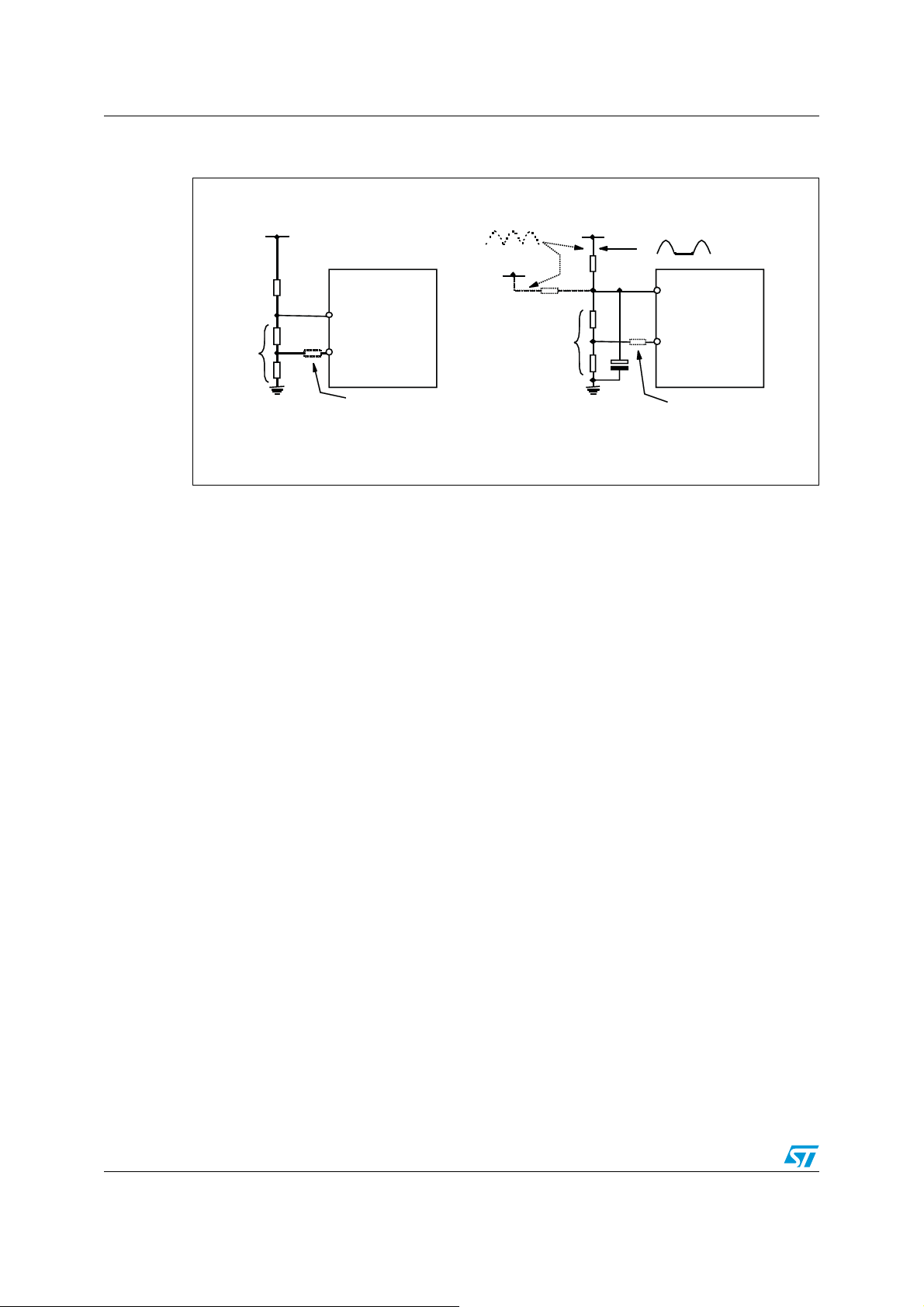
Application information L6566BH
Figure 26. Voltage sensing techniques to implement brownout protection with the
L6566BH
HV Inp ut bus
H
R
L1
R
L
R
L2
R
AC mains (N/L)
AC_OK
16
VFF
L6566BH
15
Optional for
OVP settings
a) b)
AC mains (L/N)
H
R
H
R
L
R
AC_OK
16
L1
R
VFF
L2
R
F
C
L6566BH
15
Optionalfor
OVP settings
AM11502v1
It is usually convenient to use a single divider to bias both the AC_OK and the VFF pins, as
shown in
is lower than that on the AC_OK pin. Once R
above, and k
Figure 26
: this is possible because in all practical cases the voltage on the VFF pin
and RL have been found, as suggested
, either calculated from (6) or (8) or experimentally found, RL is split as:
opt
H
Equation 18
()
RRR;RRkR −=+=
2LL1LHLopt2L
Circuit a) senses the input voltage bus (across the bulk capacitor, downstream of the bridge
rectifier); in this case, for a proper operation of the brownout function, Vsen
than the peak voltage at minimum mains and Vsen
lower than the minimum voltage on
OFF
must be lower
ON
the input bulk capacitor at minimum mains and maximum load considering, if necessary,
holdup requirements during mains missing cycles as well. Brownout level is loaddependent. In case of latched shutdown, when the input source is removed it is necessary
to wait until the bulk capacitor voltage falls below the start voltage of the HV generator
V
in order for the unit to restart, which may take up to several seconds.
HVstart
Circuit b) senses the mains voltage directly, upstream of the bridge rectifier. It can be
configured either for half-wave sensing (only the line/neutral wire is sensed) or full-wave
sensing (both neutral and line are sensed); in the first case, assuming C
is large enough,
F
the sensed voltage is equal to 1/π the peak mains voltage, while in the second case it is
equal to 2/π the peak mains voltage. C
needs to be quite a big capacitor (in the uF) to have
F
small residual ripple superimposed on the DC level; as a rule-of-thumb, use a time constant
R
at least 4-5 times the maximum line cycle period in case of half-wave sensing, 2-3
L ·CF
times in case of full-wave sensing. Then fine tune if needed, considering also transient
conditions such as mains missing cycles. Brownout level does not depend on the load.
When the input source is removed, C
is discharged after some ten ms then this circuit is
F
suitable for a quick restart after a latched shutdown.
The AC_OK pin is a high impedance input connected to high value resistors, therefore it is
prone to pick-up noise, which might alter the OFF threshold when the converter is running or
lead to undesired switch-off of the device during ESD tests. It is possible to bypass the pin to
ground with a small film capacitor (e.g. 1-10 nF) to prevent any malfunctioning of this kind.
38/51 Doc ID 16610 Rev 2
Page 39
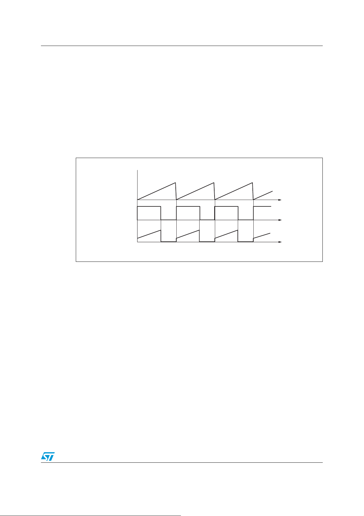
L6566BH Application information
The voltage on the pin is clamped upwards at about 3.15 V; then, if the function is not used,
the pin must be connected to Vcc through a resistor (220 to 680 kΩ).
5.13 Slope compensation
The MODE/SC pin (12), when not connected to VREF, provides a voltage ramp during
MOSFET ON-time synchronous to that of the internal oscillator sawtooth, with 0.8 mA
minimum current capability. This ramp is intended for implementing additional slope
compensation on current sense. This is needed to avoid the sub-harmonic oscillation that
arises in all peak-current-mode-controlled converters working at fixed frequency in
continuous conduction mode with a duty cycle close to or exceeding 50%.
Figure 27. Slope compensation waveforms
Internal
oscillator
GD
(pin 4)
MOD E/ SC
(pin 12)
t
t
t
AM11503v1
The compensation is realized by connecting a programming resistor between this pin and
the current sense input (pin 7, CS). The CS pin must be connected to the sense resistor with
another resistor to make a summing node on the pin. Since no ramp is delivered during
MOSFET OFF-time (see
Figure 27
), no external component other than the programming
resistor is needed to ensure a clean operation at light loads.
Note: The addition of the slope compensation ramp reduces the available dynamics of the current
signal; thereby, the value of the sense resistor must be determined taking this into account.
Note also that the burst-mode threshold (in terms of power) is slightly changed.
If slope compensation is not required with FF operation, the pin is left floating.
5.14 Summary of L6566BH power management functions
The device is provided with a number of power management functions: multiple operating
mode upon loading conditions and protection functions. To help the user familiarize
themselves with these functions, in the following tables, all themes are summarized with
their respective activation mechanism and the resulting status of the most important pins.
This can be useful not only for a correct use of the IC but also for diagnostic purposes:
especially at the prototyping/debugging stage, it is quite common to come across unwanted
activation of some function, and these tables can be used as a kind of quick troubleshooting
guide.
Doc ID 16610 Rev 2 39/51
Page 40

40/51 Doc ID 16610 Rev 2
Table 5. L6566BH light load management features
Application information L6566BH
Feature Description Caused by
Burst
mode
Controlled ON-OFF
operation for low power
consumption at light load
V
COMP
V
COMPBM - Hys
Table 6. L6566BH protection
Protection Description Caused by
V
ZCD>VZCDth
OVP
OLP
Short-
circuit
protection
2nd OCP
Output overvoltage
protection
Output overload
protection
Output short-circuit
protection
Transformer saturation
or shorted secondary
diode protection
consecutive
switching cycles
VFF > VFFlatch Latched 13.5 0.33 0 0 0 0 0 0
=V
V
COMP
VSS > V
V
COMP
VSS > V
V
COMP
VSS > V
V
COMP
VSS > V
V
CS
> V
SSDIS
=V
SSLAT
=V
SSDIS
=V
SSLAT
CSDIS
COMPHi
COMPHi
COMPHi
COMPHi
for 2-3
consecutive
switching cycles
<
Pulse skipping
behavior
for 4
(4)
(6)
IC
behavior
operation
IC
Auto
restart
Auto
restart
(1)
(2)
VCC_restart
(V)
N.A. 1.34 mA 5 Unchanged
Vcc
restart
(V)
IC Iq
(mA)
VREF
52.25
51.465
Consump.
(Iqdis,mA)
(V)
Unchanged
(6)
(6)
<V
VREF
SS
(6)
VSS
SSLAT
(V)
(3)
SS
VCOMP
(V)
VCOMP
(V)
V
COMPBM-HYS
V
COMPBM
OSC
(V)
FMOD VFF
OSC
to
0 0 0 Unchanged
V
COMPHi
(6)
0 0 Unchanged
(V)
0/1 0
Latched 13.5 0.33 0 0 0 0 0 0
Auto
restart
51.460
<V
V
SS
SSLAT
V
(6)
COMPHi
(5)
0 Unchanged
Latched 13.5 0.33 0 0 0 0 0 0
Latched 5 0.33 0 0 0 0 0 0
FMOD
Page 41

41/51 Doc ID 16610 Rev 2
Table 6. L6566BH protection (continued)
Application information L6566BH
Protection Description Caused by
IC
behavior
Externally settable
Latched 13.5 0.33 0 0 0 0 0 0
Auto
(5)
restart
Auto
restart
Latched 13.5 0.33 0 0 0 0 0 0
Auto
restart
Latched 10 0.33 0 0 0 0 0 0
Auto
restart
.
REF
falls below UVLO (
cc
OTP
overtemperature
protection
V
DIS>VOTP
Internal shutdown Tj > 160 oC
Brownout
Reference
drift
Shutdown1 Gate driver disable V
Shutdown2 Shutdown by V
Adaptive
UVLO
1. Use one external diode from VFF (#15) to AC_OK (#16), cathode to AC_OK.
2. Use one external diode from SS (#14) to V
3. If C
4. If C
5. When T
6. Discharged to zero by V
Mains undervoltage
protection
drift protection V
V
REF
COMP
Shutdown by V
below V
V
ccoff
threshold at light
ccoff
going
cc
(lowering of
load)
and the Vcc capacitor are such that Vcc falls below UVLO before latch tripping (
ss
and the Vcc capacitor are such that the latch is tripped before V
ss
< 110 oC.
J
going below UVLO.
cc
low
V
< V
AC_OK
> V
REF
FF
V
COMP
V
COMPOFF
V
cc
(
VCOMP
V
COMPL
V
cc
(
VCOMP
V
COMPO
REF
ov
> V
off
<
< 9.4 V
>
)
< 7.2 V
>
)
(#10), cathode to V
th
Vcc
restart
(V)
IC Iq
(mA)
VREF
(V)
SS
VCOMP
(V)
OSC
(V)
FMOD VFF
50.330 0 0 0 0 0
5 0.33 0 0 0 0 0 Unchanged
5 2.5 5 Unchanged Unchanged 1 Unchanged Unchanged
0.18m
5 V
A
Figure 21
00 000 0
).
Figure 21
).
Page 42

Application information L6566BH
It is worth remembering that “auto-restart” means that the device works intermittently as
long as the condition that is activating the function is not removed; “Latched” means that the
device is stopped as long as the unit is connected to the input power source and the unit
must be disconnected for some time from the source in order for the device (and the unit) to
restart. Optionally, a restart can be forced by pulling the voltage of pin 16 (AC_OK) below
0.45 V.
42/51 Doc ID 16610 Rev 2
Page 43
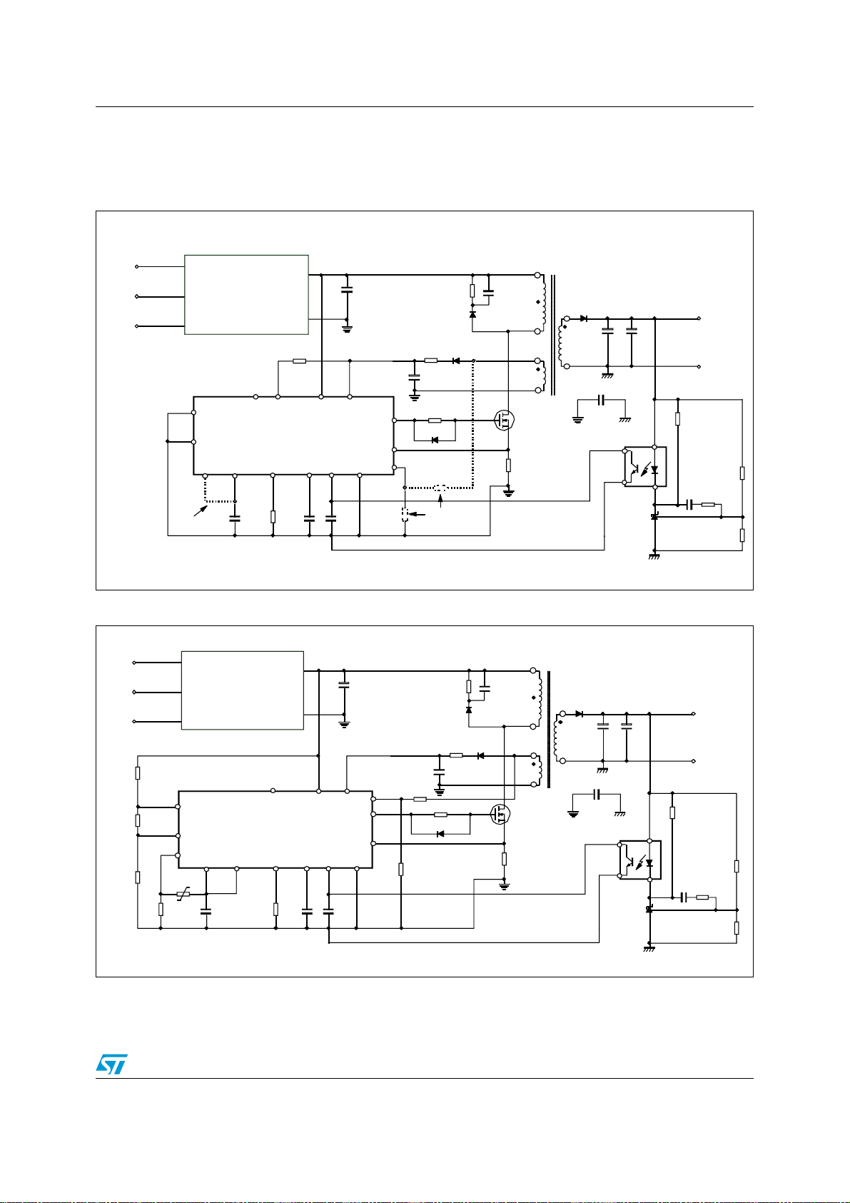
L6566BH Application examples and ideas
6 Application examples and ideas
Figure 28. Typical low-cost application schematic
6IN
PHASERECTIFIER
%-)FILTER
$)3
6&&
62%&-/$%3#
/PTIONALFOR
12OPERATION
# 2
2K
)#
,"(
/3#
#
#
2
#
6CC!#?/+
(63&-/$
#/-0
33
'.$
#
'$
#3
:#$
2
$
/PTIONALFOR
12OPERATION
4
2
$
$
#
1
2
$
#!"
#9
6OUT
2
)#
4,
2
#
2
2
!-V
2
!#?/+
6&&
$)
3
.4#
PHASERECTIFIER
%-)FILTER
&-/$
,"(
62%&
-/$%3#
# 2
(63
)#
33
/3#
#
#/-0
#
4
#
6CC
:#$
'$
#3
'.$
2
#
2
2
$.
2
$
2
$
.
#
1
2
Figure 29. Typical full-feature application schematic (QR operation)
6IN
2
2
2
$
#!"
#9
)#0#!
4,
6OUT
2
2
#
2
2
!-V
Doc ID 16610 Rev 2 43/51
Page 44
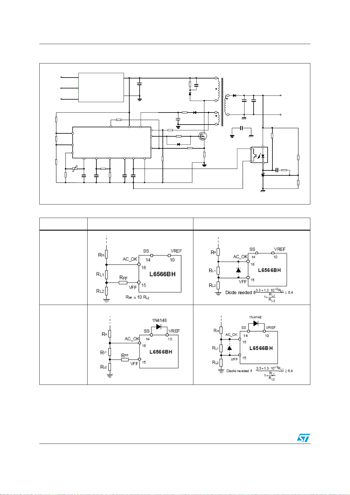
Application examples and ideas L6566BH
Figure 30. Typical full-feature application schematic (FF operation)
2
2
2
Table 7. External circuits that determine IC behavior upon OVP and OCP
4
(63
#/-0
#
6CC
:#$
'$
#3
'.$
#
$)3
.4#
# 2
PHASERECTIFIER
%-)FILTER
-/$%3#
)#
,"(
62%&
#
&-/$
2
/3#
2
33
#
6IN
!#?/+
6&&
2
#
2
2
2
$.
2
$
2
2
$
.
#
1
2
$
#!"
#9
OVP latched OVP auto-restart
)#0#!
4,
6OUT
2
2
#
2
2
!-V
OCP latched
OCP auto-restart
44/51 Doc ID 16610 Rev 2
Page 45
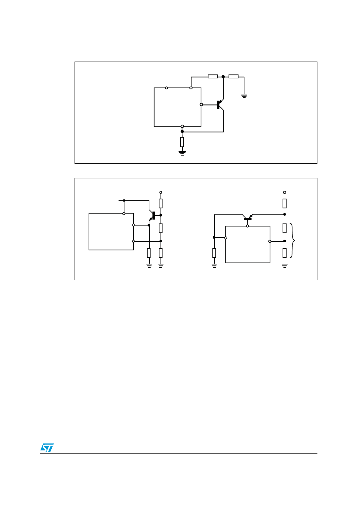
L6566BH Application examples and ideas
Figure 31. Frequency foldback at light load (FF operation)
R1
MODE/SC
12
L6566BH
OSC
T
R
Vref
10
COMP
9
13
BC857C
Figure 32. Latched shutdown upon mains overvoltage
Vin
Vcc
L6566BH
BC847
5
15
DIS
8
VFF
>10 R q
DIS
R2
8
BC857
Vref
10
L6566BH
15
VFF
AM11504v1
Vin
Rq
AM11504v1
Doc ID 16610 Rev 2 45/51
Page 46
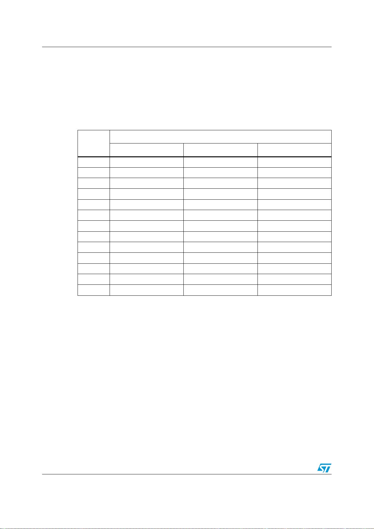
Package mechanical data L6566BH
7 Package mechanical data
In order to meet environmental requirements, ST offers these devices in different grades of
®
ECOPACK
packages, depending on their level of environmental compliance. ECOPACK
specifications, grade definitions and product status are available at: www.st.com. ECOPACK
is an ST trademark.
Table 8. SO16N mechanical data
mm
Dim.
Min. Typ. Max.
A 1.75
A1 0.10 0.25
A2 1.25
b0.31 0.51
c0.17 0.25
D 9.80 9.90 10.00
E5.806.006.20
E1 3.80 3.90 4.00
e1.27
h0.25 0.50
L0.40 1.27
k0 8°
ccc 0.10
46/51 Doc ID 16610 Rev 2
Page 47
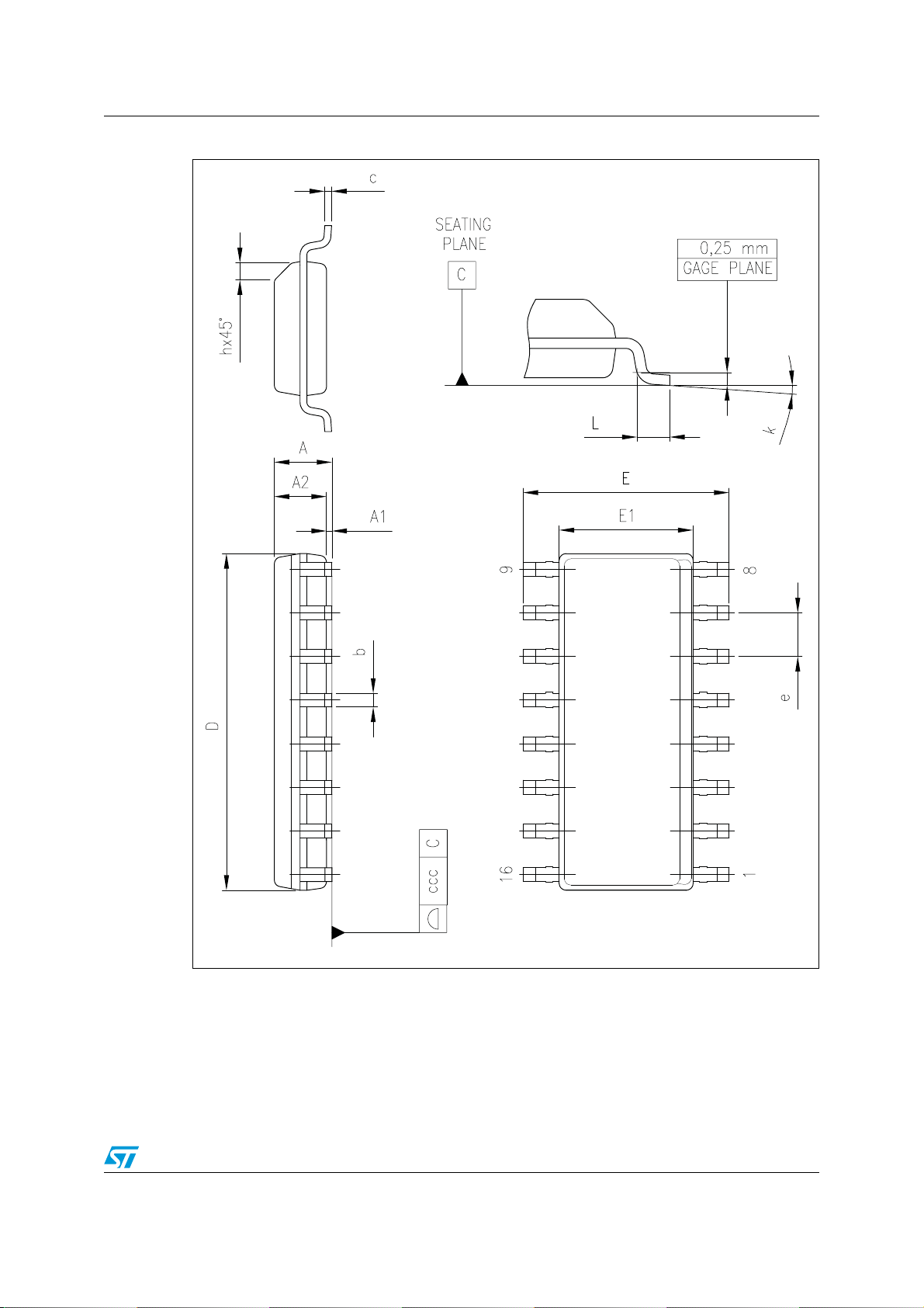
L6566BH Package mechanical data
Figure 33. SO16N package drawing
0016020_F
Doc ID 16610 Rev 2 47/51
Page 48
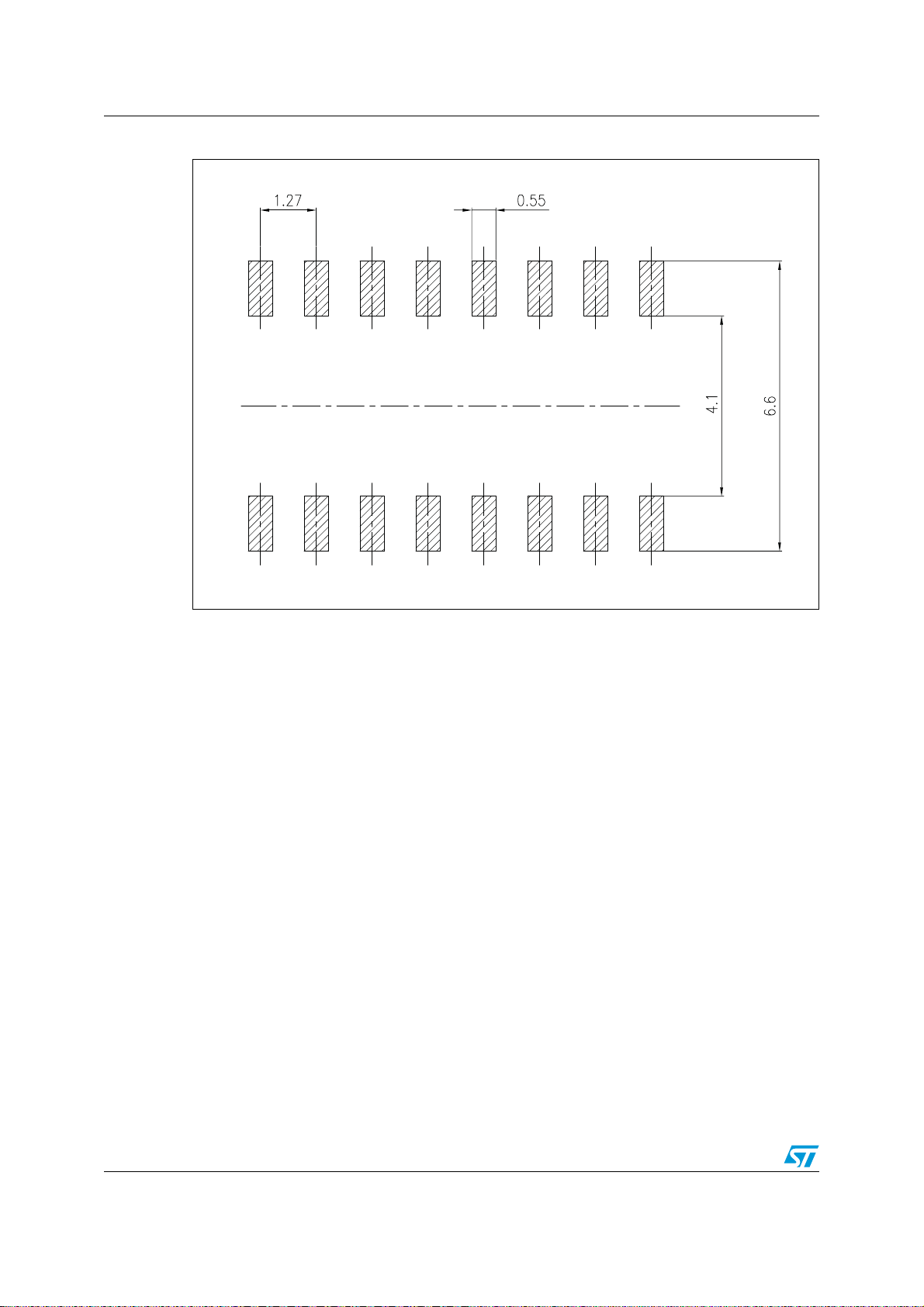
Package mechanical data L6566BH
Figure 34. Recommended footprint (dimensions are in mm)
48/51 Doc ID 16610 Rev 2
Page 49

L6566BH Order codes
8 Order codes
Table 9. Order codes
Order codes Package Packaging
L6566BH SO16N Tube
L6566BHTR SO16N Tape and reel
Doc ID 16610 Rev 2 49/51
Page 50

Revision history L6566BH
9 Revision history
Table 10. Document revision history
Date Revision Changes
30-Nov-2009 1 First release
Updated internal voltage reference: typical value from 800 V to 840 V
in the entire document.
Ta bl e 2
and
Table 4
16-Apr-2012 2
Updated:
Added footnote 4 on
Updated
Minor text changes.
Figure 8
. and
Ta b l e 4
.
.
Section 7: Package mechanical data
.
50/51 Doc ID 16610 Rev 2
Page 51

L6566BH
Please Read Carefully:
Information in this document is provided solely in connection with ST products. STMicroelectronics NV and its subsidiaries (“ST”) reserve the
right to make changes, corrections, modifications or improvements, to this document, and the products and services described herein at any
time, without notice.
All ST products are sold pursuant to ST’s terms and conditions of sale.
Purchasers are solely responsible for the choice, selection and use of the ST products and services described herein, and ST assumes no
liability whatsoever relating to the choice, selection or use of the ST products and services described herein.
No license, express or implied, by estoppel or otherwise, to any intellectual property rights is granted under this document. If any part of this
document refers to any third party products or services it shall not be deemed a license grant by ST for the use of such third party products
or services, or any intellectual property contained therein or considered as a warranty covering the use in any manner whatsoever of such
third party products or services or any intellectual property contained therein.
UNLESS OTHERWISE SET FORTH IN ST’S TERMS AND CONDITIONS OF SALE ST DISCLAIMS ANY EXPRESS OR IMPLIED
WARRANTY WITH RESPECT TO THE USE AND/OR SALE OF ST PRODUCTS INCLUDING WITHOUT LIMITATION IMPLIED
WARRANTIES OF MERCHANTABILITY, FITNESS FOR A PARTICULAR PURPOSE (AND THEIR EQUIVALENTS UNDER THE LAWS
OF ANY JURISDICTION), OR INFRINGEMENT OF ANY PATENT, COPYRIGHT OR OTHER INTELLECTUAL PROPERTY RIGHT.
UNLESS EXPRESSLY APPROVED IN WRITING BY TWO AUTHORIZED ST REPRESENTATIVES, ST PRODUCTS ARE NOT
RECOMMENDED, AUTHORIZED OR WARRANTED FOR USE IN MILITARY, AIR CRAFT, SPACE, LIFE SAVING, OR LIFE SUSTAINING
APPLICATIONS, NOR IN PRODUCTS OR SYSTEMS WHERE FAILURE OR MALFUNCTION MAY RESULT IN PERSONAL INJURY,
DEATH, OR SEVERE PROPERTY OR ENVIRONMENTAL DAMAGE. ST PRODUCTS WHICH ARE NOT SPECIFIED AS "AUTOMOTIVE
GRADE" MAY ONLY BE USED IN AUTOMOTIVE APPLICATIONS AT USER’S OWN RISK.
Resale of ST products with provisions different from the statements and/or technical features set forth in this document shall immediately void
any warranty granted by ST for the ST product or service described herein and shall not create or extend in any manner whatsoever, any
liability of ST.
ST and the ST logo are trademarks or registered trademarks of ST in various countries.
Information in this document supersedes and replaces all information previously supplied.
The ST logo is a registered trademark of STMicroelectronics. All other names are the property of their respective owners.
© 2012 STMicroelectronics - All rights reserved
STMicroelectronics group of companies
Australia - Belgium - Brazil - Canada - China - Czech Republic - Finland - France - Germany - Hong Kong - India - Israel - Italy - Japan -
Malaysia - Malta - Morocco - Philippines - Singapore - Spain - Sweden - Switzerland - United Kingdom - United States of America
www.st.com
Doc ID 16610 Rev 2 51/51
 Loading...