

Page 1
L6515
DUAL DC-MOTOR POSITIONING SYSTEM
ADVANCE DATA
PRECISE OPERATION ALSO WITH LOW
COST OPTICALENCODER
PWM - OUTPUT FOR DIGITAL SWITCHED
POWERBRIDGES
DIRECTION INDICATOR FOR EASY POSITIONCOUNTING WITH µP
EXTERNAL LOOP GAIN AND TRANSFER
FUNCTIONALADJUSTMENT
PARALLEL ADDRESSED INPUTS WITH
LATCH
44 LEAD PLCC PACKAGE
DESCRIPTION
The L6515 is a monolithic integrated circuit in
BCD-Technologyassembledina PLCC-44plastic
chipcarrier.
The device contains all functions for a complete
dual DC-Motor positioning system. For the motor
driver stage only digital switched bridges are
needed.
Useful are L293E, L298, L6203 and L6202. The
device is intended to drive DC-Motors in typewriters, printers, plotters and general purpose industrialapplications.
This isadvanced information on anew product now in development or undergoing evaluation. Details are subject tochange without notice.
May 1994
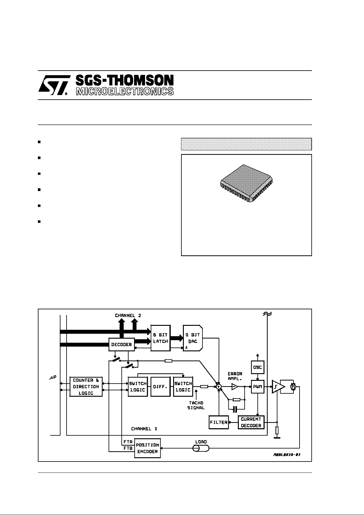
SYSTEM BLOCK DIAGRAM (ONECHANNEL)
PLCC44
ORDERING NUMBER: L6515
MULTIPOWERBCD TECHNOLOGY
1/13
Page 2
SYSTEM DESCRIPTION
The L6515 is intended to be used as a microprocessorcontrolledpositioningsystem.
For the motor driver stage only digital operating
bridgesareneededl ikeL293E,L298,L6203,L6202.
The system operates in two modes to achieve
high-speed,high-accurancy positioning.
Speed commands for the system originate in the
microprocessor. It is continuouslyupdated on the
motor position by means of pulses from the controller chip, which in turn gets its information from
the encoder. From this basic input, the microprocessor computes a 6-bit control word that sets the
systemspeed anddirectiondependenton the distance to travel.
When the motor is stopped and the microprocessor orders it to a new position, the system oper-
ates initially in an open-loop configuration as
there is no feedback from the tachometer generator.Therefore maximumcurrentis fed to themotor. As maximum speed is reached, the tachometer chip output backs off the processors signal
thus reducing acceleratingtorque.Themotor continues to run at top speed but under closed-loop
control.
As a target position is approached,the microprocessor lowers the value of the speed-demand
word; this reduces the voltage at the main summing point, in effect braking the motor. The braking is appliedprogressively until the motor is running at minimum speed.
At that time, the microprocessor orders a switch
to the position mode, and within 3 to 4ms the
power stage drives the motor to a null position,
whereit is held by electronic ”detening”.
Symbol Parameter Value Unit
V
S
Supply Voltage 12 V
V
IA
Analog Inputs Voltage -0.3 to 7 V
V
IL
Logic Inputs Voltage -0.3 to 7 V
V
O
Open Collector Output Current 12 V
I
O
Open Collector Current 10 mA
I
Z
Zener Current 20 mA
T
stg
, Tj Storage Temperature -40to 150 °C
T
amb
Operative Ambient Temperature 0 to 70 °C
ABSOLUTE MAXIMUMRATINGS
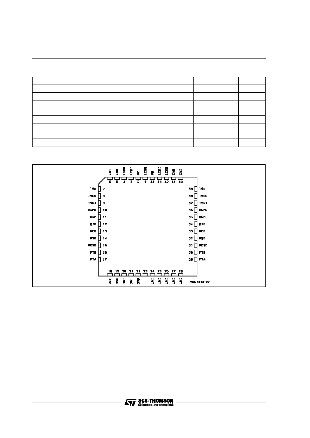
PIN CONNECTION (top view)
LAI
L6515
2/13
Page 3

Pin Name Description
1 LCSG Load Current Decoder Sens Reference Ground
2V
Z
Zener Clamp
3,43 LCDI Load Current Decoder Input
4,42 LCDO Load Current Decoder Output
5,41 EAO Error AmplifierOutput for Current Mode PWM Modulator
6,40 EAI Error Amplifier Input for Current Mode PWM Modulator
7,39 TSO Tacho Signal Output
8,38 TSPO Tacho SignalProcessor Output
9,37 TSPI Tacho Signal Processor Input
10,36 PWMN Current Mode PWM Output Inverted
11,35 PWM Current Mode PWM Output non Inverted
12,34 DIO Direction Indicator Digital Open Collector Output. A Low Level is cw,
A High Level is ccw Operation ofthe Motor
13,33 PCO Position Counter Digital Open Collector Output
14,32 PSO Phase Selector Output for Signal Differentation
15,31 POSO Positioning Output. The Output Becomes Activated via Position
Adress Decoder.
16,30 FTB Analog Input from PositionEncoder Phase B. Proposed Operation
Range is 2.8V + 1V.
17,29 FTA Analog Input from PositionEncoder Phase A. Proposed Operation
Range is 2.8V + 1V
18 REF Master Current Reference
19 OSC Oscillator
20,21 DAI Decoder Logic Input for Latch Select + Reset
22 GND Major and Logic Ground
23 to 28 LAI Latch Adress Input
44 V
S
Supply Voltage
PIN FUNCTIONS
L6515
3/13
Page 4
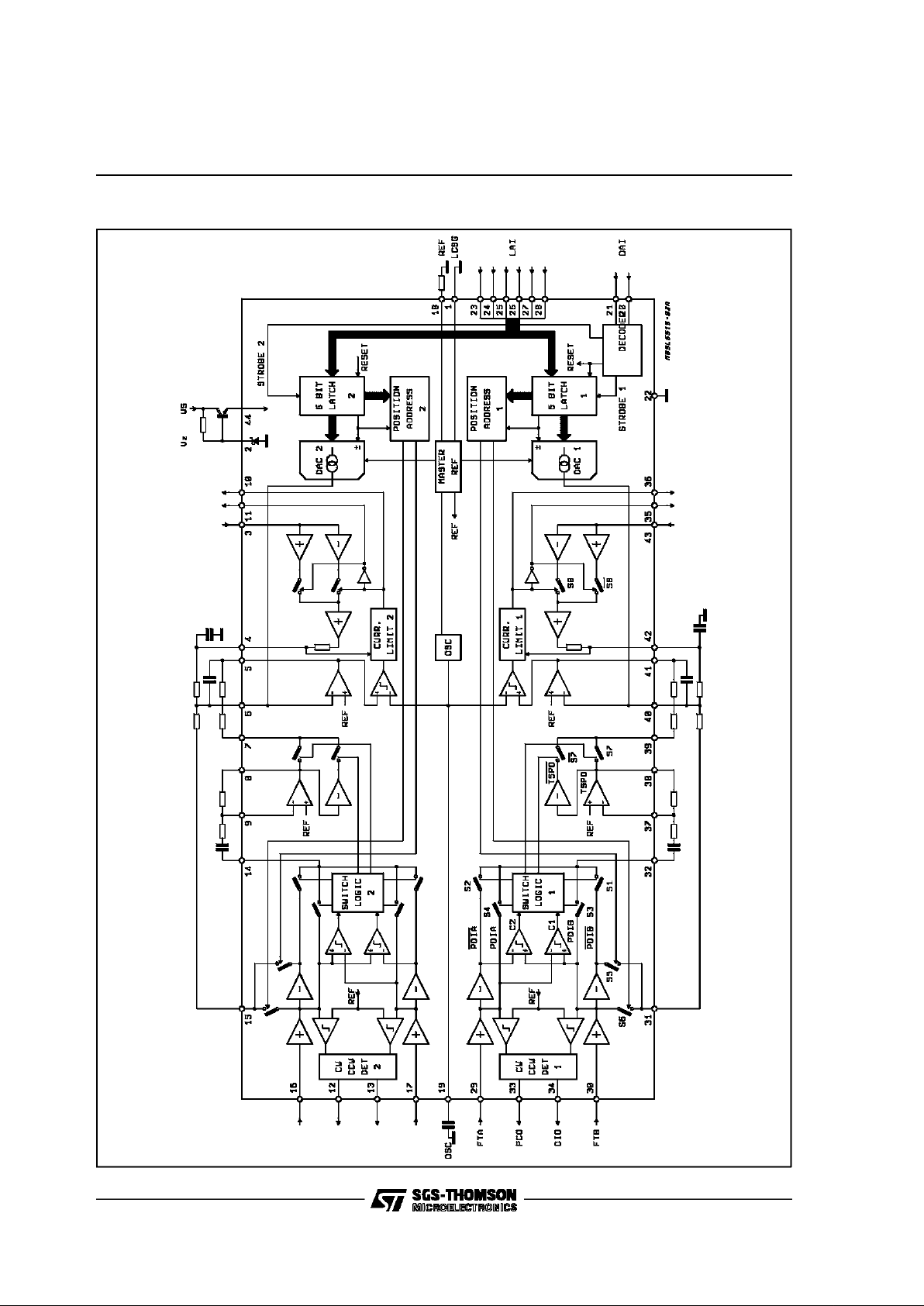
SCHEMATICDIAGRAM
L6515
4/13
Page 5

APPLICATIONCIRCUIT
L6515
5/13
Page 6

Symbol Parameter Pin Test Condition Min. Typ. Max. Unit
V
S
Operating Supply VoltageRange 7 11 V
I
S
Quiescent supply current 50 mA
V
Z
Zener Voltage Iz=1mA 8,5 9.9 11,4 V
I
Z
Operating Zener Current 1 mA
ELECTRICAL CHARACTERISTICS (refer to test circuit, VS=10V, I
REF
=300µA, T
amb
=25 °C unless
otherwisespecified)
V
I
Operating Input Voltage Range A/D/1/2 referredto V
REF
-1,65 +1,65 V
I
I
Input Bias Current 1 µA
V
OS
INput-output Offset Voltage Between
A/D/1/2 and F/1/2
S3 or S4
closed
I
o
=0
±15 mV
S1 or S2
closed
I
o
=0
V
IN=VREF
±20 mV
V
SAT
Output Saturation Voltage B/C/1/2 Io=1.4mA 0.4 V
I
OH
Output Leakage Current 10 µA
V
TH
ThresholdHysteresis
voltageBetween
A/1/2 and B/1/2
D/1/2 and C/1/2
80 150 mV
R
ON
Output Resistance ON State E/F/1/2 One of S1 to
S6 closed
150 300 Ω
V
OL
Output Operating Low Voltage E/F/1/2 referred
to V
REF
IO=1mA
-1.2 V
V
OH
OutpUt Operating High Voltage +1.2 V
POSITIONENCODER SECTION
L6515
6/13
Page 7

Symbol Parameter Pin Test Condition Min. Typ. Max. Unit
V
I
Input Voltage G/1/2 gain=1
referred
to V
REF
-1.65 +1.65 V
I
I
Input Bias Current 1 µA
V
OL
Output Operating Low Voltage H/1/2 referred to V
REF
-1.62
V
I/1/2
Io=1mAS7closed
-1.3
V
OH
Output Operating
low Voltage
I/1/2 +1.3
H/1/2 +1.62
R
ON
Output Resistance
On State
I1/2 S7 or S7
closed
150 260 Ω
V
OS
Input Offset Voltage H1/2 VIN=V
REF
S7 closed
I
o
=0
±20 mV
V
OS
Input Offset Voltage G1/2 referred to V
REF
g1/2 shorted
to H1/2
±20 mV
R
MO
Output Matching
Resistance
I1/2 S7 or S7
closed
0.8 1.2 Ω
TACHOSIGNALPROCESSINGSECTION
V
I
Input Voltage J1/2 gain=1 1 4.6 V
I
I
Input Bias Current 1 µA
V
O
L Lower Clamping Voltage K1/2 Io=1ma
refered to V
REF
-1.45 -1.22 V
V
OH
Higher Clamping Voltage +1.06 +1.56 V
V
OS
Input Offset Voltage J1/2 referred to V
REF
K1/2 J1/2 shorted
±20 mV
ERRORAMPLIFIERSECTION
V
OS
Output Offset Voltage L1/2 N1/2=0
referred to V
REF
±140 mV
R
OUT
Output Resistance 0.5 1.7 KΩ
V
CLH
Current Limit Threshold O1/2
P1/2
referred to V
REF
±0.5 V
V
CDO
Differential Output Offset Voltage L1/2 V
off(+)-Voff(-)
±20 mV
CURRENT DECODERSECTION
L6515
7/13
Page 8

Symbol Parameter Pin Test Condition Min. Typ. Max. Unit
V
H
Upper Triangle Threshold Referred to V
REF
+1.2 +1.8 V
V
L
Lower Triangle Threshold -1.6 -1.3 V
I
CD
Charge/Discharge Current I
REF
=500µA ±160 ±180 µA
V
O
PWM Output Voltage O1/2 Io=1.4mA 0.4 V
P1/2 2.7
OSCILLATOR-PWM SECTIONS
I
REF
Current Reference Input Range Z 0.3 0.7 mA
I
O
Sink and Source Output Current J1/2 I
REF
=0.5 mA 918 968 1018 µA
V
REF
Reference Voltage Z I
REF
=20 µa 2.7 2.8 2.9 V
I
O
LinearityError J1/2 I
REF
=0.5 mA 1.61 /FS
DACSECTION
V
INL
Input lOw Voltage R
S
-0.3 0.8 V
V
INH
Input High Voltage T
U
27V
I
L
Input V
W
-10 µA
I
H
Input High Current High Voltage X
Y
30 µA
INPUTLOGIC SECTION
L6515
8/13
Page 9

TRUTH TABLETACHO-ENCODER LOGIC
PDIB > PDIA C 1 = HIGH
PDIB < PDIA C 1 = LOW
PDIB > PDIA C2 = HIGH
PDIB < PDIA C2 = LOW
INPUTSIGNAL
C1 C2 CLOSED S2 POSITION
L H S1 TSPO
H H S2 TSPO
H L S3 TSPO
L L S4 TSPO
SWITCHSIGNAL
APPLICATIONCIRCUIT
L6515
9/13
Page 10

TRUTH TABLELOGICSELECTION CHIP ADDRESS
Terminals
Functions
RS
L L NO ACTION
H L STROBE LATCH 1
L H STROBE LATCH 2
H H RESET LATCH 1/2
DECODER ADDRESS
LATCH ADDRESS
TIMING DIAGRAM OF COUNTER AND DIRECTIONINDICATION LOGIC
L6515
10/13
Page 11

POSITIONENCODER
Main advantage of the operation principle of the
positioningsystem is that a high performancepositionencoder is not required.
The system accepts several phases and amplitude errors of the encoder output signal without
affectingthe systemperformance.
Two positionsensorsare useful.
1) Optical-Encoderwith IR-LED and Phototransistor
2) Magnetic Encoder with hall-effect sensors
The allowedspreadof theencoderoutput signal refer to referencelevel is shown in Fig.3.
Figure3.
Figure2.
Figure1.
L6515
11/13
Page 12

PLCC44PACKAGE MECHANICAL DATA
DIM.
mm inch
MIN. TYP. MAX. MIN. TYP. MAX.
A 17.4 17.65 0.685 0.695
B 16.51 16.65 0.650 0.656
C 3.65 3.7 0.144 0.146
D 4.2 4.57 0.165 0.180
d1 2.59 2.74 0.102 0.108
d2 0.68 0.027
E 14.99 16 0.590 0.630
e 1.27 0.050
e3 12.7 0.500
F 0.46 0.018
F1 0.71 0.028
G 0.101 0.004
M 1.16 0.046
M1 1.14 0.045
L6515
12/13
Page 13

Information furnished is believed to be accurate and reliable. However, SGS-THOMSON Microelectronics assumes no responsibility for the
consequences of use of such information nor for any infringement ofpatents or other rights of third parties whichmay result from itsuse. No
license is granted by implication or otherwise under any patent or patent rights of SGS-THOMSON Microelectronics. Specifications mentioned in this publication are subject to change without notice. This publication supersedes and replaces all information previously supplied.
SGS-THOMSON Microelectronics products are not authorized for use as critical components in life support devices or systems without express writtenapproval of SGS-THOMSON Microelectronics.
1994 SGS-THOMSON Microelectronics - All RightsReserved
SGS-THOMSON Microelectronics GROUP OF COMPANIES
Australia - Brazil- France -Germany - Hong Kong -Italy - Japan - Korea -Malaysia - Malta - Morocco -The Netherlands- Singapore -
Spain - Sweden - Switzerland- Taiwan - Thaliand - United Kingdom- U.S.A.
L6515
13/13
 Loading...