

Page 1
dSPIN fully integrated microstepping motor driver
Features
■ Operating voltage: 8 - 45 V
■ 7.0 A output peak current (3.0 A r.m.s.)
■ Low R
■ Programmable speed profile
■ Programmable Power MOSFET slew rate
■ Up to 1/16 microstepping
■ Predictive current control with adaptive decay
■ Non-dissipative current sensing
■ SPI interface
■ Low quiescent and standby currents
■ Programmable non-dissipative overcurrent
protection on all Power MOSFETs
■ Two levels of overtemperature protection
Applications
■ Bipolar stepper motor
power MOSFETs
DSon
L6472
with motion engine and SPI
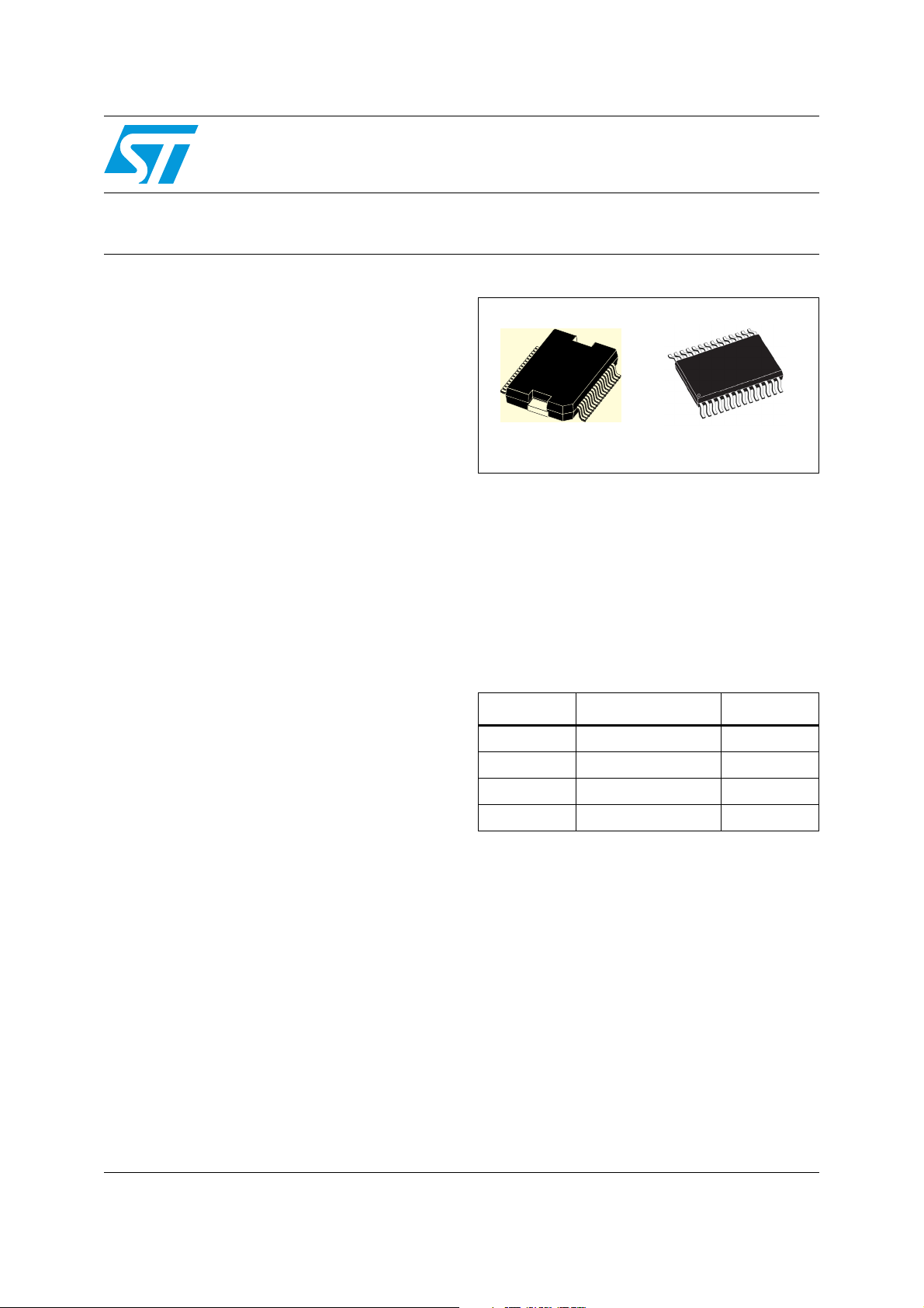
POWERSO36
All application commands and data registers,
including those used to set analog values (i.e.
current control value, current protection trip point,
dead time, etc.) are sent through a standard 5Mbit/s SPI.
A very rich set of protections (thermal, low bus
voltage, overcurrent) makes the L6472 “bullet
proof”, as required by the most demanding motor
control applications.
Table 1. Device summary
Order codes Package Packing
HTSSOP28
Description
L6472H HTSSOP28 Tube
L6472HTR HTSSOP28 Tape and reel
The L6472, realized in analog mixed signal
technology, is an advanced fully integrated
solution suitable for driving two-phase bipolar
stepper motors with microstepping. It integrates a
dual low R
DMOS full bridge with all of the
DS(on)
power switches equipped with an accurate onchip current sensing circuitry suitable for nondissipative current control and overcurrent
protection. Thanks to a new current control, a
1/16 microstepping is achieved through an
adaptive decay mode which outperforms
traditional implementations. The digital control
core can generate user defined motion profiles
with acceleration, deceleration, speed or target
position, easily programmed through a dedicated
register set.
January 2012 Doc ID 022729 Rev 1 1/69
L6472PD POWERSO36 Tube
L6472PDTR POWERSO36 Tape and reel
www.st.com
69
Page 2

Contents L6472
Contents
1 Block diagram . . . . . . . . . . . . . . . . . . . . . . . . . . . . . . . . . . . . . . . . . . . . . . 6
2 Electrical data . . . . . . . . . . . . . . . . . . . . . . . . . . . . . . . . . . . . . . . . . . . . . . 7
2.1 Absolute maximum ratings . . . . . . . . . . . . . . . . . . . . . . . . . . . . . . . . . . . . . 7
2.2 Recommended operating conditions . . . . . . . . . . . . . . . . . . . . . . . . . . . . . 8
2.3 Thermal data . . . . . . . . . . . . . . . . . . . . . . . . . . . . . . . . . . . . . . . . . . . . . . . 8
3 Electrical characteristics . . . . . . . . . . . . . . . . . . . . . . . . . . . . . . . . . . . . . 9
4 Pin connection . . . . . . . . . . . . . . . . . . . . . . . . . . . . . . . . . . . . . . . . . . . . . 14
4.1 Pin list . . . . . . . . . . . . . . . . . . . . . . . . . . . . . . . . . . . . . . . . . . . . . . . . . . . . 15
5 Typical applications . . . . . . . . . . . . . . . . . . . . . . . . . . . . . . . . . . . . . . . . 17
6 Functional description . . . . . . . . . . . . . . . . . . . . . . . . . . . . . . . . . . . . . . 18
6.1 Device power-up . . . . . . . . . . . . . . . . . . . . . . . . . . . . . . . . . . . . . . . . . . . . 18
6.2 Logic I/O . . . . . . . . . . . . . . . . . . . . . . . . . . . . . . . . . . . . . . . . . . . . . . . . . . 18
6.3 Charge pump . . . . . . . . . . . . . . . . . . . . . . . . . . . . . . . . . . . . . . . . . . . . . . 18
6.4 Microstepping . . . . . . . . . . . . . . . . . . . . . . . . . . . . . . . . . . . . . . . . . . . . . . 19
6.4.1 Automatic full-step mode . . . . . . . . . . . . . . . . . . . . . . . . . . . . . . . . . . . . 20
6.5 Absolute position counter . . . . . . . . . . . . . . . . . . . . . . . . . . . . . . . . . . . . . 20
6.6 Programmable speed profiles . . . . . . . . . . . . . . . . . . . . . . . . . . . . . . . . . 20
6.6.1 Infinite acceleration/deceleration mode . . . . . . . . . . . . . . . . . . . . . . . . . 21
6.7 Motor control commands . . . . . . . . . . . . . . . . . . . . . . . . . . . . . . . . . . . . . 21
6.7.1 Constant speed commands . . . . . . . . . . . . . . . . . . . . . . . . . . . . . . . . . . 21
6.7.2 Positioning commands . . . . . . . . . . . . . . . . . . . . . . . . . . . . . . . . . . . . . . 22
6.7.3 Motion commands . . . . . . . . . . . . . . . . . . . . . . . . . . . . . . . . . . . . . . . . . 23
6.7.4 Stop commands . . . . . . . . . . . . . . . . . . . . . . . . . . . . . . . . . . . . . . . . . . . 23
6.7.5 Step-clock mode . . . . . . . . . . . . . . . . . . . . . . . . . . . . . . . . . . . . . . . . . . 23
6.7.6 GoUntil and ReleaseSW commands . . . . . . . . . . . . . . . . . . . . . . . . . . . 24
6.8 Internal oscillator and oscillator driver . . . . . . . . . . . . . . . . . . . . . . . . . . . 25
6.8.1 Internal oscillator . . . . . . . . . . . . . . . . . . . . . . . . . . . . . . . . . . . . . . . . . . 25
6.8.2 External clock source . . . . . . . . . . . . . . . . . . . . . . . . . . . . . . . . . . . . . . . 25
2/69 Doc ID 022729 Rev 1
Page 3

L6472 Contents
6.9 Overcurrent detection . . . . . . . . . . . . . . . . . . . . . . . . . . . . . . . . . . . . . . . . 26
6.10 Undervoltage lockout (UVLO) . . . . . . . . . . . . . . . . . . . . . . . . . . . . . . . . . 27
6.11 Thermal warning and thermal shutdown . . . . . . . . . . . . . . . . . . . . . . . . . 27
6.12 Reset and standby . . . . . . . . . . . . . . . . . . . . . . . . . . . . . . . . . . . . . . . . . . 27
6.13 External switch (SW pin) . . . . . . . . . . . . . . . . . . . . . . . . . . . . . . . . . . . . . 28
6.14 Programmable DMOS slew rate, dead time and blanking time . . . . . . . . 28
6.15 Integrated analog-to-digital converter . . . . . . . . . . . . . . . . . . . . . . . . . . . . 28
6.16 Internal voltage regulator . . . . . . . . . . . . . . . . . . . . . . . . . . . . . . . . . . . . . 29
6.17 BUSY\SYNC pin . . . . . . . . . . . . . . . . . . . . . . . . . . . . . . . . . . . . . . . . . . . . 29
6.17.1 BUSY operation mode . . . . . . . . . . . . . . . . . . . . . . . . . . . . . . . . . . . . . . 29
6.17.2 SYNC operation mode . . . . . . . . . . . . . . . . . . . . . . . . . . . . . . . . . . . . . . 30
6.18 FLAG pin . . . . . . . . . . . . . . . . . . . . . . . . . . . . . . . . . . . . . . . . . . . . . . . . . 30
7 Phase current control . . . . . . . . . . . . . . . . . . . . . . . . . . . . . . . . . . . . . . . 31
7.1 Predictive current control . . . . . . . . . . . . . . . . . . . . . . . . . . . . . . . . . . . . . 31
7.2 Auto-adjusted decay mode . . . . . . . . . . . . . . . . . . . . . . . . . . . . . . . . . . . . 33
7.3 Auto-adjusted fast decay during the falling steps . . . . . . . . . . . . . . . . . . . 34
7.4 Torque regulation (output current amplitude regulation) . . . . . . . . . . . . . . 35
8 Serial interface . . . . . . . . . . . . . . . . . . . . . . . . . . . . . . . . . . . . . . . . . . . . . 36
9 Programming manual . . . . . . . . . . . . . . . . . . . . . . . . . . . . . . . . . . . . . . . 38
9.1 Register and flag description . . . . . . . . . . . . . . . . . . . . . . . . . . . . . . . . . . 38
9.1.1 ABS_POS . . . . . . . . . . . . . . . . . . . . . . . . . . . . . . . . . . . . . . . . . . . . . . . 39
9.1.2 EL_POS . . . . . . . . . . . . . . . . . . . . . . . . . . . . . . . . . . . . . . . . . . . . . . . . . 39
9.1.3 MARK . . . . . . . . . . . . . . . . . . . . . . . . . . . . . . . . . . . . . . . . . . . . . . . . . . 40
9.1.4 SPEED . . . . . . . . . . . . . . . . . . . . . . . . . . . . . . . . . . . . . . . . . . . . . . . . . . 40
9.1.5 ACC . . . . . . . . . . . . . . . . . . . . . . . . . . . . . . . . . . . . . . . . . . . . . . . . . . . . 40
9.1.6 DEC . . . . . . . . . . . . . . . . . . . . . . . . . . . . . . . . . . . . . . . . . . . . . . . . . . . . 40
9.1.7 MAX_SPEED . . . . . . . . . . . . . . . . . . . . . . . . . . . . . . . . . . . . . . . . . . . . . 41
9.1.8 MIN_SPEED . . . . . . . . . . . . . . . . . . . . . . . . . . . . . . . . . . . . . . . . . . . . . 41
9.1.9 FS_SPD . . . . . . . . . . . . . . . . . . . . . . . . . . . . . . . . . . . . . . . . . . . . . . . . . 42
9.1.10 TVAL_HOLD, TVAL_RUN, TVAL_ACC and TVAL_DEC . . . . . . . . . . . . 42
9.1.11 T_FAST . . . . . . . . . . . . . . . . . . . . . . . . . . . . . . . . . . . . . . . . . . . . . . . . . 43
9.1.12 TON_MIN . . . . . . . . . . . . . . . . . . . . . . . . . . . . . . . . . . . . . . . . . . . . . . . . 43
9.1.13 TOFF_MIN . . . . . . . . . . . . . . . . . . . . . . . . . . . . . . . . . . . . . . . . . . . . . . . 44
Doc ID 022729 Rev 1 3/69
Page 4

Contents L6472
9.1.14 ADC_OUT . . . . . . . . . . . . . . . . . . . . . . . . . . . . . . . . . . . . . . . . . . . . . . . 45
9.1.15 OCD_TH . . . . . . . . . . . . . . . . . . . . . . . . . . . . . . . . . . . . . . . . . . . . . . . . 45
9.1.16 STEP_MODE . . . . . . . . . . . . . . . . . . . . . . . . . . . . . . . . . . . . . . . . . . . . . 46
9.1.17 ALARM_EN . . . . . . . . . . . . . . . . . . . . . . . . . . . . . . . . . . . . . . . . . . . . . . 48
9.1.18 CONFIG . . . . . . . . . . . . . . . . . . . . . . . . . . . . . . . . . . . . . . . . . . . . . . . . . 48
9.1.19 STATUS . . . . . . . . . . . . . . . . . . . . . . . . . . . . . . . . . . . . . . . . . . . . . . . . . 51
9.2 Application commands . . . . . . . . . . . . . . . . . . . . . . . . . . . . . . . . . . . . . . . 52
9.2.1 Command management . . . . . . . . . . . . . . . . . . . . . . . . . . . . . . . . . . . . 53
9.2.2 Nop . . . . . . . . . . . . . . . . . . . . . . . . . . . . . . . . . . . . . . . . . . . . . . . . . . . . 53
9.2.3 SetParam (PARAM, VALUE) . . . . . . . . . . . . . . . . . . . . . . . . . . . . . . . . . 54
9.2.4 GetParam (PARAM) . . . . . . . . . . . . . . . . . . . . . . . . . . . . . . . . . . . . . . . . 54
9.2.5 Run (DIR, SPD) . . . . . . . . . . . . . . . . . . . . . . . . . . . . . . . . . . . . . . . . . . . 55
9.2.6 StepClock (DIR) . . . . . . . . . . . . . . . . . . . . . . . . . . . . . . . . . . . . . . . . . . . 55
9.2.7 Move (DIR, N_STEP) . . . . . . . . . . . . . . . . . . . . . . . . . . . . . . . . . . . . . . . 56
9.2.8 GoTo (ABS_POS) . . . . . . . . . . . . . . . . . . . . . . . . . . . . . . . . . . . . . . . . . 56
9.2.9 GoTo_DIR (DIR, ABS_POS) . . . . . . . . . . . . . . . . . . . . . . . . . . . . . . . . . 57
9.2.10 GoUntil (ACT, DIR, SPD) . . . . . . . . . . . . . . . . . . . . . . . . . . . . . . . . . . . . 57
9.2.11 ReleaseSW (ACT, DIR) . . . . . . . . . . . . . . . . . . . . . . . . . . . . . . . . . . . . . 58
9.2.12 GoHome . . . . . . . . . . . . . . . . . . . . . . . . . . . . . . . . . . . . . . . . . . . . . . . . 58
9.2.13 GoMark . . . . . . . . . . . . . . . . . . . . . . . . . . . . . . . . . . . . . . . . . . . . . . . . . 58
9.2.14 ResetPos . . . . . . . . . . . . . . . . . . . . . . . . . . . . . . . . . . . . . . . . . . . . . . . . 59
9.2.15 ResetDevice . . . . . . . . . . . . . . . . . . . . . . . . . . . . . . . . . . . . . . . . . . . . . . 59
9.2.16 SoftStop . . . . . . . . . . . . . . . . . . . . . . . . . . . . . . . . . . . . . . . . . . . . . . . . . 59
9.2.17 HardStop . . . . . . . . . . . . . . . . . . . . . . . . . . . . . . . . . . . . . . . . . . . . . . . . 60
9.2.18 SoftHiZ . . . . . . . . . . . . . . . . . . . . . . . . . . . . . . . . . . . . . . . . . . . . . . . . . . 60
9.2.19 HardHiZ . . . . . . . . . . . . . . . . . . . . . . . . . . . . . . . . . . . . . . . . . . . . . . . . . 60
9.2.20 GetStatus . . . . . . . . . . . . . . . . . . . . . . . . . . . . . . . . . . . . . . . . . . . . . . . . 61
10 Package mechanical data . . . . . . . . . . . . . . . . . . . . . . . . . . . . . . . . . . . . 62
11 Revision history . . . . . . . . . . . . . . . . . . . . . . . . . . . . . . . . . . . . . . . . . . . 66
4/69 Doc ID 022729 Rev 1
Page 5

L6472 List of tables
List of tables
Table 1. Device summary . . . . . . . . . . . . . . . . . . . . . . . . . . . . . . . . . . . . . . . . . . . . . . . . . . . . . . . . . . 1
Table 2. Absolute maximum ratings . . . . . . . . . . . . . . . . . . . . . . . . . . . . . . . . . . . . . . . . . . . . . . . . . . 8
Table 3. Recommended operating conditions . . . . . . . . . . . . . . . . . . . . . . . . . . . . . . . . . . . . . . . . . . 9
Table 4. Thermal data. . . . . . . . . . . . . . . . . . . . . . . . . . . . . . . . . . . . . . . . . . . . . . . . . . . . . . . . . . . . . 9
Table 5. Electrical characteristics . . . . . . . . . . . . . . . . . . . . . . . . . . . . . . . . . . . . . . . . . . . . . . . . . . . 10
Table 6. Pin description . . . . . . . . . . . . . . . . . . . . . . . . . . . . . . . . . . . . . . . . . . . . . . . . . . . . . . . . . . 16
Table 7. Typical application values . . . . . . . . . . . . . . . . . . . . . . . . . . . . . . . . . . . . . . . . . . . . . . . . . . 18
Table 8. CL values according to external oscillator frequency . . . . . . . . . . . . . . . . . . . . . . . . . . . . . 26
Table 9. Register map . . . . . . . . . . . . . . . . . . . . . . . . . . . . . . . . . . . . . . . . . . . . . . . . . . . . . . . . . . . 39
Table 10. EL_POS register . . . . . . . . . . . . . . . . . . . . . . . . . . . . . . . . . . . . . . . . . . . . . . . . . . . . . . . . . 40
Table 11. MIN_SPEED register . . . . . . . . . . . . . . . . . . . . . . . . . . . . . . . . . . . . . . . . . . . . . . . . . . . . . 42
Table 12. Torque regulation by TVAL_HOLD, TVAL_ACC, TVAL_DEC and TVAL_RUN registers . 43
Table 13. Maximum fast decay times . . . . . . . . . . . . . . . . . . . . . . . . . . . . . . . . . . . . . . . . . . . . . . . . . 44
Table 14. Minimum ON time . . . . . . . . . . . . . . . . . . . . . . . . . . . . . . . . . . . . . . . . . . . . . . . . . . . . . . . . 44
Table 15. Minimum OFF time . . . . . . . . . . . . . . . . . . . . . . . . . . . . . . . . . . . . . . . . . . . . . . . . . . . . . . . 45
Table 16. ADC_OUT value and torque regulation feature . . . . . . . . . . . . . . . . . . . . . . . . . . . . . . . . . 46
Table 17. Overcurrent detection threshold . . . . . . . . . . . . . . . . . . . . . . . . . . . . . . . . . . . . . . . . . . . . . 46
Table 18. STEP_MODE register. . . . . . . . . . . . . . . . . . . . . . . . . . . . . . . . . . . . . . . . . . . . . . . . . . . . . 47
Table 19. Step mode selection . . . . . . . . . . . . . . . . . . . . . . . . . . . . . . . . . . . . . . . . . . . . . . . . . . . . . . 47
Table 20. SYNC output frequency . . . . . . . . . . . . . . . . . . . . . . . . . . . . . . . . . . . . . . . . . . . . . . . . . . . 48
Table 21. SYNC signal source . . . . . . . . . . . . . . . . . . . . . . . . . . . . . . . . . . . . . . . . . . . . . . . . . . . . . . 48
Table 22. ALARM_EN register . . . . . . . . . . . . . . . . . . . . . . . . . . . . . . . . . . . . . . . . . . . . . . . . . . . . . . 49
Table 23. CONFIG register . . . . . . . . . . . . . . . . . . . . . . . . . . . . . . . . . . . . . . . . . . . . . . . . . . . . . . . . . 49
Table 24. Oscillator management. . . . . . . . . . . . . . . . . . . . . . . . . . . . . . . . . . . . . . . . . . . . . . . . . . . . 50
Table 25. External switch hard stop interrupt mode . . . . . . . . . . . . . . . . . . . . . . . . . . . . . . . . . . . . . . 50
Table 26. Overcurrent event . . . . . . . . . . . . . . . . . . . . . . . . . . . . . . . . . . . . . . . . . . . . . . . . . . . . . . . . 51
Table 27. Programmable power bridge output slew rate values. . . . . . . . . . . . . . . . . . . . . . . . . . . . . 51
Table 28. External torque regulation enable . . . . . . . . . . . . . . . . . . . . . . . . . . . . . . . . . . . . . . . . . . . . 51
Table 29. Switching period . . . . . . . . . . . . . . . . . . . . . . . . . . . . . . . . . . . . . . . . . . . . . . . . . . . . . . . . . 51
Table 30. STATUS register. . . . . . . . . . . . . . . . . . . . . . . . . . . . . . . . . . . . . . . . . . . . . . . . . . . . . . . . . 52
Table 31. STATUS register DIR bit. . . . . . . . . . . . . . . . . . . . . . . . . . . . . . . . . . . . . . . . . . . . . . . . . . . 52
Table 32. STATUS register MOT_STATE bits . . . . . . . . . . . . . . . . . . . . . . . . . . . . . . . . . . . . . . . . . . 52
Table 33. Application commands . . . . . . . . . . . . . . . . . . . . . . . . . . . . . . . . . . . . . . . . . . . . . . . . . . . . 53
Table 34. NOP command structure . . . . . . . . . . . . . . . . . . . . . . . . . . . . . . . . . . . . . . . . . . . . . . . . . . 54
Table 35. SetParam command structure . . . . . . . . . . . . . . . . . . . . . . . . . . . . . . . . . . . . . . . . . . . . . . 55
Table 36. GetParam command structure . . . . . . . . . . . . . . . . . . . . . . . . . . . . . . . . . . . . . . . . . . . . . . 55
Table 37. Run command structure . . . . . . . . . . . . . . . . . . . . . . . . . . . . . . . . . . . . . . . . . . . . . . . . . . . 56
Table 38. StepClock command structure . . . . . . . . . . . . . . . . . . . . . . . . . . . . . . . . . . . . . . . . . . . . . . 56
Table 39. Move command structure . . . . . . . . . . . . . . . . . . . . . . . . . . . . . . . . . . . . . . . . . . . . . . . . . . 57
Table 40. GoTo command structure . . . . . . . . . . . . . . . . . . . . . . . . . . . . . . . . . . . . . . . . . . . . . . . . . . 57
Table 41. GoTo_DIR command structure. . . . . . . . . . . . . . . . . . . . . . . . . . . . . . . . . . . . . . . . . . . . . . 58
Table 42. GoUntil command structure . . . . . . . . . . . . . . . . . . . . . . . . . . . . . . . . . . . . . . . . . . . . . . . . 58
Table 43. ReleaseSW command structure . . . . . . . . . . . . . . . . . . . . . . . . . . . . . . . . . . . . . . . . . . . . . 59
Table 44. GoHome command structure . . . . . . . . . . . . . . . . . . . . . . . . . . . . . . . . . . . . . . . . . . . . . . . 59
Table 45. ResetPos command structure . . . . . . . . . . . . . . . . . . . . . . . . . . . . . . . . . . . . . . . . . . . . . . 60
Table 46. ResetDevice command structure. . . . . . . . . . . . . . . . . . . . . . . . . . . . . . . . . . . . . . . . . . . . 60
Table 47. SoftStop command structure . . . . . . . . . . . . . . . . . . . . . . . . . . . . . . . . . . . . . . . . . . . . . . . 60
Table 48. HardStop command structure . . . . . . . . . . . . . . . . . . . . . . . . . . . . . . . . . . . . . . . . . . . . . . 61
Doc ID 022729 Rev 1 5/69
Page 6

List of tables L6472
Table 49. SoftHiZ command structure . . . . . . . . . . . . . . . . . . . . . . . . . . . . . . . . . . . . . . . . . . . . . . . . 61
Table 50. HardHiZ command structure. . . . . . . . . . . . . . . . . . . . . . . . . . . . . . . . . . . . . . . . . . . . . . . . 61
Table 51. GetStatus command structure . . . . . . . . . . . . . . . . . . . . . . . . . . . . . . . . . . . . . . . . . . . . . . 62
Table 52. HTSSOP28 mechanical data . . . . . . . . . . . . . . . . . . . . . . . . . . . . . . . . . . . . . . . . . . . . . . . 63
Table 53. POWERSO36 mechanical data . . . . . . . . . . . . . . . . . . . . . . . . . . . . . . . . . . . . . . . . . . . . . 65
Table 54. Document revision history . . . . . . . . . . . . . . . . . . . . . . . . . . . . . . . . . . . . . . . . . . . . . . . . . 67
6/69 Doc ID 022729 Rev 1
Page 7

L6472 List of figures
List of figures
Figure 1. Block diagram . . . . . . . . . . . . . . . . . . . . . . . . . . . . . . . . . . . . . . . . . . . . . . . . . . . . . . . . . . . . 8
Figure 2. HTSSOP28 pin connection (top view) . . . . . . . . . . . . . . . . . . . . . . . . . . . . . . . . . . . . . . . . 16
Figure 3. POWERSO36 pin connection (top view) . . . . . . . . . . . . . . . . . . . . . . . . . . . . . . . . . . . . . . 16
Figure 4. Bipolar stepper motor control application using the L6472 . . . . . . . . . . . . . . . . . . . . . . . . . 19
Figure 5. Charge pump circuitry. . . . . . . . . . . . . . . . . . . . . . . . . . . . . . . . . . . . . . . . . . . . . . . . . . . . . 21
Figure 6. Normal mode and microstepping (16 microsteps) . . . . . . . . . . . . . . . . . . . . . . . . . . . . . . . 21
Figure 7. Automatic full-step switching . . . . . . . . . . . . . . . . . . . . . . . . . . . . . . . . . . . . . . . . . . . . . . . 22
Figure 8. Speed profile in infinite acceleration/deceleration mode . . . . . . . . . . . . . . . . . . . . . . . . . . 23
Figure 9. Constant speed commands examples . . . . . . . . . . . . . . . . . . . . . . . . . . . . . . . . . . . . . . . . 24
Figure 10. Positioning command examples . . . . . . . . . . . . . . . . . . . . . . . . . . . . . . . . . . . . . . . . . . . . . 24
Figure 11. Motion command examples . . . . . . . . . . . . . . . . . . . . . . . . . . . . . . . . . . . . . . . . . . . . . . . . 25
Figure 12. OSCIN and OSCOUT pin configurations . . . . . . . . . . . . . . . . . . . . . . . . . . . . . . . . . . . . . . 28
Figure 13. External switch connection . . . . . . . . . . . . . . . . . . . . . . . . . . . . . . . . . . . . . . . . . . . . . . . . . 30
Figure 14. Internal 3 V linear regulator . . . . . . . . . . . . . . . . . . . . . . . . . . . . . . . . . . . . . . . . . . . . . . . . 31
Figure 15. Predictive current control . . . . . . . . . . . . . . . . . . . . . . . . . . . . . . . . . . . . . . . . . . . . . . . . . . 33
Figure 16. Non-predictive current control. . . . . . . . . . . . . . . . . . . . . . . . . . . . . . . . . . . . . . . . . . . . . . . 34
Figure 17. Adaptive decay - fast decay tuning . . . . . . . . . . . . . . . . . . . . . . . . . . . . . . . . . . . . . . . . . . . 35
Figure 18. Adaptive decay - switch from normal to slow+fast decay mode and vice versa . . . . . . . . . 36
Figure 19. Fast decay tuning during the falling steps . . . . . . . . . . . . . . . . . . . . . . . . . . . . . . . . . . . . . 37
Figure 20. SPI timings diagram . . . . . . . . . . . . . . . . . . . . . . . . . . . . . . . . . . . . . . . . . . . . . . . . . . . . . . 38
Figure 21. Daisy chain configuration . . . . . . . . . . . . . . . . . . . . . . . . . . . . . . . . . . . . . . . . . . . . . . . . . . 39
Figure 22. Command with 3-byte argument. . . . . . . . . . . . . . . . . . . . . . . . . . . . . . . . . . . . . . . . . . . . . 55
Figure 23. Command with 3-byte response . . . . . . . . . . . . . . . . . . . . . . . . . . . . . . . . . . . . . . . . . . . . . 55
Figure 24. Command response aborted . . . . . . . . . . . . . . . . . . . . . . . . . . . . . . . . . . . . . . . . . . . . . . . 55
Figure 25. HTSSOP28 mechanical data . . . . . . . . . . . . . . . . . . . . . . . . . . . . . . . . . . . . . . . . . . . . . . . 65
Figure 26. POWERSO36 drawings . . . . . . . . . . . . . . . . . . . . . . . . . . . . . . . . . . . . . . . . . . . . . . . . . . . 67
Doc ID 022729 Rev 1 7/69
Page 8
Block diagram L6472
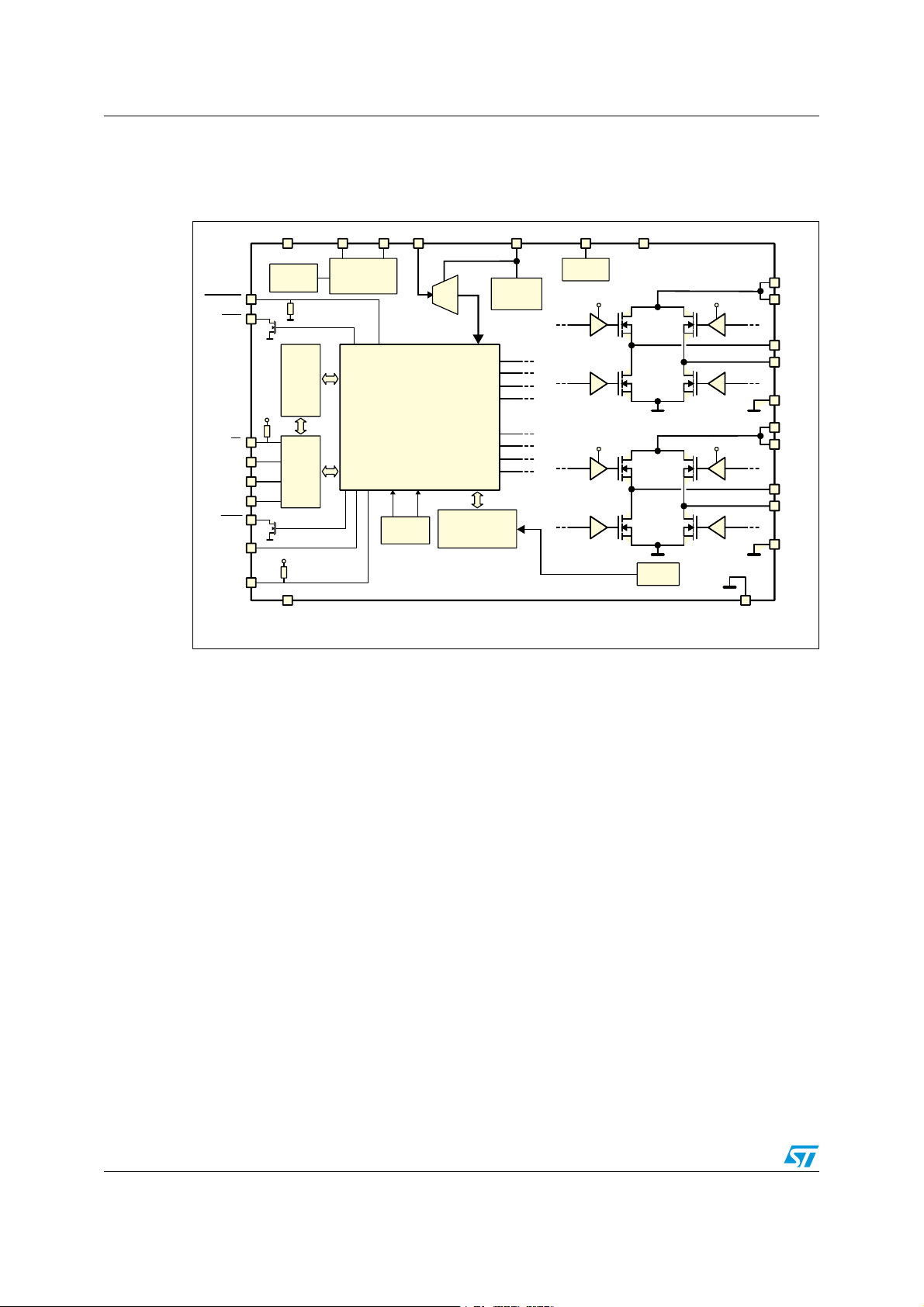
1 Block diagram
Figure 1. Block diagram
6$
$ /3#). /3 4//"60#'%26.)#$!45/#
34"9234
&,!'
3$/
3$)
"53939.#
34#+
37
(3
,3
(3
,3
#HARGE
PUMP
!
!
"
"
63!
6
BOOT
6
BOOT
#URRENT
SENSING
6
BOOT
(3
,3
6
BOOT
(3
,3
!'.$
63!
!
/54!
/54!
!
0'.$
63"
63"
"
/54"
/54"
"
0'.$
-(Z
/SCILLATOR
6
$$
#3
#+
%XT/SCDRIVER
2EGISTERS
#LOCKGEN
#ONTROL
,OGIC
!$#
6
6OLTAGE2EG
(3
!
,3
!
(3
!
,3
!
(3
"
,3
"
(3
"
,3
"
30)
#URRENT$!#S
#OMPARATORS
6
$$
$'.$
4EMPERATURE
SENSING
!-V
8/69 Doc ID 022729 Rev 1
Page 9
L6472 Electrical data
2 Electrical data
2.1 Absolute maximum ratings
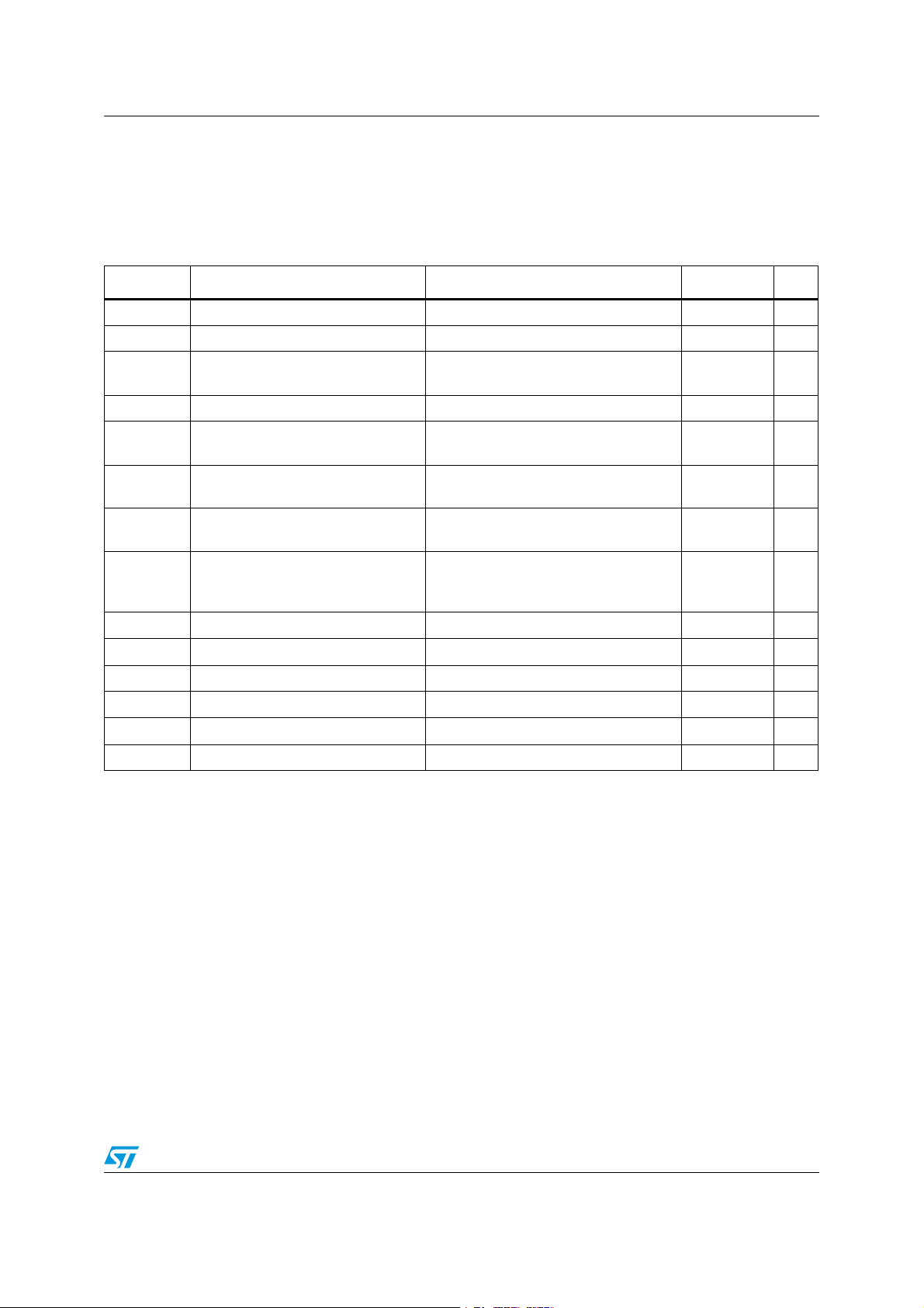
Table 2. Absolute maximum ratings
Symbol Parameter Test condition Value Unit
VDD Logic interface supply voltage 5.5 V
VS Motor supply voltage VSA = VSB = VS 48 V
Differential voltage between AGND,
V
V
V
V
I
out_peak
1. Maximum output current limit is related to metal connection and bonding characteristics. Actual limit must satisfy maximum
thermal dissipation constraints.
2. HTSSOP28 mounted on EVAL6472H Rev 1.0.
GND, diff
V
boot
V
REG
ADCIN
V
OSC
out_diff
LOGIC
I
out
T
OP
T
P
tot
PGND and DGND
Bootstrap peak voltage 55 V
Internal voltage regulator output pin
and logic supply voltage
Integrated ADC input voltage range
(ADCIN pin)
OSCIN and OSCOUT pin voltage
range
Differential voltage between V
, OUT2A, PGND and VSB,
OUT1
A
OUT1
, OUT2B, PGND pins
B
SA
,
= VSB = VS 48 V
V
SA
Logic inputs voltage range -0.3 to +5.5 V
(1)
R.m.s. output current 3 A
(1)
Pulsed output current T
< 1 ms 7 A
PULSE
Operating junction temperature 150 °C
Storage temperature range -55 to 150 °C
s
Total power dissipation (TA = 25 °C)
(2)
±0.3 V
3.6 V
-0.3 to +3.6 V
-0.3 to +3.6 V
5W
Doc ID 022729 Rev 1 9/69
Page 10
Electrical data L6472
2.2 Recommended operating conditions
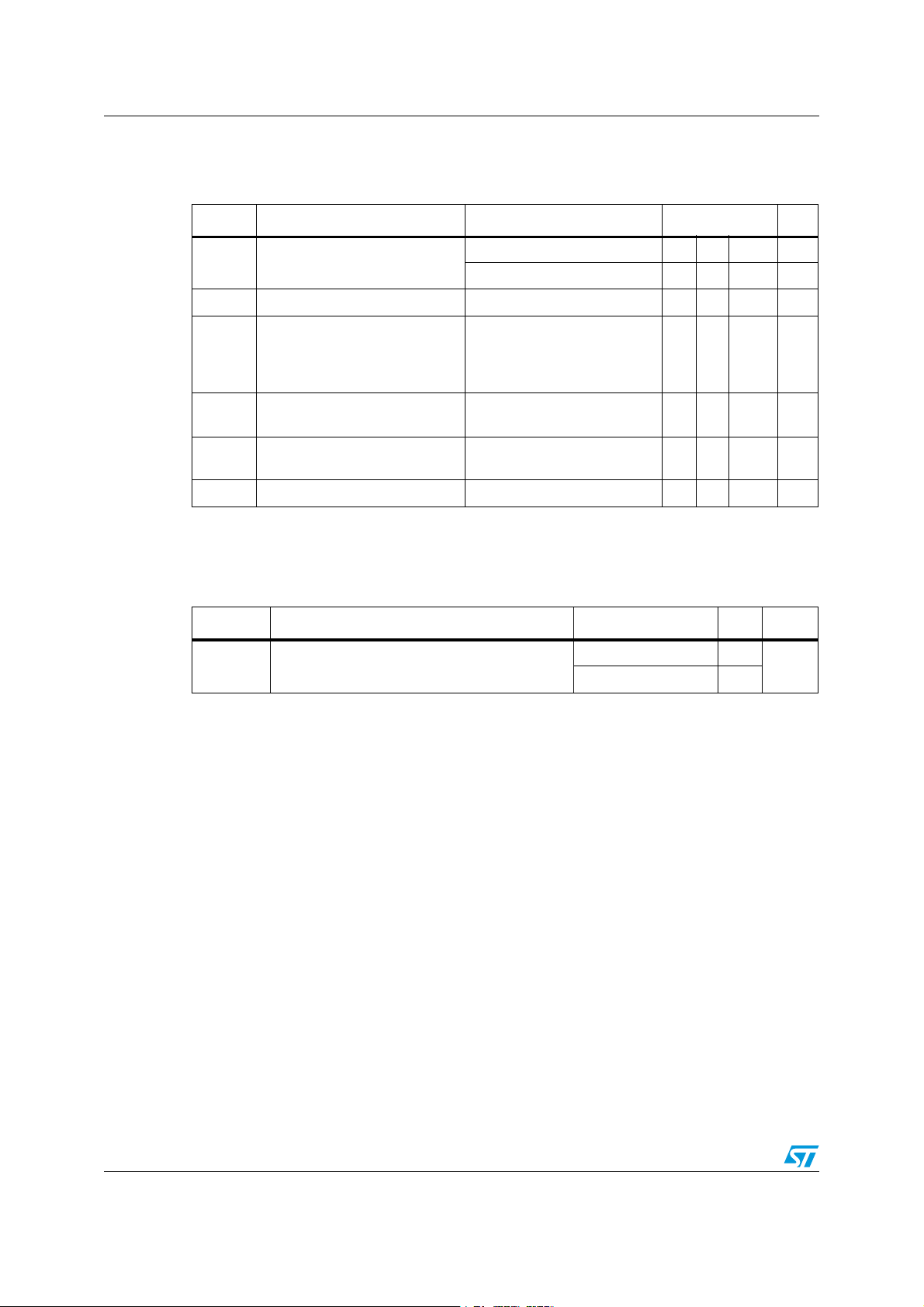
Table 3. Recommended operating conditions
Symbol Parameter Test condition Value Unit
V
Logic interface supply voltage
DD
V
Motor supply voltage VSA = VSB = VS 8 45 V
S
Differential voltage between
, OUT1A, OUT2A, PGND
V
V
out_diff
SA
and V
, OUT1B, OUT2B,
SB
PGND pins
V
Logic supply voltage
REG,in
Integrated ADC input voltage
V
ADC
(ADCIN pin)
Operating junction temperature -25 125 °C
T
j
2.3 Thermal data
Table 4. Thermal data
Symbol Parameter Package Typ Unit
R
thJA
1. HTSSOP28 mounted on EVAL6472H Rev 1.0 board: four-layer FR4 PCB with a dissipating copper surface
of about 40 cm
2. POWERSO36 mounted on EVAL6472PD Rev 1.0 board: four-layer FR4 PCB with a dissipating copper
surface of about 40 cm
Thermal resistance junction-ambient
2
on each layer and 15 via holes below the IC.
3.3 V logic outputs 3.3 V
5 V logic outputs 5
V
= V
= VS 45 V
SB
voltage imposed by
V
SA
REG
external source
2
on each layer and 22 via holes below the IC.
3.2 3.3 V
HTSSOP28
POWERSO36
0 V
(1)
(2)
22
12
REG
V
°C/W
10/69 Doc ID 022729 Rev 1
Page 11
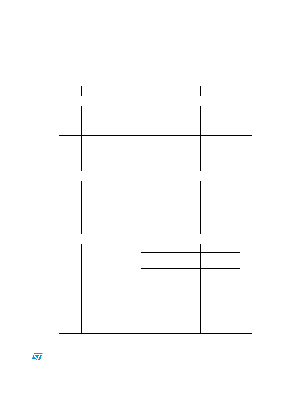
L6472 Electrical characteristics
3 Electrical characteristics
VSA = VSB = 36 V; VDD = 3.3 V; internal 3 V regulator; TJ = 25 °C, unless otherwise
specified.
Table 5. Electrical characteristics
Symbol Parameter Test condition Min. Typ. Max. Unit
General
V
SthOn VS
V
SthOff
V
SthHyst
Iq
T
j(WRN)
T
j(SD)
UVLO turn-on threshold 7.5 8.2 8.9 V
VS UVLO turn-off threshold 6.6 7.2 7.8 V
VS UVLO threshold
hysteresis
Quiescent motor supply
current
Thermal warning temperature 130 °C
Thermal shutdown
temperature
Charge pump
pump
f
pump,min
f
pump,max
I
boot
pump oscillator
Minimum charge pump
oscillator frequency
Maximum charge pump
oscillator frequency
Average boot current
Voltage swing for charge
V
Output DMOS transistor
High-side switch onresistance
R
DS(on)
Low-side switch onresistance
I
DSS
Leakage current
(1)
(1)
0.7 1 1.3 V
Internal oscillator selected;
= 3.3V ext; CP floating
V
REG
= f
f
sw,A
= 15.6kHz
sw,B
POW_SR = ‘10’
T
= 25°C, I
j
Tj = 125°C,
= 25°C, I
T
j
T
= 125°C,
j
OUT = V
= 3A 0.37
out
(2)
I
= 3A 0.51
out
= 3A 0.18
out
(2)
I
= 3A 0.23
out
S
OUT = GND -0.3
0.5 0.65 mA
160 °C
10 V
660 kHz
800 kHz
1.1 1.4 mA
Ω
3.1
mA
Rise time
t
r
(3)
POW_SR = '00', I
POW_SR = '00', I
POW_SR = ‘11’, I
POW_SR = ‘10’, I
POW_SR = ‘01’, I
= +1A 100
out
= -1A 80
out
= ±1A 100
out
= ±1A 200
out
= ±1A 300
out
ns
Doc ID 022729 Rev 1 11/69
Page 12
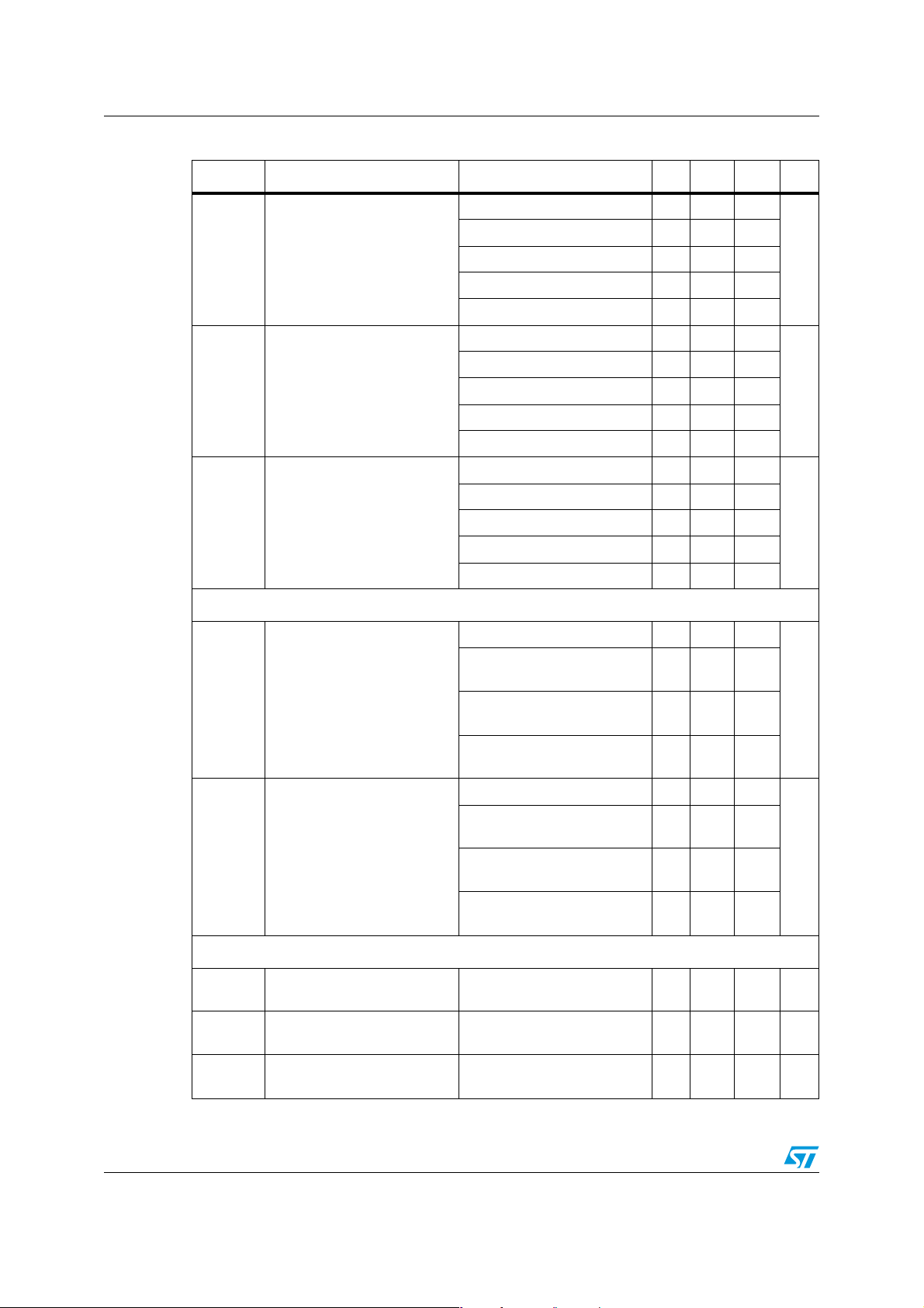
Electrical characteristics L6472
Table 5. Electrical characteristics (continued)
Symbol Parameter Test condition Min. Typ. Max. Unit
(3)
SR
SR
t
Fall time
f
Output rising slew rate
out_r
Output falling slew rate
out_f
Dead time and blanking
POW_SR = '00'; I
POW_SR = '00'; I
POW_SR = ‘11’, I
POW_SR = ‘10’, I
POW_SR = ‘01’, I
POW_SR = '00', I
POW_SR = '00', I
POW_SR = ‘11’, I
POW_SR = ‘10’, I
POW_SR = ‘01’, I
POW_SR = '00', I
POW_SR = '00', I
POW_SR = ‘11’, I
POW_SR = ‘10’, I
POW_SR = ‘01’, I
= +1A 90
out
= -1A 110
out
= ±1A 110
out
= ±1A 260
out
= ±1A 375
load
= +1A 285
out
= -1A 360
out
= ±1A 285
out
= ±1A 150
out
= ±1A 95
out
= +1A 320
out
= -1A 260
out
= ±1A 260
out
= ±1A 110
out
= ±1A 75
out
POW_SR = '00' 250
ns
V/µs
V/µs
t
t
blank Blanking time
DT
Dead time
Source-drain diodes
High-side diode forward ON
V
SD,HS
V
SD,LS
t
rrHS
voltage
Low-side diode forward ON
voltage
High-side diode reverse
recovery time
(1)
(1)
POW_SR = ‘11’,
= 16MHz
f
OSC
POW_SR = ‘10’,
f
= 16MHz
OSC
POW_SR = ‘01’,
= 16MHz
f
OSC
375
625
875
POW_SR = '00' 250
POW_SR = ‘11’,
= 16MHz
f
OSC
POW_SR = ‘10’,
= 16MHz
f
OSC
POW_SR = ‘01’,
f
= 16MHz
OSC
= 1A 1 1.1 V
I
out
I
= 1A 1 1.1 V
out
= 1A 30 ns
I
out
375
625
875
ns
ns
12/69 Doc ID 022729 Rev 1
Page 13
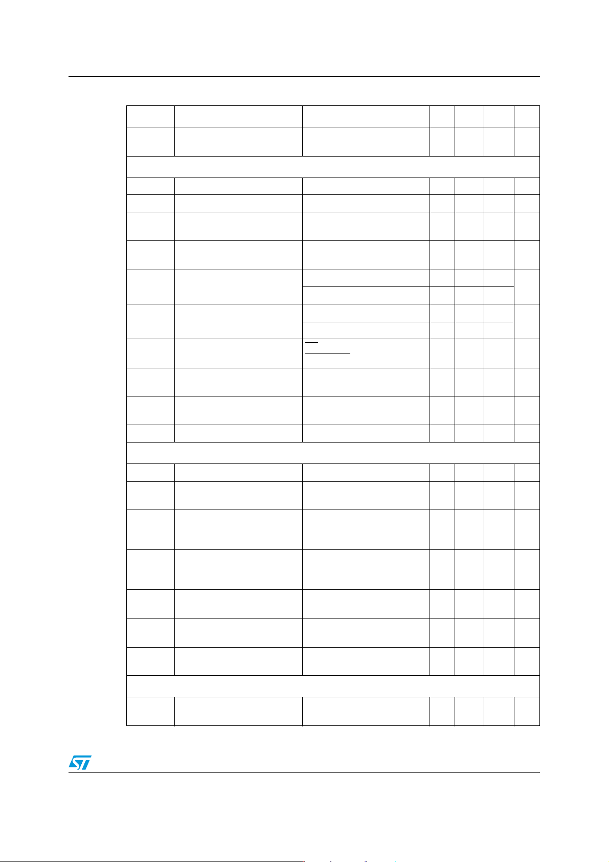
L6472 Electrical characteristics
Table 5. Electrical characteristics (continued)
Symbol Parameter Test condition Min. Typ. Max. Unit
t
rrLS
Low-side diode reverse
recovery time
= 1A 100 ns
I
out
Logic inputs and outputs
Low logic level input voltage 0.8 V
V
IL
V
High logic level input voltage 2 V
IH
I
IIL
VOL
VOH High logic level output voltage
High logic level input current
(4)
IH
Low logic level input current
(5)
Low logic level output voltage
(6)
VIN = 5V 1 µA
V
= 0V -1 µA
IN
VDD = 3.3V, IOL = 4mA 0.3
= 5V, IOL = 4mA 0.3
V
DD
V
= 3.3V, IOH = 4mA 2.4
DD
VDD = 5V, IOH = 4mA 4.7
R
R
I
logic
I
logic,STBY
CS pull-up and STBY pull-
PU
down resistors
PD
Internal logic supply current
Standby mode internal logic
supply current
CS
= GND;
STBY/RST
3.3V V
= 5V
externally
REG
supplied, internal oscillator
3.3V V
externally supplied 2 2.5 µA
REG
335 430 565 kΩ
3.7 4.3 mA
V
V
f
Step-clock input frequency 2 MHz
STCK
Internal oscillator and external oscillator driver
Internal oscillator frequency T
f
osc,i
f
osc,e
V
OSCOUT
V
OSCOUTL
t
rOSCOUT
t
fOSCOUT
t
extosc
t
intosc
Programmable external
oscillator frequency
OSCOUT clock source high
level voltage
H
OSCOUT clock source low
level voltage
OSCOUT clock source rise
and fall time
Internal to external oscillator
switching delay
External to internal oscillator
switching delay
= 25°C, V
j
Internal oscillator 3.3V V
externally supplied; I
= 4mA
Internal oscillator 3.3V V
externally supplied; I
= 4mA
Internal oscillator 20 ns
SPI
Maximum SPI clock
f
CK,MAX
frequency
(7)
= 3.3V -3% 16 +3% MHz
REG
8 32 MHz
REG
OSCOUT
REG
OSCOUT
2.4 V
0.3 V
3 ms
1.5 µs
5 MHz
Doc ID 022729 Rev 1 13/69
Page 14
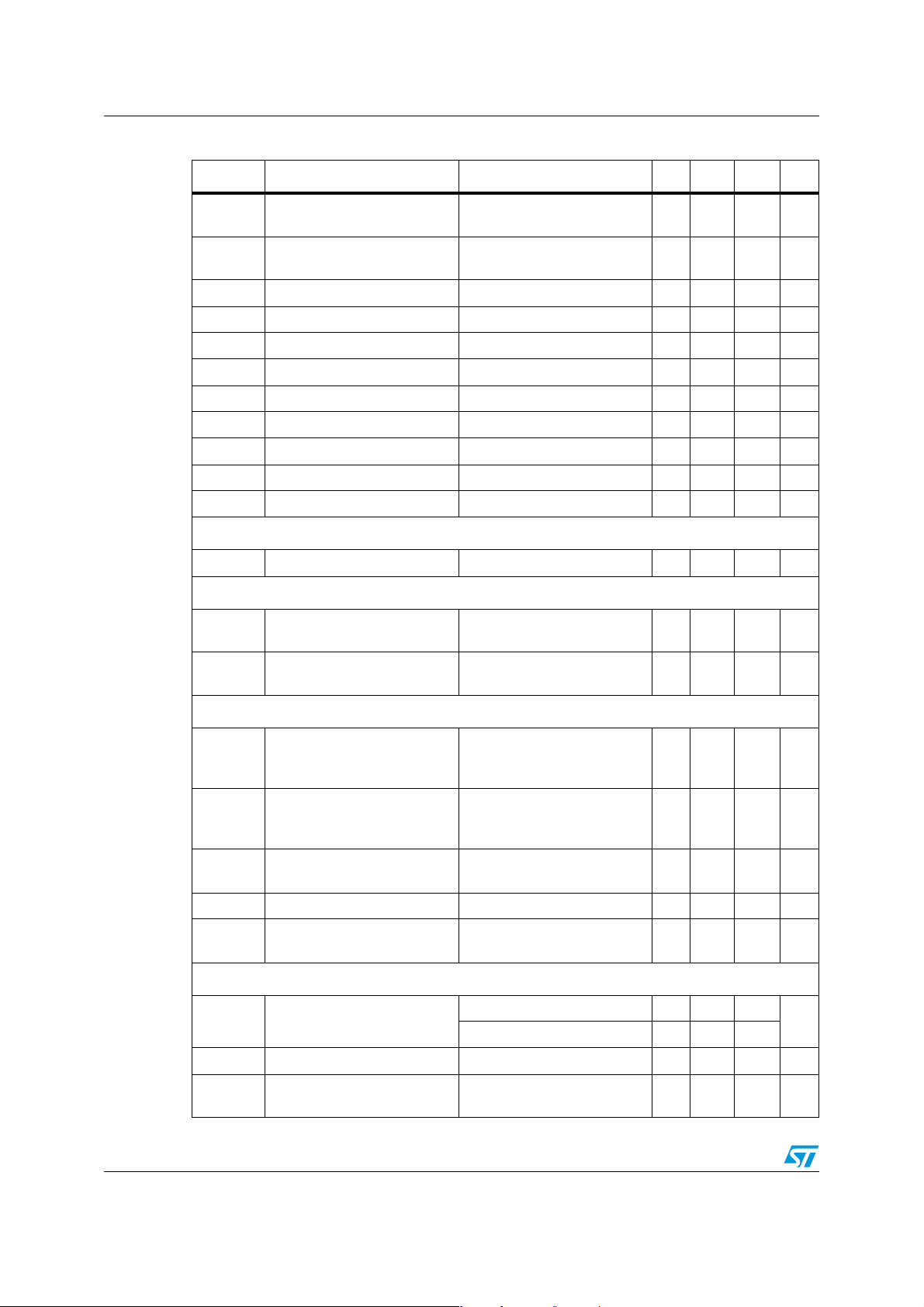
Electrical characteristics L6472
Table 5. Electrical characteristics (continued)
Symbol Parameter Test condition Min. Typ. Max. Unit
t
rCK
t
fCK
t
hCK
t
lCK
t
setCS
t
holCS
t
disCS
t
setSDI
t
holSDI
t
enSDO
t
disSDO
t
vSDO
t
holSDO
SPI clock rise and fall time
SPI clock high and low time
(7)
Chip select setup time
Chip select hold time
De-select time
Data input setup time
Data input hold time
Data output enable time
Data output disable time
Data output valid time
Data output hold time
Switch input (SW)
R
PUSW
SW input pull-up resistance SW = GND 60 85 110 kΩ
Current control
I
STEP,max
Max. programmable
reference current
(7)
(7)
CL = 30pF 25 ns
75 ns
(7)
(7)
350 ns
10 ns
800 ns
(7)
(7)
(7)
(7)
(7)
(7)
37 ns
25 ns
20 ns
38 ns
47 ns
57 ns
4 A
I
STEP,min
Min. programmable reference
current
Overcurrent protection
Maximum programmable
I
OCD,MAX
overcurrent detection
threshold
Minimum programmable
I
OCD,MIN
overcurrent detection
threshold
I
OCD,RES
t
OCD,Flag
t
OCD,SD
Programmable overcurrent
detection threshold resolution
OCD to flag signal delay time dI
OCD to shutdown delay time
Standby
Quiescent motor supply
I
qSTBY
t
STBY,min
t
logicwu
current in standby conditions
Minimum standby time 10 µs
Logic power-on and wake-up
time
31 mA
OCD_TH = ‘1111’ 6 A
OCD_TH = ‘0000’
= 350A/µs 650 1000 ns
out/dt
= 350A/µs POW_SR =
dI
out/dt
'10'
= 8V 26 34
V
S
S = 36V 30 36
V
0.37
5
0.37
5
A
A
600 µs
µA
38 45 µs
14/69 Doc ID 022729 Rev 1
Page 15
L6472 Electrical characteristics
Table 5. Electrical characteristics (continued)
Symbol Parameter Test condition Min. Typ. Max. Unit
t
cpwu
Charge pump power-on and
wake-up time
Power bridges disabled, Cp =
10nF, C
= 220nF
boot
Internal voltage regulator
REG
I
REG
V
REG, drop
I
REG,STBY
voltage
Voltage regulator output
current
Voltage regulator output
voltage drop
Voltage regulator standby
output current
= 40mA 50 mV
I
REG
Voltage regulator output
V
Integrated analog-to-digital converter
Analog-to-digital converter
N
ADC
V
ADC,ref
1. Accuracy depends on oscillator frequency accuracy.
2. Tested at 25 °C in a restricted range and guaranteed by characterization.
3. Rise and fall time depends on motor supply voltage value. Refer to SR
actual rise and fall time.
4. Not valid for the STBY/RST
5. Not valid for the SW and CS pins which have an internal pull-up resistor.
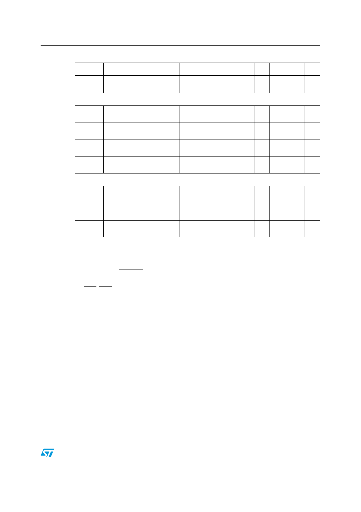
6. FLAG
7. See Figure 20 – SPI timings diagram for details.
resolution
Analog-to-digital converter
reference voltage
Analog-to-digital converter
f
S
sampling frequency
pin which has an internal pull-down resistor.
, BUSY and SYNC open drain outputs included.
out
650 µs
2.9 3 3.2 V
40 mA
10 mA
5 bit
V
V
REG
f
/
OSC
512
values in order to evaluate the
kHz
Doc ID 022729 Rev 1 15/69
Page 16

Pin connection L6472
4 Pin connection
Figure 2. HTSSOP28 pin connection (top view)
345
Figure 3. POWERSO36 pin connection (top view)
74"
74"
48
&1"%
1(/%
065"
065"
45#:345
"%$*/
73&(
04$*/
04$065
"(/%
$1
7#005
065#
065#
74#
74#
065"
065"
74"
74"
45$,
'-"(
$4
#64:=4:/$
%(/%
4%*
$,
4%0
7%%
74#
74#
065#
065#
1(/%
16/69 Doc ID 022729 Rev 1
Page 17
L6472 Pin connection
4.1 Pin list
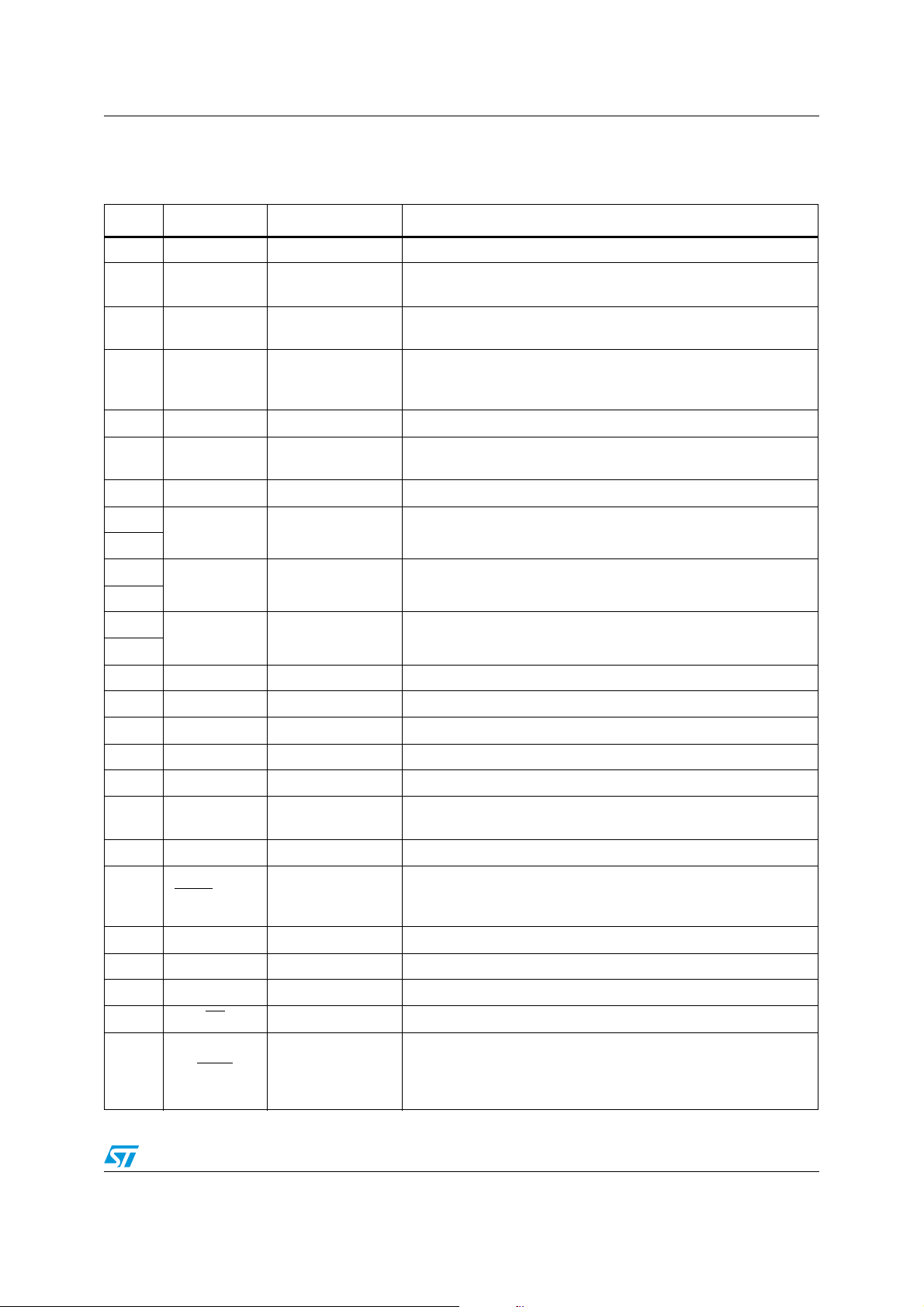
Table 6. Pin description
No. Name Type Function
17 VDD Power Logic output supply voltage (pull-up reference)
6 VREG Power
7 OSCIN Analog input
Internal 3 V voltage regulator output and 3.3 V external logic
supply
Oscillator pin 1. To connect an external oscillator or clock source.
If this pin is unused, it should be left floating.
Oscillator pin 2. To connect an external oscillator. When the
8 OSCOUT Analog output
internal oscillator is used this pin can supply 2/4/8/16 MHz. If this
pin is unused, it should be left floating.
10 CP Output Charge pump oscillator output
11 Vboot Supply voltage
Bootstrap voltage needed for driving the high-side power DMOS of
both bridges (A and B)
5 ADCIN Analog input Internal analog-to-digital converter input
2
VSA Power supply Full bridge A power supply pin. It must be connected to VSB
26
12
VSB Power supply Full bridge B power supply pin. It must be connected to VSA
16
27
PGND Ground Power ground pin
13
1 OUT1A Power output Full bridge A output 1
28 OUT2A Power output Full bridge A output 2
14 OUT1B Power output Full bridge B output 1
15 OUT2B Power output Full bridge B output 2
9 AGND Ground Analog ground.
4 SW Logical input
External switch input pin. If not used the pin should be connected
to VDD.
21 DGND Ground Digital ground
By default, this BUSY pin is forced low when the device is
22 BUSY
\SYNC Open drain output
performing a command. Otherwise the pin can be configured to
generate a synchronization signal.
18 SDO Logic output Data output pin for serial interface
20 SDI Logic input Data input pin for serial interface
19 CK Logic input Serial interface clock
23 CS
Logic input Chip select input pin for serial interface
Status flag pin. An internal open drain transistor can pull the pin to
24 FLAG Open drain output
GND when a programmed alarm condition occurs (step loss,
OCD, thermal pre-warning or shutdown, UVLO, wrong command,
non-performable command)
Doc ID 022729 Rev 1 17/69
Page 18

Pin connection L6472
Table 6. Pin description (continued)
No. Name Type Function
Standby and reset pin. LOW logic level resets the logic and puts
3 STBY\RST Logic input
25 STCK Logic input Step-clock input
EPAD Exposed pad Ground Internally connected to PGND, AGND and DGND pins
the device into standby mode. If not used, it should be connected
to VDD
18/69 Doc ID 022729 Rev 1
Page 19
L6472 Typical applications
5 Typical applications
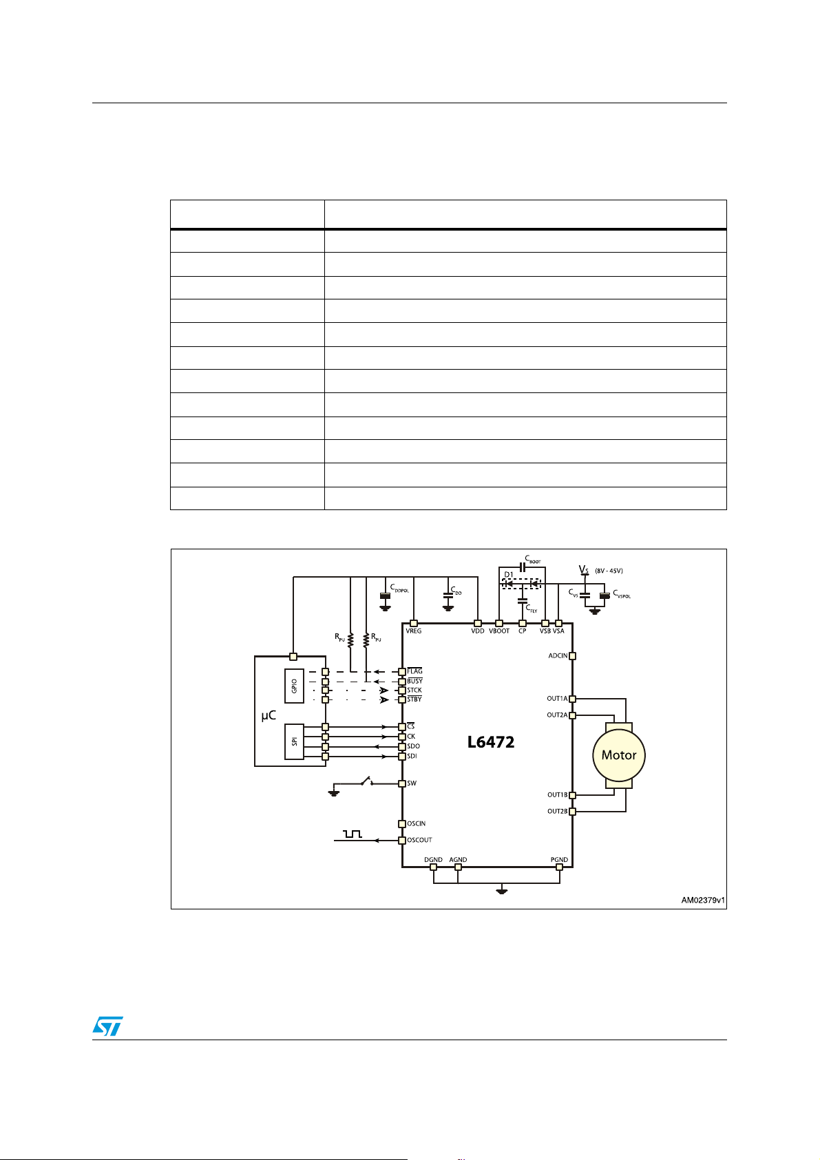
Table 7. Typical application values
Name Value
220 nF
C
VS
C
C
C
100 µF
VSPOL
C
100 nF
REG
REGPOL
47 µF
C
100 nF
DD
10 µF
DDPOL
D1 Charge pump diodes
C
220 nF
BOOT
C
10 nF
FLY
R
39 kΩ
PU
R
100 Ω
SW
CSW 10 nF
Figure 4. Bipolar stepper motor control application using the L6472
Doc ID 022729 Rev 1 19/69
Page 20

Functional description L6472
6 Functional description
6.1 Device power-up
At the end of power-up, the device state is the following:
● Registers are set to default,
● Internal logic is driven by the internal oscillator and a 2 MHz clock is provided by the
OSCOUT pin,
● Bridges are disabled (High Z),
● UVLO bit in the STATUS register is forced low (fail condition),
● FLAG output is forced low.
During power-up the device is under reset (all logic IO disabled and power bridges in highimpedance state) until the following conditions are satisfied:
● V
●
● Internal oscillator is operative.
Any motion command causes the device to exit from High Z state (HardStop and SoftStop
included).
is greater than V
S
V
is greater than V
REG
SthOn
REGth
= 2.8 V (typ.)
6.2 Logic I/O
Pins CS, CK, SDI, STCK, SW and STBY\RST are TTL/CMOS 3.3 V-5 V compatible logic
inputs.
Pin SDO is a TTL/CMOS compatible logic output. The VDD pin voltage sets the logic output
pin voltage range; when it is connected to VREG or a 3.3 V external supply voltage, the
output is 3.3 V compatible. When VDD is connected to a 5 V supply voltage, SDO is 5 V
compatible.
VDD is not internally connected to V
A 10 µF capacitor should be connected to the VDD pin in order to obtain a proper operation.
Pins FLAG
and BUSY\SYNC are open drain outputs.
6.3 Charge pump
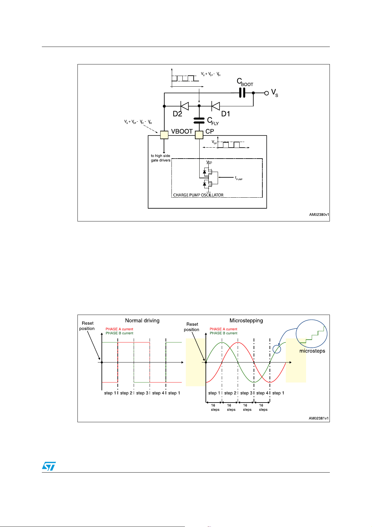
To ensure the correct driving of the high-side integrated MOSFETs, a voltage higher than
the motor power supply voltage needs to be applied to the Vboot pin. The high-side gate
driver supply voltage Vboot is obtained through an oscillator and a few external components
realizing a charge pump (see Figure 5).
, an external connection is always needed.
REG
20/69 Doc ID 022729 Rev 1
Page 21
L6472 Functional description
Figure 5. Charge pump circuitry
6.4 Microstepping
The driver is able to divide the single step into up to 16 microsteps. Step mode can be
programmed by the STEP_SEL parameter in the STEP_MODE register (see Ta b le 1 9 ).
Step mode can only be changed when bridges are disabled. Every time step mode is
changed, the electrical position (i.e. the point of microstepping sinewave that is generated)
is reset to the first microstep, and the absolute position counter value (see Section 6.5)
becomes meaningless.
Figure 6. Normal mode and microstepping (16 microsteps)
Doc ID 022729 Rev 1 21/69
Page 22
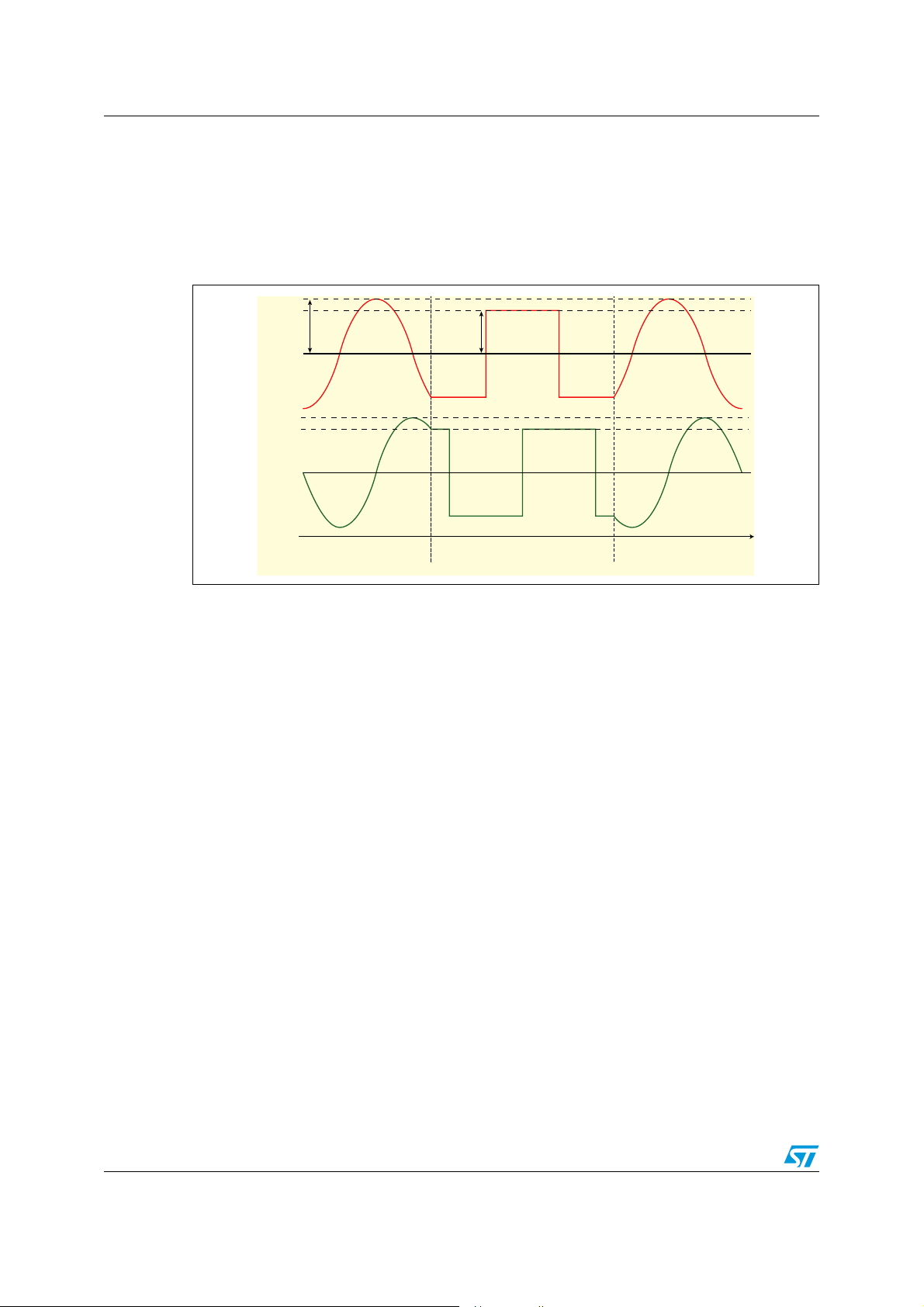
Functional description L6472
6.4.1 Automatic full-step mode
When motor speed is greater than a programmable full-step speed threshold, the L6472
switches automatically to full-step mode (see Figure 7); the driving mode returns to
microstepping when motor speed decreases below the full-step speed threshold. The fullstep speed threshold is set through the FS_SPD register (see Section 9.1.9).
Figure 7. Automatic full-step switching
)
PEAK
0HASE!
0HASE"
SINPX)
PEAK
M3TEPPING
.XP .XP
6.5 Absolute position counter
An internal 22-bit register (ABS_POS) keeps track of the motor motion according to the
selected step mode; the stored value unit is equal to the selected step mode (full, half,
quarter, etc.). The position range is from -2
6.6 Programmable speed profiles
The user can easily program a customized speed profile, independently defining
acceleration, deceleration, maximum and minimum speed values through the ACC, DEC,
MAX_SPEED and MIN_SPEED registers respectively (see Section 9.1.5, 9.1.6, 9.1.7 and
9.1.8).
When a command is sent to the device, the integrated logic generates the microstep
frequency profile that performs a motor motion compliant to speed profile boundaries.
All acceleration parameters are expressed in step/tick
expressed in step/tick; the unit of measurement does not depend on selected step mode.
Acceleration and deceleration parameters range from 2
(equivalent to 14.55 to 59590 step/s2).
Minimum speed parameter ranges from 0 to (2
step/s).
Maximum speed parameter ranges from 2
15610 step/s).
-18
&ULL3TEP
21
to +221-1 (µ) steps (see Section 9.1.1).
2
and all speed parameters are
-40
to (212-2)•2
12
-24
-1)•2
step/tick (equivalent to 0 to 976.3
to (2
10
-1)• 2
-18
step/tick (equivalent to 15.25 to
M3TEPPING
-40
step/tick2
22/69 Doc ID 022729 Rev 1
Page 23
L6472 Functional description
6.6.1 Infinite acceleration/deceleration mode
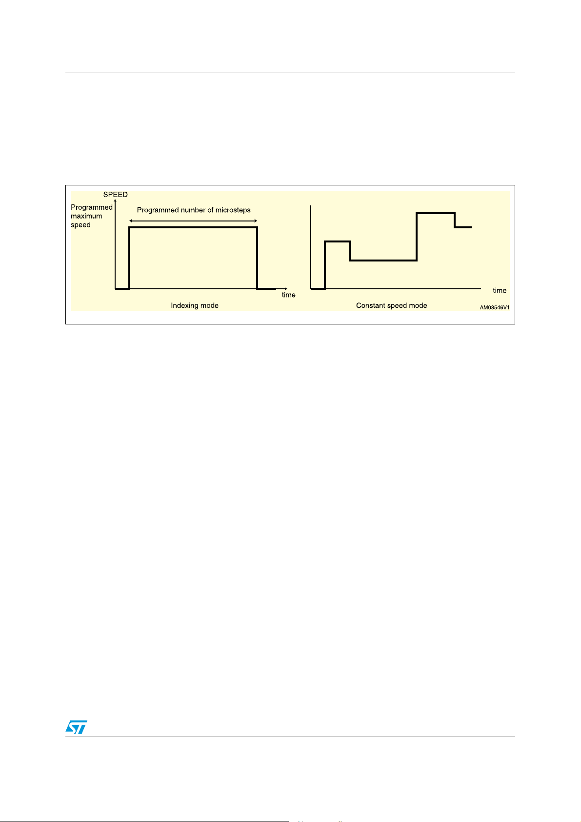
When the ACC register value is set to max. (0xFFF), the system works in “infinite
acceleration mode”: acceleration and deceleration phases are totally skipped, as shown in
Figure 8.
It is not possible to skip the acceleration or deceleration phase independently.
Figure 8. Speed profile in infinite acceleration/deceleration mode
6.7 Motor control commands
The L6472 can accept different types of commands:
● constant speed commands (Run, GoUntil, ReleaseSW)
● absolute positioning commands (GoTo, GoTo_DIR, GoHome, GoMark)
● motion commands (Move)
● stop commands (SoftStop, HardStop, SoftHiz, HardHiz).
For detailed command descriptions refer to Section 9.2.
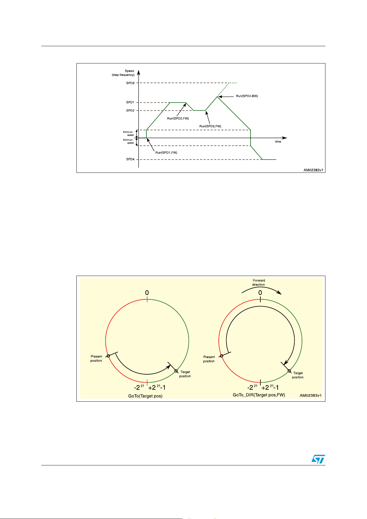
6.7.1 Constant speed commands
A constant speed command produces a motion in order to reach and maintain a user
defined target speed starting from the programmed minimum speed (set in the MIN_SPEED
register) and with the programmed acceleration/deceleration value (set in the ACC and DEC
registers). A new constant speed command can be requested anytime.
Doc ID 022729 Rev 1 23/69
Page 24
Functional description L6472
Figure 9. Constant speed commands examples
6.7.2 Positioning commands
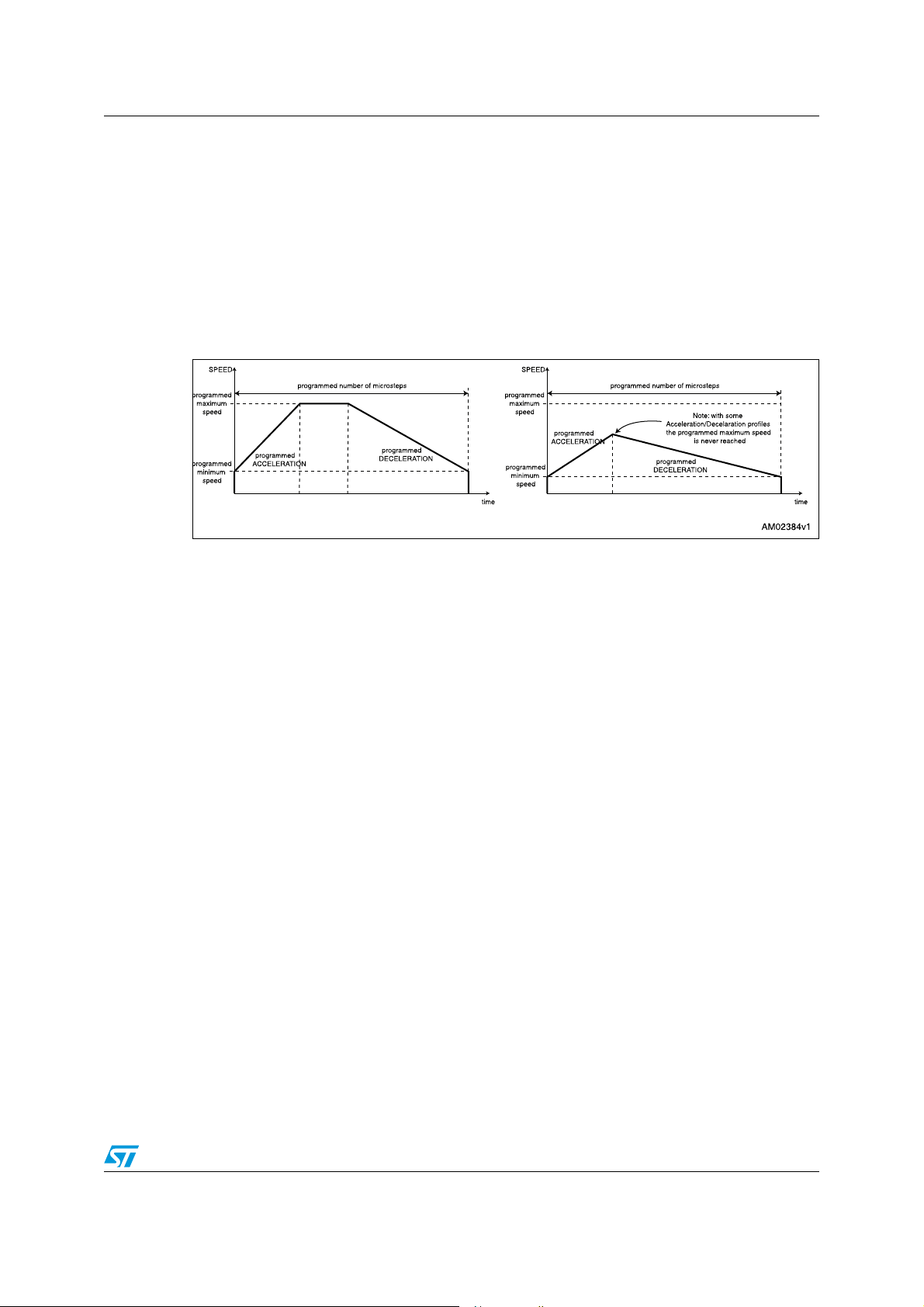
An absolute positioning command produces a motion in order to reach a user-defined
position that is sent to the device together with the command. The position can be reached
by performing the minimum path (minimum physical distance) or forcing a direction (see
Figure 10).
The performed motor motion is compliant to programmed speed profile boundaries
(acceleration, deceleration, minimum and maximum speed).
Note that with some speed profiles or positioning commands, the deceleration phase can
start before the maximum speed is reached.
Figure 10. Positioning command examples
24/69 Doc ID 022729 Rev 1
Page 25
L6472 Functional description
6.7.3 Motion commands
Motion commands produce a motion in order to perform a user-defined number of
microsteps in a user-defined direction that are sent to the device together with the command
(see Figure 11).
The performed motor motion is compliant to programmed speed profile boundaries
(acceleration, deceleration, minimum and maximum speed).
Note that with some speed profiles or motion commands, the deceleration phase can start
before the maximum speed is reached.
Figure 11. Motion command examples
6.7.4 Stop commands
A stop command forces the motor to stop. Stop commands can be sent anytime.
The SoftStop command causes the motor to decelerate with a programmed deceleration
value until the MIN_SPEED value is reached and then stops the motor maintaining the rotor
position (a holding torque is applied).
The HardStop command stops the motor instantly, ignoring deceleration constraints and
maintaining the rotor position (a holding torque is applied).
The SoftHiZ command causes the motor to decelerate with a programmed deceleration
value until the MIN_SPEED value is reached and then forces the bridges into highimpedance state (no holding torque is present).
The HardHiZ command instantly forces the bridges into high-impedance state (no holding
torque is present).
6.7.5 Step-clock mode
In step-clock mode the motor motion is defined by the step-clock signal applied to the STCK
pin.
At each step-clock rising edge, the motor is moved by one microstep in the programmed
direction and the absolute position is consequently updated.
When the system is in step-clock mode the SCK_MOD flag in the STATUS register is raised,
the SPEED register is set to zero and the motor status is considered stopped whatever the
STCK signal frequency (the MOT_STATUS parameter in the STATUS register equal to
g00h).
Doc ID 022729 Rev 1 25/69
Page 26

Functional description L6472
6.7.6 GoUntil and ReleaseSW commands
In most applications the power-up position of the stepper motor is undefined, so an
initialization algorithm driving the motor to a known position is necessary.
The GoUntil and ReleaseSW commands can be used in combination with external switch
input (see Section 6.13) to easily initialize the motor position.
The GoUntil command makes the motor run at the target constant speed until the SW input
is forced low (falling edge). When this event occurs, one of the following actions can be
performed:
● ABS_POS register is set to zero (home position) and the motor decelerates to zero
speed (as a SoftStop command)
● ABS_POS register value is stored in the MARK register and the motor decelerates to
zero speed (as a SoftStop command).
If the SW_MODE bit of the CONFIG register is set to e0f, the motor does not decelerate but
it immediately stops (as a HardStop command).
The ReleaseSW command makes the motor run at the programmed minimum speed until
the SW input is forced high (rising edge). When this event occurs, one of the following
actions can be performed:
● ABS_POS register is set to zero (home position) and the motor immediately stops (as a
HardStop command)
● ABS_POS register value is stored in the MARK register and the motor immediately
stops (as a HardStop command).
If the programmed minimum speed is less than 5 step/s, the motor is driven at 5 step/s.
26/69 Doc ID 022729 Rev 1
Page 27
L6472 Functional description
6.8 Internal oscillator and oscillator driver
The control logic clock can be supplied by the internal 16-MHz oscillator, an external
oscillator (crystal or ceramic resonator) or a direct clock signal.
These working modes can be selected by the EXT_CLK and OSC_SEL parameters in the
CONFIG register (see Ta b le 2 4 ).
At power-up the device starts using the internal oscillator and provides a 2-MHz clock signal
on the OSCOUT pin.
Attention: In any case, before changing clock source configuration, a
hardware reset is mandatory. Switching to different clock
configurations during operation could cause unexpected
behavior.
6.8.1 Internal oscillator
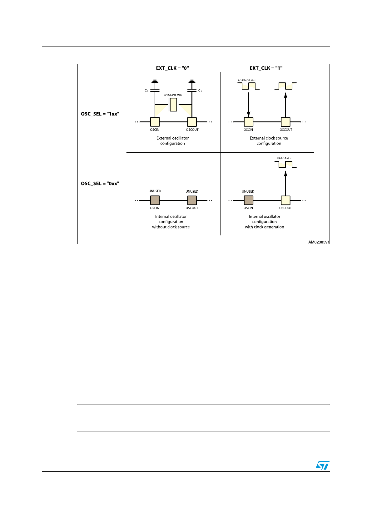
In this mode the internal oscillator is activated and OSCIN is unused. If the OSCOUT clock
source is enabled, the OSCOUT pin provides a 2, 4, 8 or 16-MHz clock signal (according to
the OSC_SEL value); otherwise it is unused (see Figure 12).
6.8.2 External clock source
Two types of external clock source can be selected: crystal/ceramic resonator or direct clock
source. Four programmable clock frequencies are available for each external clock source:
8, 16, 24 and 32 MHz.
When an external crystal/resonator is selected, the OSCIN and OSCOUT pins are used to
drive the crystal/resonator (see Figure 12). The crystal/resonator and load capacitors (CL)
must be placed as close as possible to the pins. Refer to Ta bl e 8 for the choice of the load
capacitor value according to the external oscillator frequency.
Table 8. CL values according to external oscillator frequency
Crystal/resonator freq.
8 MHz 25 pF (ESR
16 MHz 18 pF (ESR
24 MHz 15 pF (ESR
32 MHz 10 pF (ESR
1. First harmonic resonance frequency.
2. Lower ESR value allows the driving of greater load capacitors.
If a direct clock source is used, it must be connected to the OSCIN pin, and the OSCOUT
pin supplies the inverted OSCIN signal (see Figure 12).
(1)
CL
(2)
max
max
max
max
= 80 Ω)
= 50 Ω)
= 40 Ω)
= 40 Ω)
Doc ID 022729 Rev 1 27/69
Page 28
Functional description L6472
Figure 12. OSCIN and OSCOUT pin configurations
Note: When OSCIN is UNUSED, it should be left floating.
When OSCOUT is UNUSED it should be left floating.
6.9 Overcurrent detection
When the current in any of the Power MOSFETs exceeds a programmed overcurrent
threshold, the STATUS register OCD flag is forced low until the overcurrent event expires
and a GetStatus command is sent to the IC (see Section 9.1.19 and 9.2.20). The
overcurrent event expires when all the Power MOSFET currents fall below the programmed
overcurrent threshold.
The overcurrent threshold can be programmed through the OCD_TH register in one of 16
available values ranging from 375 mA to 6 A with steps of 375 mA (see Ta bl e 1 7 ).
It is possible to set if an overcurrent event causes or not the MOSFET turn-off (bridges in
high-impedance status) acting on the OC_SD bit in the CONFIG register (see
Section 9.1.18). The OCD flag in the STATUS register is raised anyway (see Ta bl e 2 5 ).
When the IC outputs are turned-off by an OCD event, they cannot be turned on until the
OCD flag is released by a GetStatus command.
Attention: The overcurrent shutdown is a critical protection feature. It is
not recommended to disable it.
28/69 Doc ID 022729 Rev 1
Page 29

L6472 Functional description
6.10 Undervoltage lockout (UVLO)
The L6472 provides motor supply UVLO protection. When the motor supply voltage falls
below the VSthOff threshold voltage, the STATUS register UVLO flag is forced low. When a
GetStatus command is sent to the IC, and the undervoltage condition expires, the UVLO
flag is released (see Section 9.1.19 and 9.2.20). The undervoltage condition expires when
the motor supply voltage goes over the VSthOn threshold voltage. When the device is in the
undervoltage condition, no motion command can be performed. The UVLO flag is forced low
by logic reset (power-up included) even if no UVLO condition is present.
6.11 Thermal warning and thermal shutdown
An internal sensor allows the L6472 to detect when the device internal temperature exceeds
a thermal warning or an overtemperature threshold.
When the thermal warning threshold (T
register is forced low (see Section 9.1.19) until the temperature decreases below T
and a GetStatus command is sent to the IC (see Section 9.1.19 and 9.2.20).
When the thermal shutdown threshold (T
shutdown condition: the TH_SD bit in the STATUS register is forced low, the power bridges
are disabled bridges in high-impedance state and the HiZ bit in the STATUS register is
raised (see Section 9.1.19).
The thermal shutdown condition only expires when the temperature goes below the thermal
warning threshold (T
On exiting the thermal shutdown condition, the bridges are still disabled (HiZ flag high);
whichever motion command makes the device exit from High Z state (HardStop and
SoftStop included).
j(WRN)
6.12 Reset and standby
The device can be reset and put into standby mode through a dedicated pin. When the
STBY
\RST pin is driven low, the bridges are left open (High Z state), the internal charge
pump is stopped, the SPI interface and control logic are disabled, and the internal 3 V
voltage regulator maximum output current is reduced to IREG,STBY; as a result, the L6472
heavily reduces the power consumption. At the same time the register values are reset to
default and all protection functions are disabled. STBY\RST
least for tSTBY,min, in order to ensure the complete switch to standby mode.
) is reached, the TH_WRN bit in the STATUS
j(WRN)
) is reached, the device goes into the thermal
j(OFF)
).
input must be forced low at
j(WRN)
On exiting standby mode, as well as for IC power-up, a delay of up to tlogicwu must be given
before applying a new command to allow proper oscillator and logic startup and a delay of
up to tcpwu must be given to allow the charge pump startup.
On exiting standby mode the bridges are disabled (HiZ flag high) and whichever motion
command causes the device to exit High Z state (HardStop and SoftStop included).
Attention: It is not recommended to reset the device when outputs are
active. The device should be switched to high-impedance
state before being reset.
Doc ID 022729 Rev 1 29/69
Page 30
Functional description L6472
6.13 External switch (SW pin)
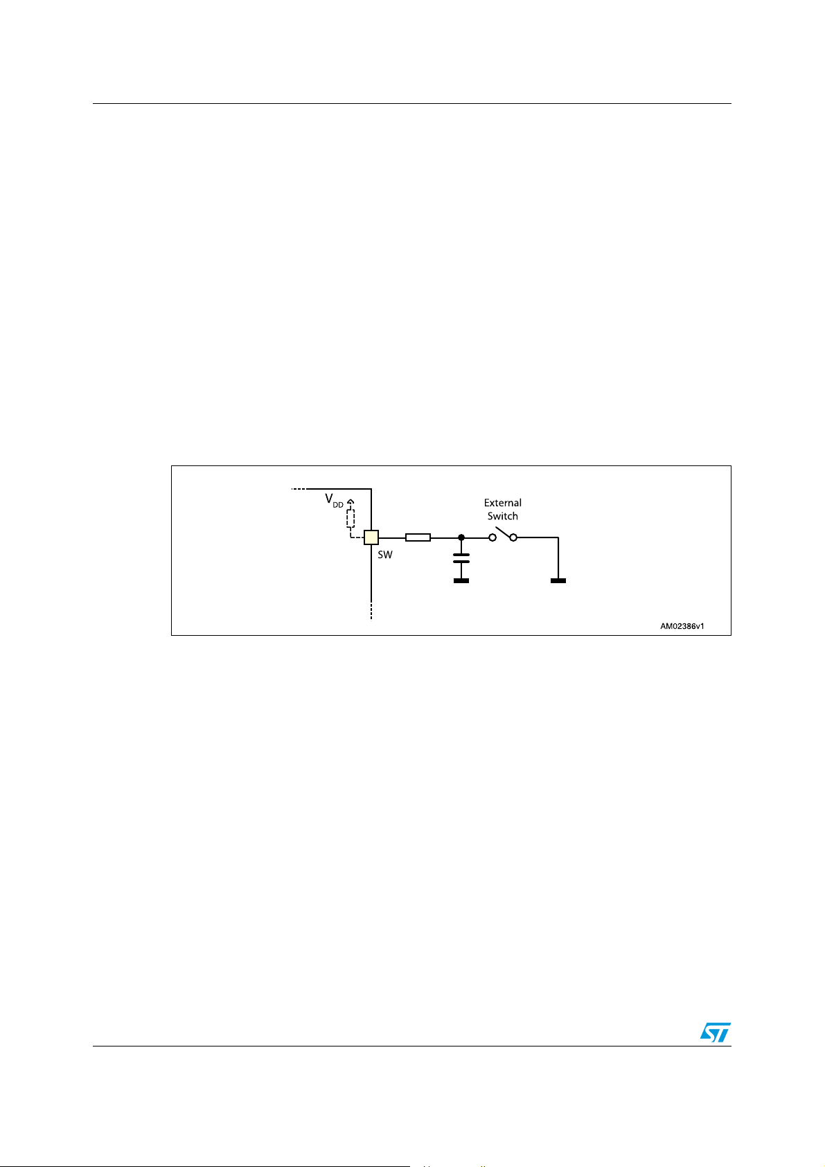
The SW input is internally pulled-up to VDD and detects if the pin is open or connected to
ground (see Figure ).
The SW_F bit of the STATUS register indicates if the switch is open (‘0’) or closed (‘1’) (see
Section 9.1.19); the bit value is refreshed at every system clock cycle (125 ns). The
SW_EVN flag of the STATUS register is raised when a switch turn-on event (SW input falling
edge) is detected (see Section 9.1.19). A GetStatus command releases the SW_EVN flag
(see Section 9.2.20).
By default a switch turn-on event causes a HardStop interrupt (SW_MODE bit of the
CONFIG register set to ‘0’). Otherwise (SW_MODE bit of the CONFIG register set to ‘1’),
switch input events do not cause interrupts and the switch status information is at the user’s
disposal (see Ta b le 2 5 ).
The switch input can be used by the GoUntil and ReleaseSW commands as described in
Section 9.2.10 and 9.2.11.
If the SW input is not used, it should be connected to VDD.
Figure 13. External switch connection
6.14 Programmable DMOS slew rate, dead time and blanking time
Using the POW_SR parameter in the CONFIG register, it is possible to set the commutation
speed of the power bridge output (see Ta bl e 2 7).
6.15 Integrated analog-to-digital converter
The L6472 integrates an NADC bit ramp-compare analog-to-digital converter with a
reference voltage equal to VREG. The analog-to-digital converter input is available through
the ADCIN pin and the conversion result is available in the ADC_OUT register (see
Section 9.1.13). The sampling frequency is equal to the clock frequency divided by 512.
The ADC_OUT value can be used for the torque regulation or can remain at the user’s
disposal.
30/69 Doc ID 022729 Rev 1
Page 31
L6472 Functional description
6.16 Internal voltage regulator
The L6472 integrates a voltage regulator which generates a 3 V voltage starting from motor
power supply (VSA and VSB). In order to make the voltage regulator stable, at least 22 µF
should be connected between the VREG pin and ground (the suggested value is 47 µF).
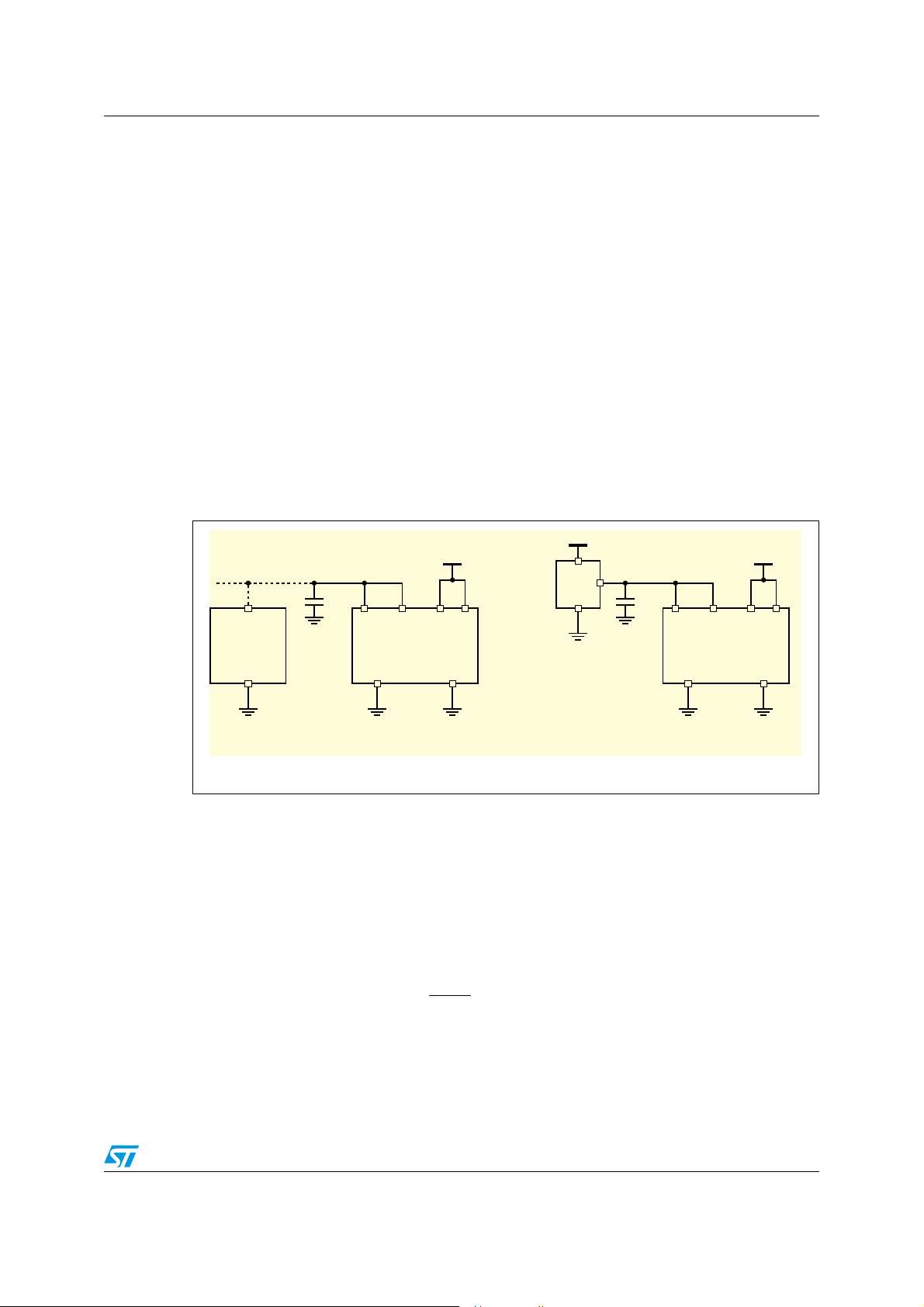
The internal voltage regulator can be used to supply the VDD pin in order to make the
device digital output range 3.3 V compatible (Figure 14). A digital output range 5 V
compatible can be obtained connecting the VDD pin to an external 5 V voltage source. In
both cases, a 10 µF capacitance should be connected to the VDD pin in order to obtain a
correct operation.
The internal voltage regulator is able to supply a current up to I
consumption included (I
can be supplied is I
REG, STBY
). When the device is in standby mode the maximum current that
logic
, internal consumption included (I
REG,MAX, internal logic
logic, STBY
).
If an external 3.3 V regulated voltage is available, it can be applied to the VREG pin in order
to supply all the internal logic and avoid power dissipation of the internal 3 V voltage
regulator (Figure 14). The external voltage regulator should never sink current from the
VREG pin.
Figure 14. Internal 3 V linear regulator
6"!4
)#
6
S
!'.$$'.$
6S
6
$$
6
M#
).4%2.!,VOLTAGEREGULATOR
62%' 6$$ 63! 63"
)#
!'.$$'.$
,OGIGSUPPLIEDBY
6
2%'
62%' 6$$ 63! 63"
,OGIGSUPPLIEDBY
%84%2.!,VOLTAGEREGULATOR
6.17 BUSY\SYNC pin
This pin is an open drain output which can be used as the busy flag or synchronization
signal according to the SYNC_EN bit value (STEP_MODE register).
6.17.1 BUSY operation mode
The pin works as busy signal when the SYNC_EN bit is set low (default condition). In this
mode the output is forced low while a constant speed, absolute positioning or motion
command is under execution. The BUSY
executed (target speed or target position reached). The STATUS register includes a BUSY
flag that is the BUSY pin mirror (see Section 9.1.19).
In the case of daisy chain configuration, BUSY pins of different ICs can be hard-wired to
save host controller GPIOs.
pin is released when the command has been
Doc ID 022729 Rev 1 31/69
Page 32

Functional description L6472
6.17.2 SYNC operation mode
The pin works as a synchronization signal when the SYNC_EN bit is set high. In this mode a
step-clock signal is provided on the output according to a SYNC_SEL and STEP_SEL
parameter combination (see Section 9.1.16).
6.18 FLAG pin
By default an internal open drain transistor pulls the FLAG pin to ground when at least one
of the following conditions occur:
● Power-up or standby/reset exit
● Overcurrent detection
● Thermal warning
● Thermal shutdown
● UVLO
● Switch turn-on event
● Wrong command
● Non-performable command.
It is possible to mask one or more alarm conditions by programming the ALARM_EN
register (see Ta bl e 2 2). If the corresponding bit of the ALARM_EN register is low, the alarm
condition is masked and it does not cause a FLAG pin transition; all other actions imposed
by alarm conditions are performed anyway. In the case of daisy chain configuration, the
FLAG pins of different ICs can be OR-wired to save host controller GPIOs.
32/69 Doc ID 022729 Rev 1
Page 33
L6472 Phase current control
7 Phase current control
The L6472 performs a new current control technique, named predictive current control,
allowing the device to obtain the target average phase current. This method is described in
detail in Section 7.1. Furthermore, the L6472 automatically selects the better decay mode in
order to follow the current profile.
Current control algorithm parameters can be programmed by the T_FAST, TON_MIN,
TOFF_MIN and CONFIG registers (see Section 9.1.11, 9.1.12, 9.1.13 and 9.1.18 for
details).
Different current amplitude can be set for acceleration, deceleration and constant speed
phases and when the motor is stopped through the TVAL_ACC, TVAL_DEC, TVAL_RUN
and TVAL_HOLD registers (see Section 7.4). The output current amplitude can also be
regulated by the ADCIN voltage value (see Section 6.15).
Each bridge is driven by an independent control system that shares the control parameters
only with other bridges.
7.1 Predictive current control
Unlike a classical peak current control system, that causes the phase current decay when
the target value is reached, this new method keeps the power bridge on for an extra time
after reaching the current threshold.
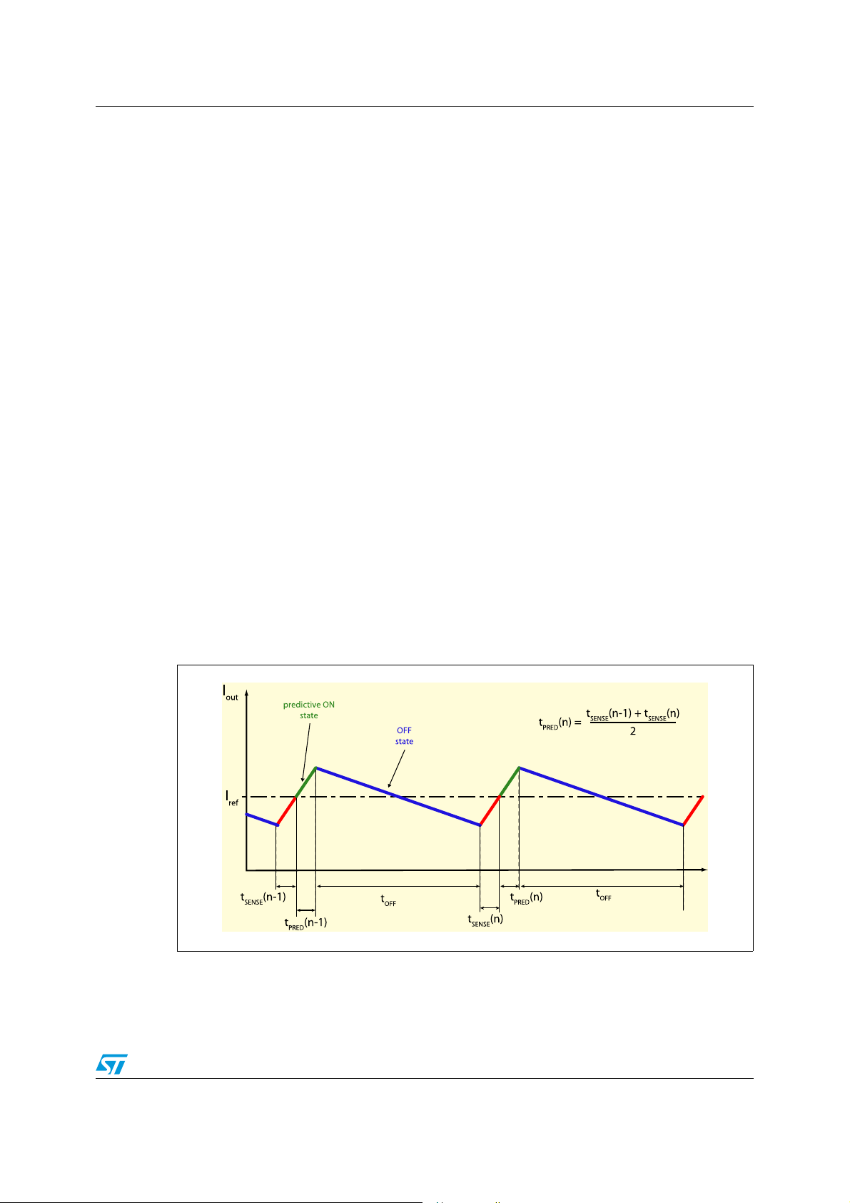
At each cycle the system measures the time required to reach the target current (t
After that the power stage is kept in a “predictive” ON state (t
mean value of t
in Figure 15.
Figure 15. Predictive current control
in the last two control cycles (actual one and previous one), as shown
SENSE
) for a time equal to the
PRED
SENSE
).
At the end of the predictive ON state the power stage is set in the OFF state for a fixed time,
as in a constant t
performed; the better decay combination is automatically selected by the L6472, as
described in Section 7.2.
current control. During the OFF state both slow and fast decay can be
OFF
Doc ID 022729 Rev 1 33/69
Page 34

Phase current control L6472
As shown in Figure 15, the system is able to center the triangular wave on the desired
reference value improving dramatically the accuracy of the current control system: in fact the
average value of a triangular wave is exactly equal to the middle point of each of its
segments and at steady-state the predictive current control tends to equalize the duration of
the t
SENSE
and the t
Furthermore, the t
time.
PRED
value is recalculated each time a new current value is requested
OFF
(microstep change) in order to keep the PWM frequency as near as possible to the
programmed one (TSW parameter in the CONFIG register).
The device can be forced to work using a classic peak current control setting the PRED_EN
bit in the CONFIG register low (default condition). In this case, after the sense phase
(t
) the power stage is set in the OFF state, as shown in Figure 16.
SENSE
Figure 16. Non-predictive current control
34/69 Doc ID 022729 Rev 1
Page 35
L6472 Phase current control
7.2 Auto-adjusted decay mode
During the current control, the device automatically selects the better decay mode in order
to follow the current profile reducing the current ripple.
At reset, the OFF time is performed by turning on both the low-side MOSFETs of the power
stage and the current recirculates in the lower half of the bridge (slow decay).
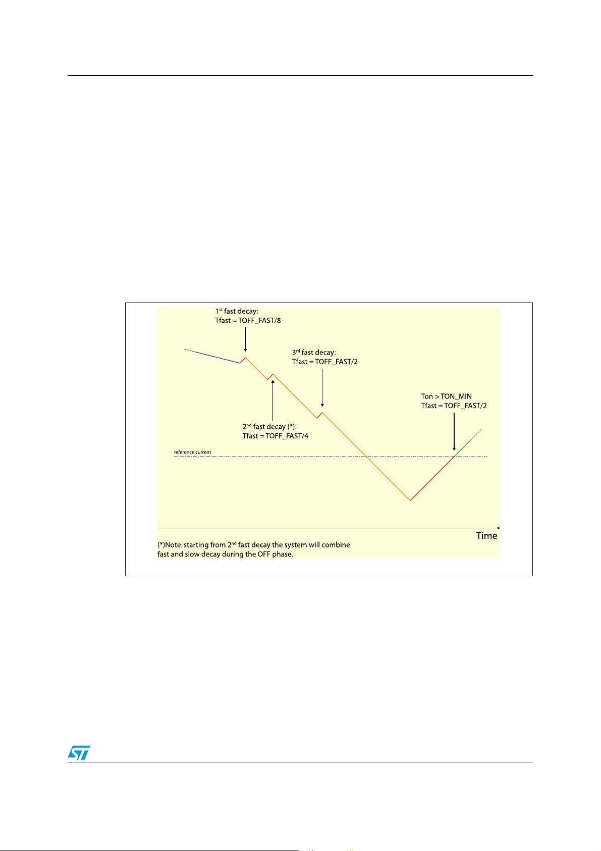
If, during a PWM cycle, the target current threshold is reached in a time shorter than the
TON_MIN value, a fast decay of TOFF_FAST/8 (T_FAST register) is immediately performed
turning on the opposite MOS of both half bridges and the current recirculates back to the
supply bus.
After this time, the bridge returns to the ON state: if the time needed to reach the target
current value is still less than TON_MIN, a new fast decay is performed with a period twice
the previous one. Otherwise, the normal control sequence is followed as described in
Section 7.1. The maximum fast decay duration is set by the TOFF_FAST value.
Figure 17. Adaptive decay - fast decay tuning
When two or more fast decays are performed with the present target current, the control
system adds a fast decay at the end of every OFF time, keeping the OFF state duration
constant (t
is split into t
OFF
OFF,SLOW
and t
OFF,FAST
). When the current threshold is increased
by a microstep change (rising step), the system returns to normal decay mode (slow decay
only) and the t
value is halved.
FAST
Stopping the motor or reaching the current sinewave zero crossing causes the current
control system to return to the reset state.
Doc ID 022729 Rev 1 35/69
Page 36

Phase current control L6472
Figure 18. Adaptive decay switch from normal to slow+fast decay mode and
viceversa
7.3 Auto-adjusted fast decay during the falling steps
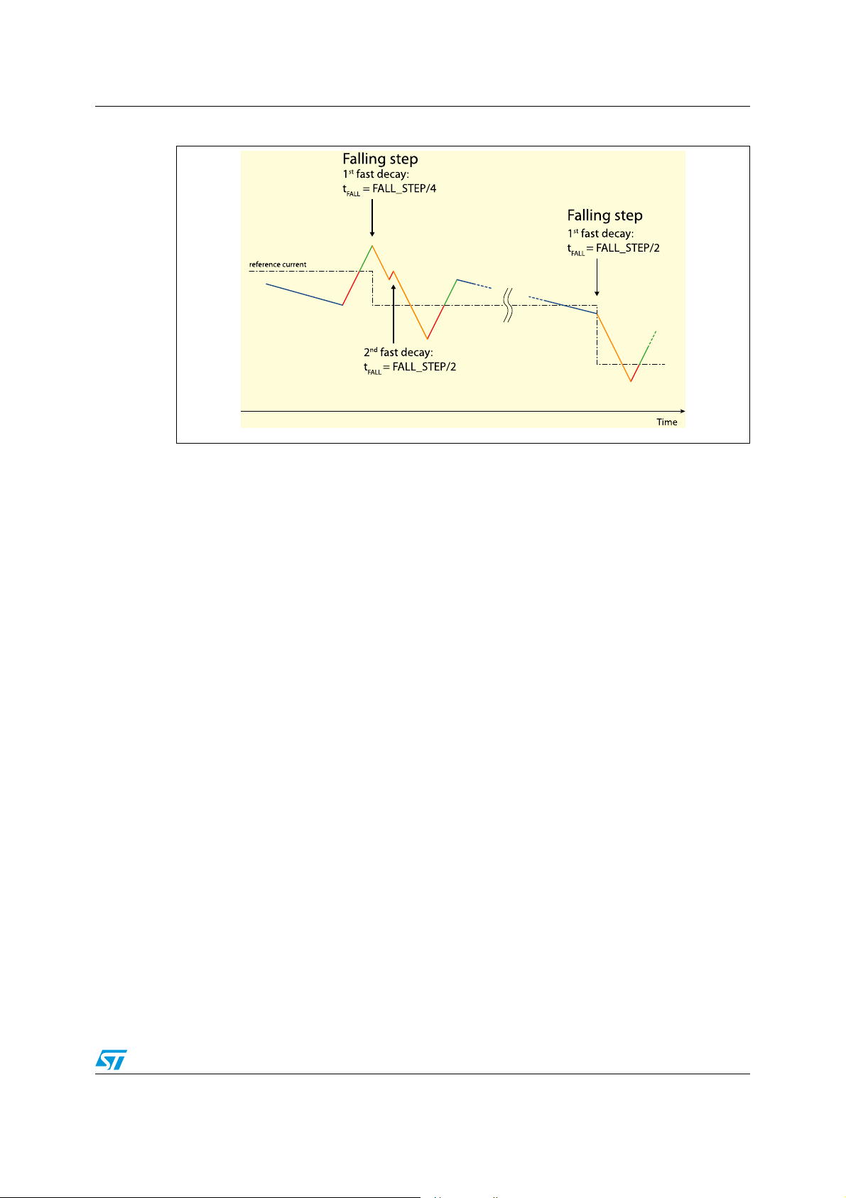
When the target current is decreased by a microstep change (falling step), the device
performs a fast decay in order to reach the new value as fast as possible. Anyway,
exceeding the fast duration may cause a strong ripple on the step change. The L6472
automatically adjusts these fast decays reducing the current ripple.
At reset, the fast decay value (t
value is doubled every time, within the same falling step, an extra fast decay is necessary to
obtain an ON time greater than TON_MIN. The maximum t
FALL_STEP.
At the next falling step, the system uses the last t
Stopping the motor or reaching the current sinewave zero crossing causes the current
control system to return to the reset state.
36/69 Doc ID 022729 Rev 1
) is set to FALL_STEP/4 (T_FAST register). The t
FAL L
value is equal to
FALL
value of the previous falling step.
FALL
FALL
Page 37
L6472 Phase current control
Figure 19. Fast decay tuning during the falling steps
7.4 Torque regulation (output current amplitude regulation)
The output current amplitude can be regulated in two ways: writing the TVAL_ACC,
TVAL_DEC, TVAL_RUN and TVAL_HOLD registers or varying the ADCIN voltage value.
The EN_TQREG bit (CONFIG register) sets the torque regulation method. If this bit is high,
the ADC_OUT prevalue is used to regulate output current amplitude (see Section 9.1.14).
Otherwise the internal analog-to-digital converter is at the user’s disposal and the output
current amplitude is managed by the TVAL_HOLD, TVAL_RUN, TVAL_ACC and
TVAL_DEC registers (see Section 9.1.10).
The voltage applied to the ADCIN pin is sampled at fS frequency and converted in an NADC
bit digital signal. The analog-to-digital conversion result is available in the ADC_OUT
register.
Doc ID 022729 Rev 1 37/69
Page 38
Serial interface L6472
8 Serial interface
The integrated 8-bit serial peripheral interface (SPI) is used for a synchronous serial
communication between the host microprocessor (always master) and the L6472 (always
slave).
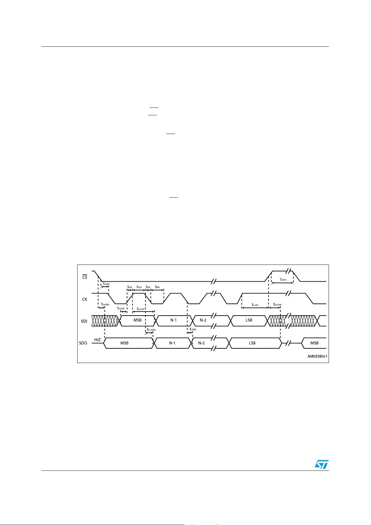
The SPI uses chip select (CS
output (SDO) pins. When CS
(high-impedance).
The communication starts when CS
data communication.
All commands and data bytes are shifted into the device through the SDI input, most
significant bit first. The SDI is sampled on the rising edges of the CK.
All output data bytes are shifted out of the device through the SDO output, most significant
bit first. The SDO is latched on the falling edges of the CK. When a return value from the
device is not available, an all zero byte is sent.
After each byte transmission, the CS
tdisCS in order to allow the device to decode the received command and put the return
value into the shift register.
All timing requirements are shown in Figure 20 (see Section 3 for the respective electrical
characteristics for values).
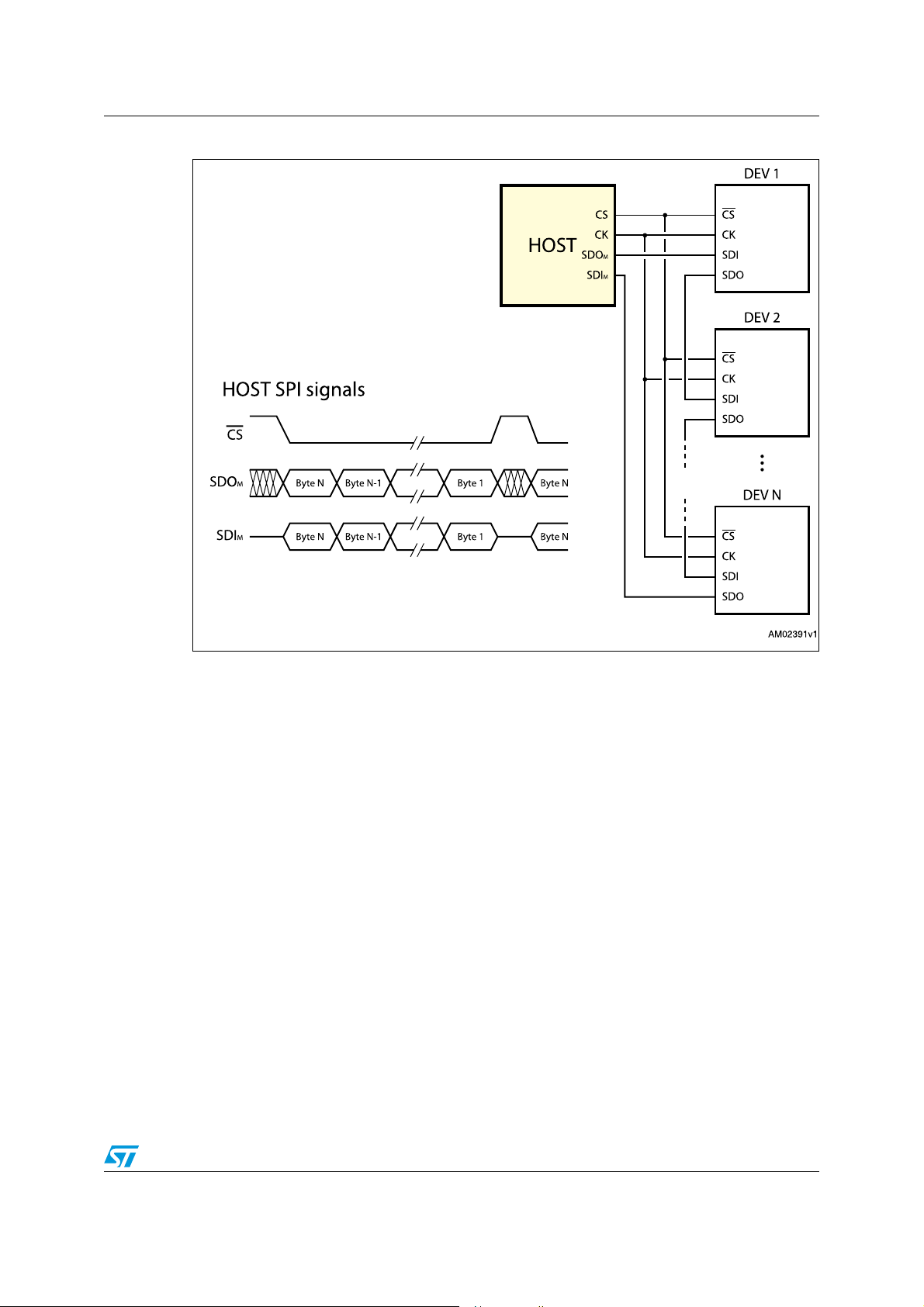
Multiple devices can be connected in a daisy chain configuration, as shown in Figure 21.
Figure 20. SPI timings diagram
), serial clock (CK), serial data input (SDI) and serial data
is high, the device is unselected and the SDO line is inactive
is forced low. The CK line is used for synchronization of
input must be raised and be kept high for at least
38/69 Doc ID 022729 Rev 1
Page 39
L6472 Serial interface
Figure 21. Daisy chain configuration
Doc ID 022729 Rev 1 39/69
Page 40
Programming manual L6472
9 Programming manual
9.1 Register and flag description
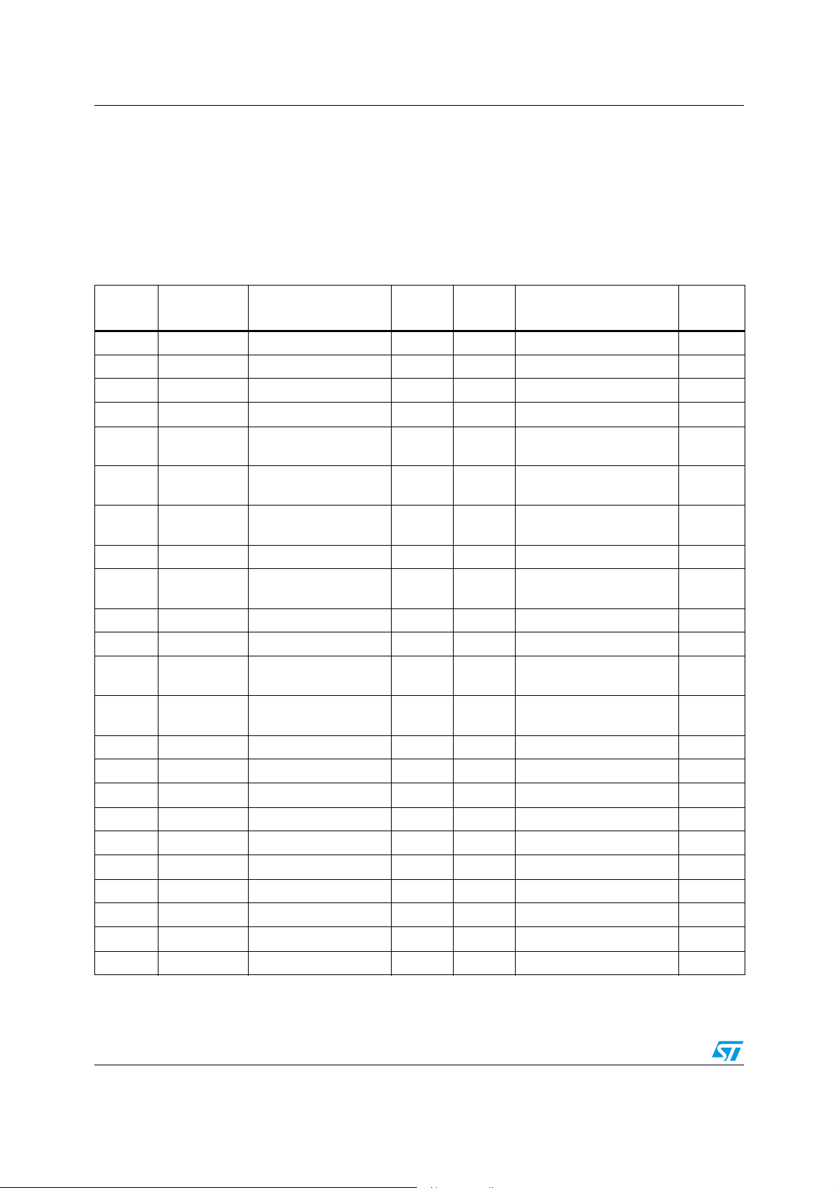
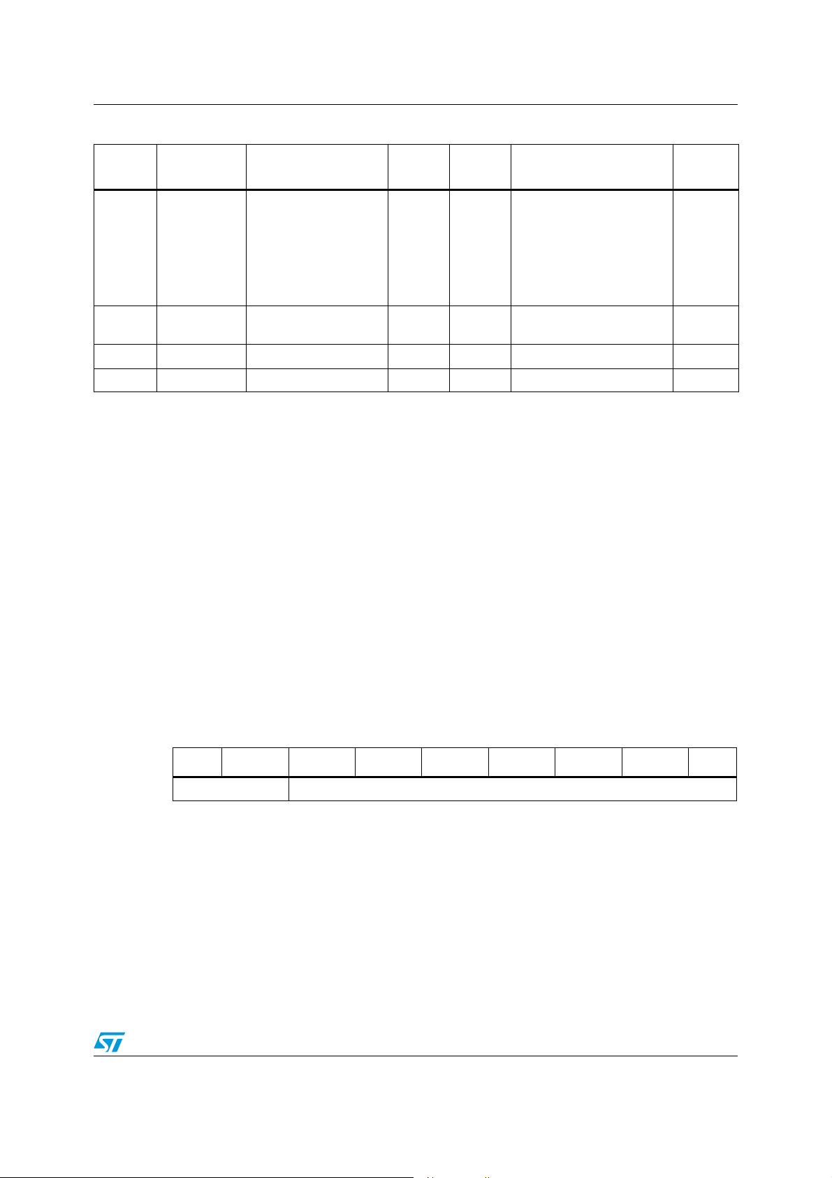
Ta bl e 9 shows a map of the user registers available (detailed description in respective
paragraphs):
Table 9. Register map
Address
[Hex]
Register
name
Register function Len. [bit]
Reset
Hex
Reset Value
Remarks
(1)
h01 ABS_POS Current position 22 000000 0 R, WS
h02 EL_POS Electrical position 9 000 0 R, WS
h03 MARK Mark position 22 000000 0 R, WR
h04 SPEED Current speed 20 00000 0 step/tick (0 step/s) R
h05 ACC Acceleration 12 08A
h06 DEC Deceleration 12 08A
h07 MAX_SPEED Maximum speed 10 041
125.5e-12 step/tick
step/s
125.5e-12 step/tick
step/s
248e-6 step/tick (991.8
step/s)
2
)
2
)
2
(2008
2
(2008
R, WS
R, WS
R, WR
h08 MIN_SPEED Minimum speed 13 000 0 step/tick (0 step/s) R, WS
h15 FS_SPD Full-step speed 10 027
150.7e-6 step/tick (602.7
step/s)
R, WR
h09 TVAL_HOLD Holding current 7 29 1.3125 A R, WR
h0A TVAL_RUN Constant speed current 7 29 1.3125 A R, WR
h0B TVAL_ACC
h0C TVAL_DEC
Acceleration starting
current
Deceleration starting
current
7 29 1.3125 A R, WR
7 29 1.3125 A R, WR
h0D RESERVED Reserved address 16
h0E T_FAST Fast decay/fall step time 8 19 1µs / 5 µs R, WH
h0F TON_MIN Minimum ON time 7 29 20.5 µs R, WH
h10 TOFF_MIN Minimum OFF time 7 29 20.5 µs R, WH
h11 RESERVED Reserved address 8
h12 ADC_OUT ADC output 5 XX
(2)
h13 OCD_TH OCD threshold 4 8 3.38 A R, WR
h14 RESERVED Reserved address 8
h16 STEP_MODE Step mode 8 7 16 microsteps, no synch R, WH
h17 ALARM_EN Alarms enable 8 FF All alarms enabled R, WS
40/69 Doc ID 022729 Rev 1
R
Page 41
L6472 Programming manual
Table 9. Register map (continued)
Address
[Hex]
h18 CONFIG IC configuration 16 2E88
h19 STATUS Status 16 XXXX
h1A RESERVED Reserved address
h1B RESERVED Reserved address
1. R: Readable, WH: writable only when outputs are in high-impedance, WS: writable only when motor is stopped, WR:
always writable.
2. According to startup conditions.
Register
name
Register function Len. [bit]
Reset
Hex
Reset Value
Internal oscillator, 2 MHz
OSCOUT clock, supply
voltage compensation
disabled, overcurrent
shutdown enabled, slew
rate = 290 V/µs TSW =
40 µs
High-impedance state,
(2)
UVLO/reset flag set.
Remarks
9.1.1 ABS_POS
The ABS_POS register contains the current motor absolute position in agreement to the
selected step mode; the stored value unit is equal to the selected step mode (full, half,
quarter, etc.). The value is in 2's complement format and it ranges from -2
At power-on the register is initialized to “0” (HOME position).
21
to +221-1.
(1)
R, WH
R
Any attempt to write the register when the motor is running causes the command to be
ignored and the NOTPERF_CMD flag to rise (see Section 9.1.19).
9.1.2 EL_POS
The EL_POS register contains the current electrical position of the motor. The two MSbits
indicate the current step and the other bits indicate the current microstep (expressed in
step/128) within the step.
Table 10. EL_POS register
Bit 8 Bit 7 Bit 6 Bit 5 Bit 4 Bit 3 Bit 2 Bit 1 Bit 0
STEP MICROSTEP
When the EL_POS register is written by the user the new electrical position is instantly
imposed. When the EL_POS register is written its value must be masked in order to match
with the step mode selected in the STEP_MODE register in order to avoid a wrong
microstep value generation (see Section 9.1.16); otherwise the resulting microstep
sequence is incorrect.
Any attempt to write the register when the motor is running causes the command to be
ignored and the NOTPERF_CMD flag to rise (see Section 9.1.19).
Doc ID 022729 Rev 1 41/69
Page 42

Programming manual L6472
9.1.3 MARK
The MARK register contains an absolute position called MARK, in accordance with the
selected step mode; the stored value unit is equal to the selected step mode (full, half,
quarter, etc.).
It is in 2's complement format and it ranges from -2
21
to +221-1.
9.1.4 SPEED
The SPEED register contains the current motor speed, expressed in step/tick (format
unsigned fixed point 0.28).
In order to convert the SPEED value in step/s the following formula can be used:
Equation 1
tick
28–
⋅
step s⁄[]
SPEED 2
------------- --------------- ------------=
where SPEED is the integer number stored in the register and tick is 250 ns.
The available range is from 0 to 15625 step/s with a resolution of 0.015 step/s.
Note: The range, effectively available to the user, is limited by the MAX_SPEED parameter.
Any attempt to write the register causes the command to be ignored and the
NOTPERF_CMD flag to rise (see Section 9.1.19).
9.1.5 ACC
The ACC register contains the speed profile acceleration expressed in step/tick2 (format
unsigned fixed point 0.40).
In order to convert ACC value in step/s2 the following formula can be used:
Equation 2
where ACC is the integer number stored in the register and tick is 250 ns.
The available range is from 14.55 to 59590 step/s
When the ACC value is set to 0xFFF the device works in infinite acceleration mode.
Any attempt to write to the register when the motor is running causes the command to be
ignored and the NOTPERF_CMD flag to rise (see Section 9.1.19).
9.1.6 DEC
The DEC register contains the speed profile deceleration expressed in step/tick2 (format
unsigned fixed point 0.40).
ACC 2
step s⁄[]
------------ --------------- ----=
40–
⋅
2
tick
2
with a resolution of 14.55 step/s2.
In order to convert the DEC value in step/s2 the following formula can be used:
42/69 Doc ID 022729 Rev 1
Page 43

L6472 Programming manual
Equation 3
step s⁄[]
DEC 2
------------ --------------- ----=
tick
2
40–
⋅
where DEC is the integer number stored in the register and tick is 250 ns.
The available range is from 14.55 to 59590 step/s
2
with a resolution of 14.55 step/s2.
When the device is working in infinite acceleration mode this value is ignored.
Any attempt to write the register when the motor is running causes the command to be
ignored and the NOTPERF_CMD flag to rise (see Section 9.1.19).
9.1.7 MAX_SPEED
The MAX_SPEED register contains the speed profile maximum speed expressed in
step/tick (format unsigned fixed point 0.18).
In order to convert it in step/s the following formula can be used:
Equation 4
step s⁄[]
MAXSPEED 2
------------- -------------- ------------- --------------=
tick
18–
⋅
where MAX_SPEED is the integer number stored in the register and tick is 250 ns.
The available range is from 15.25 to 15610 step/s with a resolution of 15.25 step/s.
9.1.8 MIN_SPEED
The MIN_SPEED register contains the following parameters:
Table 11. MIN_SPEED register
Bit 12 Bit 11 Bit 10 Bit 9 Bit 8 Bit 7 Bit 6 Bit 5 Bit 4 Bit 3 Bit 2 Bit 1 Bit 0
0 MIN_SPEED
The MIN_SPEED parameter contains the speed profile minimum speed. Its value is
expressed in step/tick and to convert it in step/s the following formula can be used:
Equation 5
where MIN_SPEED is the integer number stored in the register and tick is the ramp 250 ns.
The available range is from 0 to 976.3 step/s with a resolution of 0.238 step/s.
Any attempt to write the register when the motor is running causes the NOTPERF_CMD flag
to rise.
step s⁄[]
MINSPEED 2
----------- --------------- ------------- -------------=
tick
24–
⋅
Doc ID 022729 Rev 1 43/69
Page 44
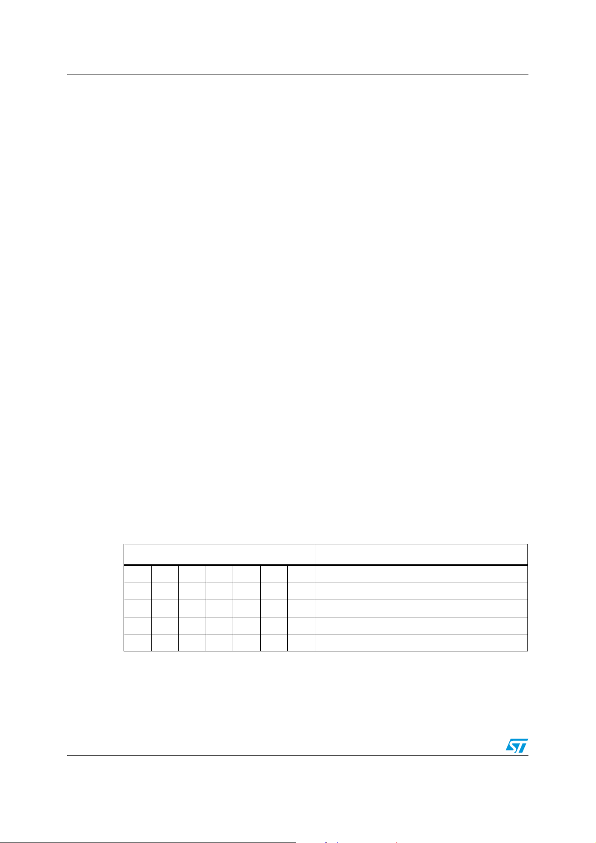
Programming manual L6472
9.1.9 FS_SPD
The FS_SPD register contains the threshold speed. When the actual speed exceeds this
value the step mode is automatically switched to full-step two-phase on. Its value is
expressed in step/tick (format unsigned fixed point 0.18) and to convert it in step/s the
following formula can be used.
Equation 6
step s⁄[]
FSSPD 0.5+()2
------------- --------------- ------------- --------------- ---=
tick
18–
⋅
If the FS_SPD value is set to hFF (max.) the system always works in microstepping mode
(SPEED must go beyond the threshold to switch to full-step mode). Setting FS_SPD to zero
does not have the same effect as setting step mode to full-step two phase on: the zero
FS_SPD value is equivalent to a speed threshold of about 7.63 step/s.
The available range is from 7.63 to 15625 step/s with a resolution of 15.25 step/s.
9.1.10 TVAL_HOLD, TVAL_RUN, TVAL_ACC and TVAL_DEC
The TVAL_HOLD register contains the current value that is assigned to the torque
regulation DAC when the motor is stopped.
The TVAL_RUN register contains the current value that is assigned to the torque regulation
DAC when the motor is running at constant speed.
The TVAL_ACC register contains the current value that is assigned to the torque regulation
DAC during acceleration.
The TVAL_DEC register contains the current value that is assigned to the torque regulation
DAC during deceleration.
The available range is from 31.25 mA to 4 A with a resolution of 31.25 mA, as shown in
Ta bl e 12 .
Table 12. Torque regulation by TVAL_HOLD, TVAL_ACC, TVAL_DEC and
TVAL_RUN registers
TVAL_X [6..0] Output current amplitude
0 0 0 0 0 0 0 31.25 mA
0 0 0 0 0 0 1 62.5 mA
…
…
…
…
…
…
…
1 1 1 1 1 1 0 3.969 A
1 1 1 1 1 1 1 4 A
44/69 Doc ID 022729 Rev 1
…
Page 45
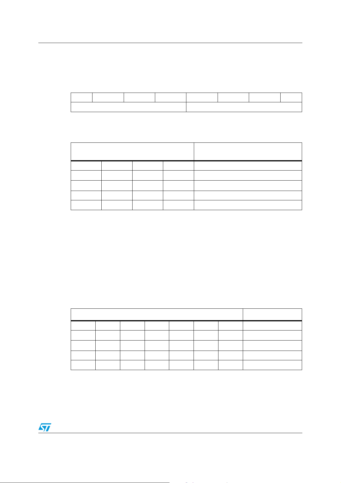
L6472 Programming manual
9.1.11 T_FAST
The T_FAST register contains the maximum fast decay time (TOFF_FAST) and the
maximum fall step time (FALL_STEP) used by the current control system (see Section 7.2
and 7.3 for details):
Bit 7 Bit 6 Bit 5 Bit 4 Bit 3 Bit 2 Bit 1 Bit 0
TOFF_FAST FAST_STEP
The available range for both parameters is from 0.5 µs to 8 µs.
Table 13. Maximum fast decay times
0 0 0 0 0.5 µs
0 0 0 1 1 µs
…
1 1 1 0 7.5 µs
1 1 1 1 8 µs
Any attempt to write to the register when the motor is running causes the command to be
ignored and NOTPERF_CMD to rise (see Section 9.1.19).
9.1.12 TON_MIN
This parameter is used by the current control system when current mode operation is
selected.
The TON_MIN register contains the minimum ON time value used by the current control
system (see Section 7.2).
The available range for both parameters is from 0.5 µs to 64 µs.
Table 14. Minimum ON time
TOFF_FAST [3..0]
FAST_STEP[3..0]
…
…
…
Fast decay time
…
Time
0 0 0 0 0 0 0 0.5 µs
0 0 0 0 0 0 1 1 µs
…
1 1 1 1 1 1 0 63.5 µs
1 1 1 1 1 1 1 64 µs
…
…
…
…
…
…
…
Any attempt to write to the register when the motor is running causes the command to be
ignored and the NOTPERF_CMD to rise (see Section 9.1.19).
Doc ID 022729 Rev 1 45/69
Page 46
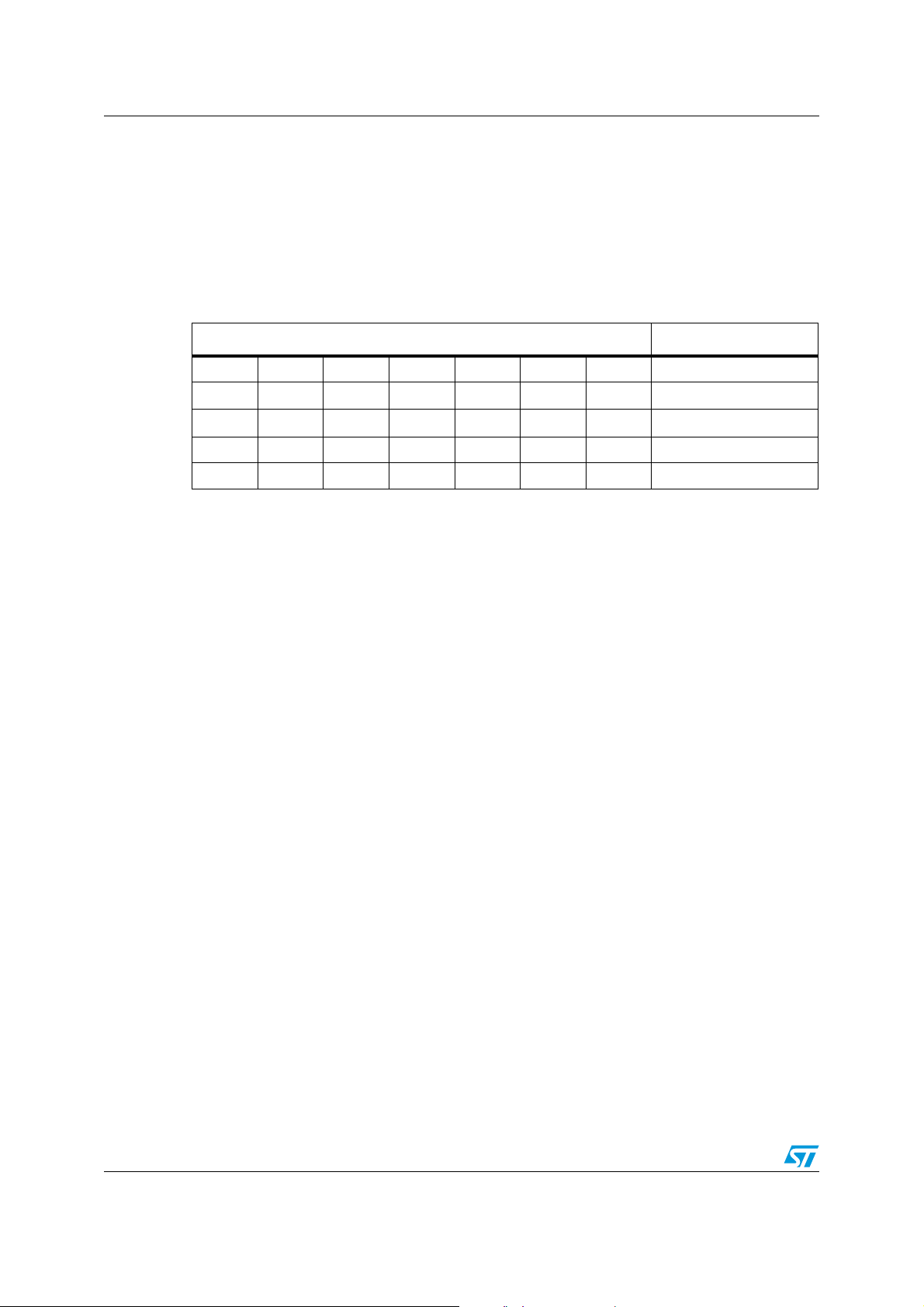
Programming manual L6472
9.1.13 TOFF_MIN
This parameter is used by the current control system when current mode operation is
selected.
The TOFF_MIN register contains the minimum OFF time value used by the current control
system (see Section 7.1 for details).
The available range for both parameters is from 0.5 µs to 64 µs.
Table 15. Minimum OFF time
Time
0 0 0 0 0 0 0 0.5 µs
0 0 0 0 0 0 1 1 µs
…
1 1 1 1 1 1 0 63.5 µs
1 1 1 1 1 1 1 64 µs
Any attempt to write to the register when the motor is running causes the command to be
ignored and NOTPERF_CMD to rise (see Section 9.1.19).
…
…
…
…
…
…
…
46/69 Doc ID 022729 Rev 1
Page 47
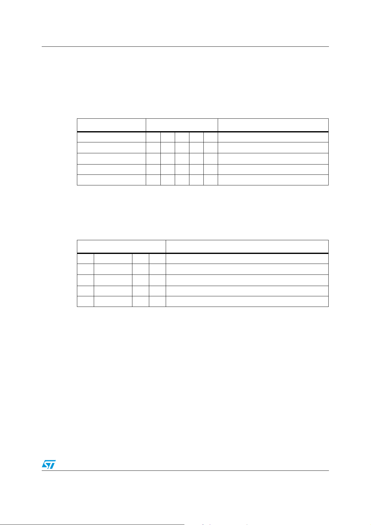
L6472 Programming manual
9.1.14 ADC_OUT
The ADC_OUT register contains the result of the analog-to-digital conversion of the ADCIN
pin voltage.
Any attempt to write to the register causes the command to be ignored and the
NOTPERF_CMD flag to rise (see Section 9.1.19).
Table 16. ADC_OUT value and torque regulation feature
VADCIN/ VREG ADC_OUT [4..0] Output current amplitude
0 0 0 0 0 0 125 mA
1/32 0 0 0 0 1 250 mA
…
30/32 1 1 1 1 0 3.875 A
31/32 1 1 1 1 1 4 A
…
…
…
…
…
…
9.1.15 OCD_TH
The OCD_TH register contains the overcurrent threshold value (see Section 6.9 for details).
The available range is from 375 mA to 6 A, steps of 375 mA, as shown in Ta bl e 1 7 .
Table 17. Overcurrent detection threshold
OCD_TH [3..0] Overcurrent detection threshold
0 0 0 0 375 mA
0 0 0 1 750 mA
…
1 1 1 0 5.625 A
1 1 1 1 6 A
…
…
…
…
Doc ID 022729 Rev 1 47/69
Page 48
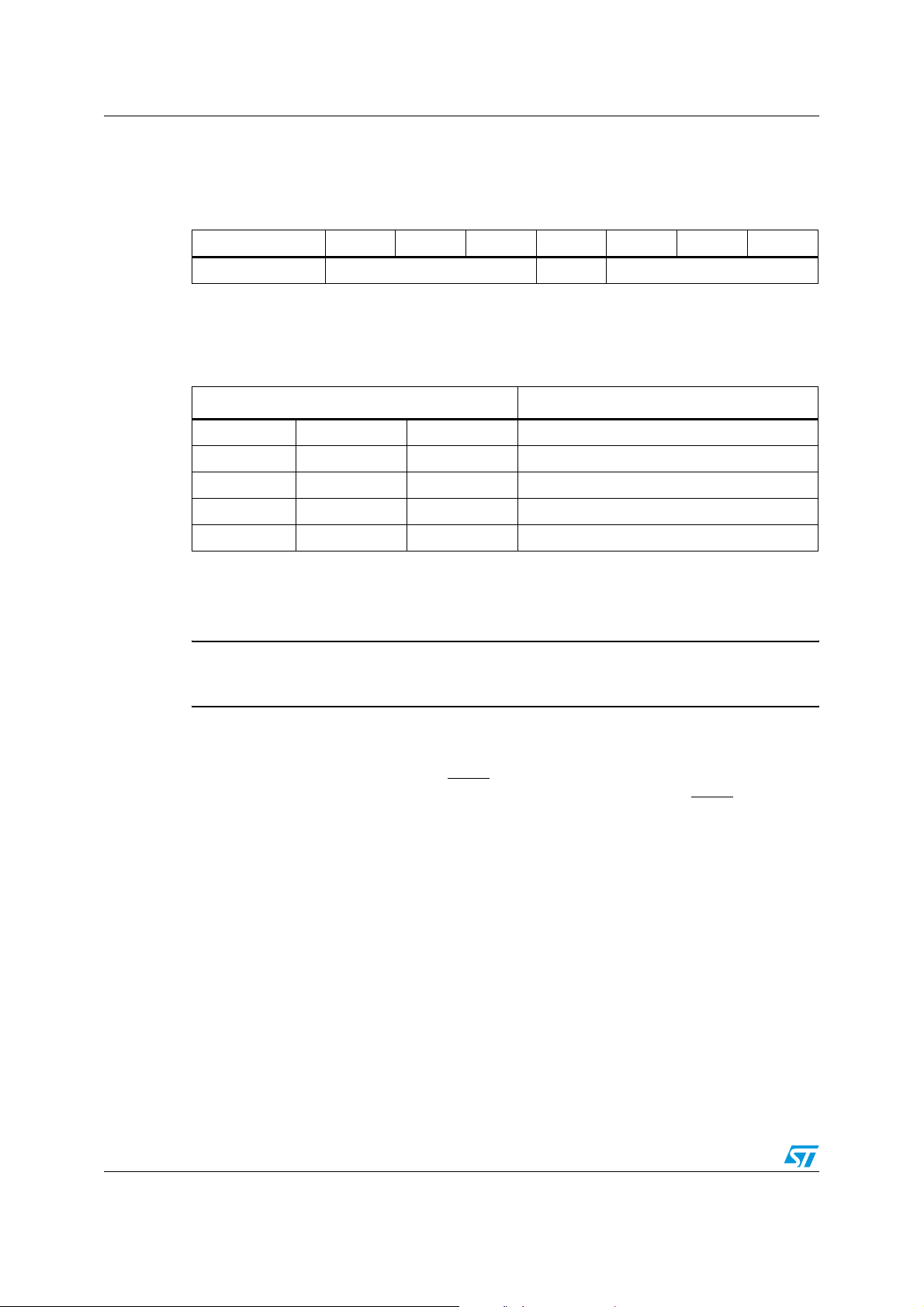
Programming manual L6472
9.1.16 STEP_MODE
The STEP_MODE register has the following structure:
Table 18. STEP_MODE register
Bit 7 Bit 6 Bit 5 Bit 4 Bit 3 Bit 2 Bit 1 Bit 0
SYNC_EN SYNC_SEL 1
1. When the register is written this bit should be set to 1.
The STEP_SEL parameter selects one of five possible stepping modes:
Table 19. Step mode selection
STEP_SEL[2..0] Step mode
0 0 0 Full-step
0 0 1 Half-step
0 1 0 1/4 microstep
0 1 1 1/8 microstep
1 X X 1/16 microstep
(1)
STEP_SEL
Every time the step mode is changed, the electrical position (i.e. the point of microstepping
sinewave that is generated) is reset to the first microstep.
Warning: Every time STEP_SEL is changed the value in the ABS_POS
register looses meaning and should be reset.
Any attempt to write the register when the motor is running causes the command to be
ignored and the NOTPERF_CMD flag to rise (see Section 9.1.19).
When when SYNC_EN bit is set low, BUSY
commands execution, otherwise, when the SYNC_EN bit is set high, the BUSY
/SYNC output is forced low during the
/SYNC
output provides a clock signal according to the SYNC_SEL parameter.
48/69 Doc ID 022729 Rev 1
Page 49
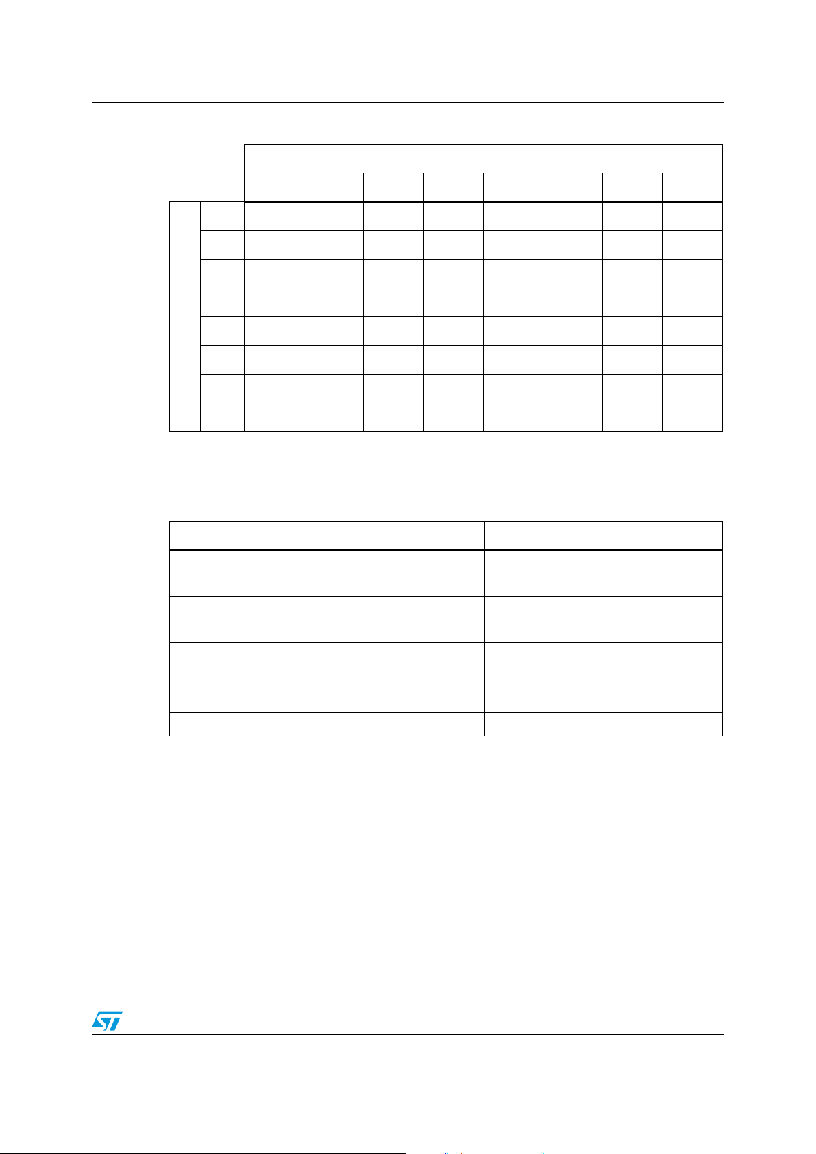
L6472 Programming manual
Table 20. SYNC output frequency
STEP_SEL (fFS is the full-step frequency)
000 001 010 011 100 101 110 111
000 fFS/2 fFS/2 fFS/2 fFS/2 fFS/2 fFS/2 fFS/2 fFS/2
001 NA f
010 NA NA 2· f
011 NA NA NA 4· f
100 NA NA NA NA 8· f
f
FS
FS
fFS f
2· fFS 2· fFS 2· fFS 2· fFS 2· fFS
FS
4· fFS 4· fFS 4· fFS 4· fFS
FS
fFS f
FS
8· fFS 8· fFS 8· fFS
FS
f
FS
SYNC_SEL
101 NA NA NA NA NA NA NA NA
110 NA NA NA NA NA NA NA NA
111 NA NA NA NA NA NA NA NA
The synchronization signal is obtained starting from the electrical position information
(EL_POS register) according to Ta b le 2 1 :
Table 21. SYNC signal source
SYNC_SEL[2..0] Source
0 0 0 EL_POS[7]
0 0 1 EL_POS[6]
0 1 0 EL_POS[5]
0 1 1 EL_POS[4]
FS
1 0 0 EL_POS[3]
1 0 1 UNUSED
1 1 0 UNUSED
1 1 1 UNUSED
1. When this value is selected the BUSY output is forced low.
Doc ID 022729 Rev 1 49/69
(1)
(1)
(1)
Page 50

Programming manual L6472
9.1.17 ALARM_EN
The ALARM_EN register allows the selection of which alarm signals are used to generate
the FLAG output. If the respective bit of the ALARM_EN register is set high, the alarm
condition forces the FLAG pin output down.
Table 22. ALARM_EN register
ALARM_EN bit Alarm condition
0 (LSB) Overcurrent
1 Thermal shutdown
2 Thermal warning
3 Undervoltage
4 UNUSED
5 UNUSED
6 Switch turn-on event
7 (MSB) Wrong or non-performable command
9.1.18 CONFIG
The CONFIG register has the following structure:
Table 23. CONFIG register
Bit 15 Bit 14 Bit 13 Bit 12 Bit 11 Bit 10 Bit 9 Bit 8
PRED_EN TSW POW_SR
Bit 7 Bit 6 Bit 5 Bit 4 Bit 3 Bit 2 Bit 1 Bit 0
OC_SD RESERVED EN_TQREG SW_MODE EXT_CLK OSC_SEL
50/69 Doc ID 022729 Rev 1
Page 51
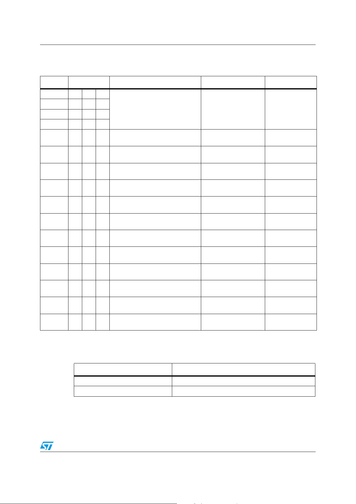
L6472 Programming manual
The OSC_SEL and EXT_CLK bits set the system clock source:
Table 24. Oscillator management
EXT_CLK OSC_SEL[2..0] Clock source OSCIN OSCOUT
0 0 0 0
0 0 0 1
Internal oscillator: 16 MHz Unused Unused
0 0 1 0
0 0 1 1
1 0 0 0 Internal oscillator: 16 MHz Unused
1 0 0 1 Internal oscillator: 16 MHz Unused
1 0 1 0 Internal oscillator: 16 MHz Unused
1 0 1 1 Internal oscillator: 16 MHz Unused
0 1 0 0 External crystal or resonator: 8 MHz Crystal/resonator driving
0 1 0 1
0 1 1 0
0 1 1 1
1 1 0 0
External crystal or resonator:
16 MHz
External crystal or resonator:
24 MHz
External crystal or resonator:
32 MHz
Ext clock source: 8 MHz
(Crystal/resonator driver disabled)
Crystal/resonator driving
Crystal/resonator driving
Crystal/resonator driving
Clock source
Supplies a 2-MHz
clock
Supplies a 4-MHz
clock
Supplies an 8-MHz
clock
Supplies a 16-MHz
clock
Crystal/resonator
driving
Crystal/resonator
driving
Crystal/resonator
driving
Crystal/resonator
driving
Supplies inverted
OSCIN signal
1 1 0 1
1 1 1 0
1 1 1 1
The SW_MODE bit sets the external switch to act as HardStop interrupt or not:
Table 25. External switch hard stop interrupt mode
SW_MODE Switch mode
The OC_SD bit sets if an overcurrent event causes or not the bridges to turn off; the OCD
flag in the STATUS register is forced low anyway:
Ext clock source: 16 MHz
(Crystal/resonator driver disabled)
Ext clock source: 24 MHz
(Crystal/resonator driver disabled)
Ext clock source: 32 MHz
(Crystal/resonator driver disabled)
Clock source
Clock source
Clock source
Supplies inverted
OSCIN signal
Supplies inverted
OSCIN signal
Supplies inverted
OSCIN signal
0 HardStop interrupt
1 User disposal
Doc ID 022729 Rev 1 51/69
Page 52
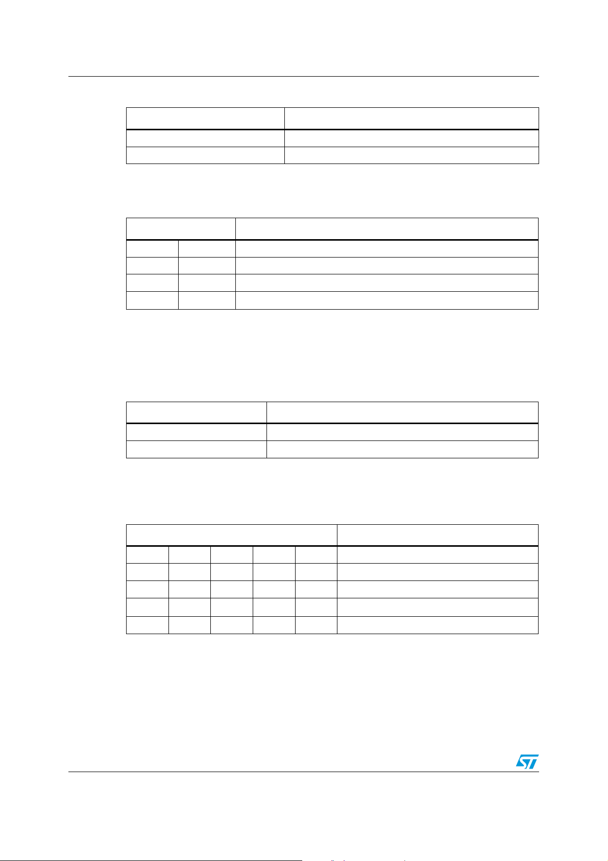
Programming manual L6472
Table 26. Overcurrent event
OC_SD Overcurrent event
1 Bridges shut down
0 Bridges do not shut down
The POW_SR bits set the slew rate value of the power bridge output:
Table 27. Programmable power bridge output slew rate values
POW_SR [1..0] Output Slew rate (1) [V/ìs]
(1)
0 0 180
0 1 180
1 0 290
1 1 530
1. See SRout_r and SRout_f parameters in Table 5 for details.
The TQREG bit sets if the torque regulation (see Section 7.4) is performed through ADCIN
voltage (external) or the TVAL_HOLD, TVAL_ACC, TVAL_DEC and TVAL_RUN registers
(internal):
Table 28. External torque regulation enable
TQREG External torque regulation enable
0 Internal registers
1 ADC input
The TSW parameter is used by the current control system and it sets the target switching
period.
Table 29. Switching period
TSW [4..0] Switching period
0 0 0 0 0 4 µs (250 kHz)
0 0 0 0 1 4 µs (250 kHz)
0 0 0 1 0 8 µs (125 kHz)
…
…
…
…
…
…
1 1 1 1 1 124 µs (8 kHz)
Any attempt to write the CONFIG register when the motor is running causes the command
to be ignored and the NOTPERF_CMD flag to rise (see Section 9.1.19).
52/69 Doc ID 022729 Rev 1
Page 53
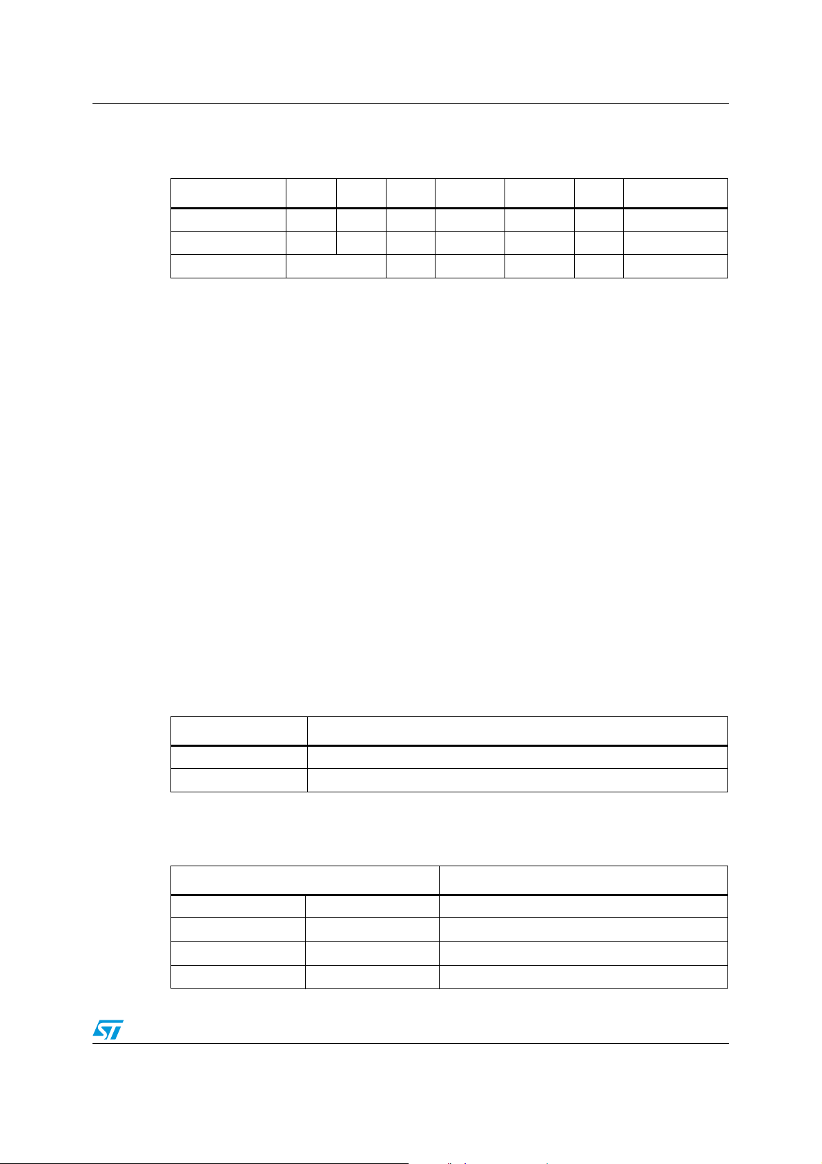
L6472 Programming manual
9.1.19 STATUS
Table 30. STATUS register
Bit 15 Bit 14 Bit 13 Bit 12 Bit 11 Bit 10 Bit 9 Bit 8
SCK_MOD X X OCD TH_SD TH_WRN UVLO WRONG_CMD
Bit 7 Bit 6 Bit 5 Bit 4 Bit 3 Bit 2 Bit 1 Bit 0
NOTPERF_CMD MOT_STATUS DIR SW_EVN SW_F BUSY HiZ
When the HiZ flag is high it indicates that the bridges are in high-impedance state. Any
motion command causes the device to exit from High Z state (HardStop and SoftStop
included), unless error flags forcing a High Z state are active.
The UVLO flag is active low and is set by an undervoltage lockout or reset event (power-up
included). The TH_WRN, TH_SD, OCD flags are active low and indicate respectively
thermal warning, thermal shutdown and overcurrent detection events.
The NOTPERF_CMD and WRONG_CMD flags are active high and indicate, respectively,
that the command received by SPI can't be performed or does not exist at all. The SW_F
reports the SW input status (low for open and high for closed).
The SW_EVN flag is active high and indicates a switch turn-on event (SW input falling
edge).
The UVLO, TH_WRN, TH_SD, OCD, NOTPERF_CMD, WRONG_CMD and SW_EVN flags
are latched: when the respective conditions make them active (low or high) they remain in
that state until a GetStatus command is sent to the IC.
The BUSY bit reflects the BUSY pin status. The BUSY flag is low when a constant speed,
positioning or motion command is under execution and is released (high) after the command
has been completed.
The SCK_MOD bit is an active high flag indicating that the device is working in step-clock
mode. In this case the step-clock signal should be provided through the STCK input pin. The
DIR bit indicates the current motor direction:
Table 31. STATUS register DIR bit
DIR Motor direction
1 Forward
0 Reverse
MOT_STATUS indicates the current motor status:
Table 32. STATUS register MOT_STATE bits
MOT_STATUS Motor status
0 0 Stopped
0 1 Acceleration
1 0 Deceleration
1 1 Constant speed
Doc ID 022729 Rev 1 53/69
Page 54
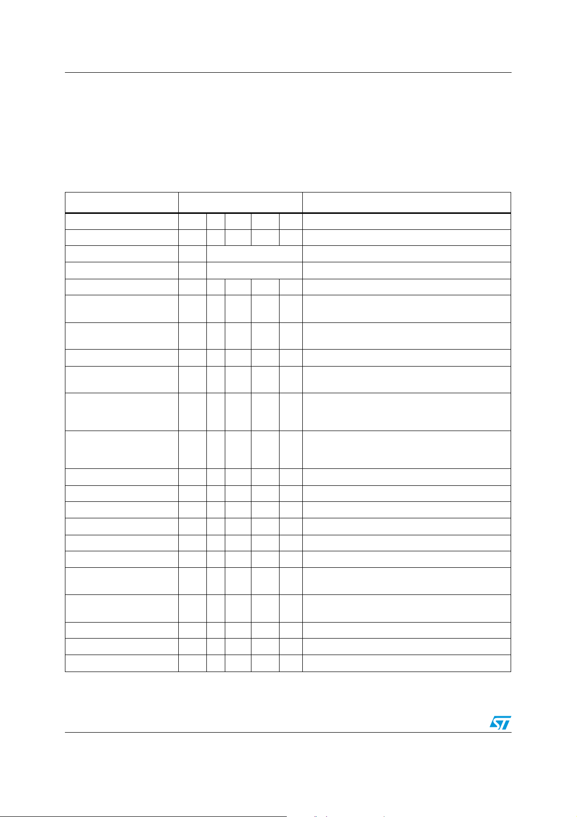
Programming manual L6472
Any attempt to write to the register causes the command to be ignored and the
NOTPERF_CMD to rise (see Section 9.1.19).
9.2 Application commands
A summary of commands is given in Ta b le 3 3 .
Table 33. Application commands
Command Mnemonic Command binary code Action
SetParam(PARAM,VALUE) 000 [PARAM] Writes VALUE in the PARAM register
GetParam(PARAM) 001 [PARAM] Returns the stored value in the PARAM register
[7..5] [4] [3] [2..1] [0]
NOP 000 0 0 00 0 Nothing
Run(DIR,SPD) 010 1 0 00 DIR Sets the target speed and the motor direction
StepClock(DIR) 010 1 1 00 DIR
Move(DIR,N_STEP) 010 0 0 00 DIR
GoTo(ABS_POS) 011 0 0 00 0 Brings motor in ABS_POS position (minimum path)
GoTo_DIR(DIR,ABS_POS) 011 0 1 00 DIR
GoUntil(ACT,DIR,SPD) 100 0 ACT 01 DIR
ReleseSW(ACT, DIR) 100 1 ACT 01 DIR
GoHome 011 1 0 00 0 Brings the motor in HOME position
GoMark 011 1 1 00 0 Brings the motor in MARK position
ResetPos 110 1 1 00 0 Resets the ABS_POS register (set HOME position)
ResetDevice 110 0 0 00 0 Device is reset to power-up conditions.
SoftStop 101 1 0 00 0 Stops motor with a deceleration phase
HardStop 101 1 1 00 0 Stops motor immediately
SoftHiZ 101 0 0 00 0
Puts the device into step-clock mode and imposes
DIR direction
Makes N_STEP (micro) steps in DIR direction (nonperformable when motor is running)
Brings motor in ABS_POS position forcing DIR
direction
Performs a motion in DIR direction with speed SPD
until SW is closed, the ACT action is executed then a
SoftStop takes place
Performs a motion in DIR direction at minimum
speed until the SW is released (open), the ACT
action is executed then a HardStop takes place
Puts the bridges in high-impedance status after a
deceleration phase
HardHiZ 101 0 1 00 0
GetStatus 110 1 0 00 0 Returns the STATUS register value
RESERVED 111 0 1 01 1 RESERVED COMMAND
RESERVED 111 1 1 00 0 RESERVED COMMAND
54/69 Doc ID 022729 Rev 1
Puts the bridges in high-impedance status
immediately
Page 55
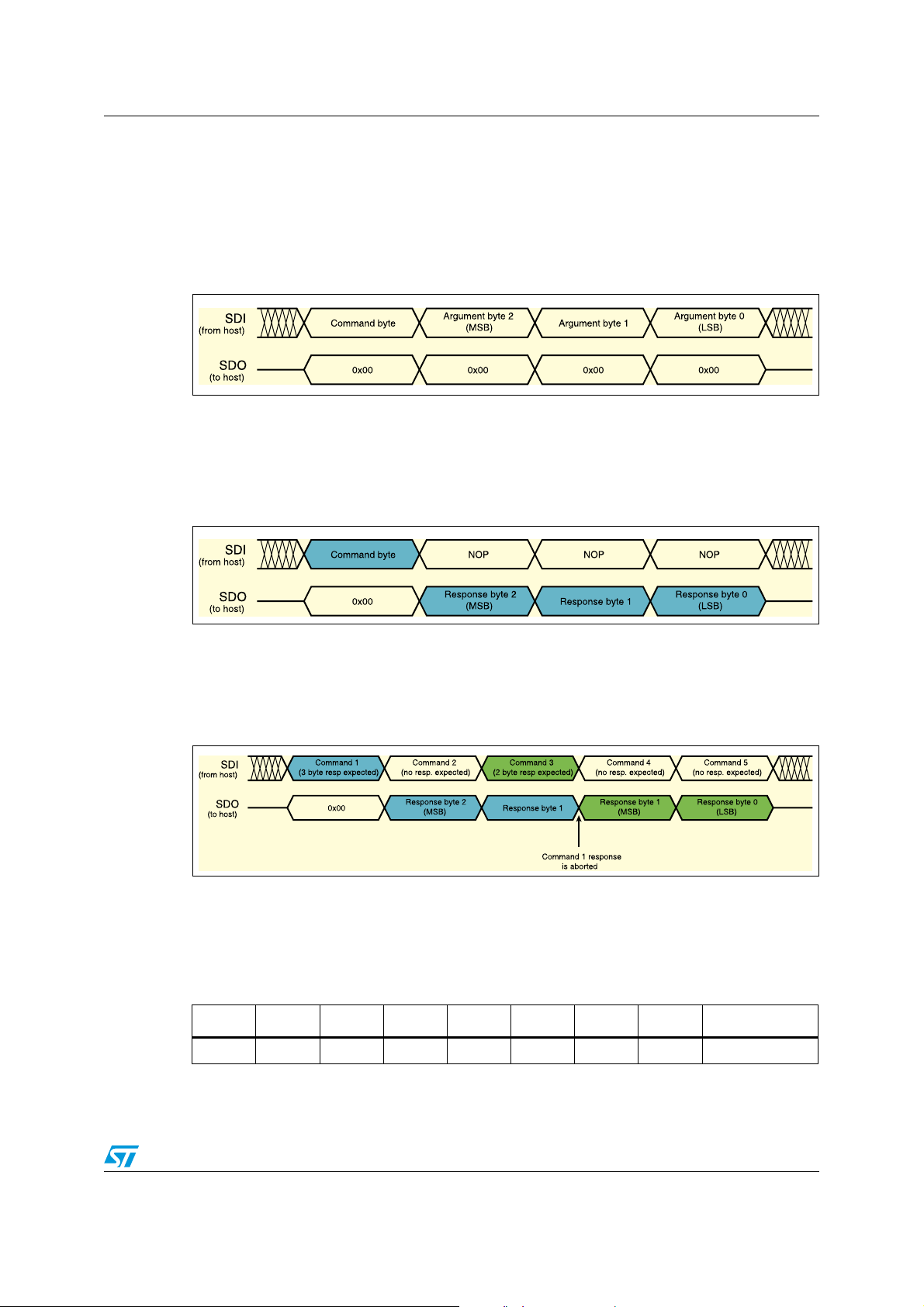
L6472 Programming manual
9.2.1 Command management
The host microcontroller can control motor motion and configure the L6472 through a
complete set of commands.
All commands are composed by a single byte. After the command byte, some argument
bytes should be needed (see Figure 22). Argument length can vary from 1 to 3 bytes.
Figure 22. Command with 3-byte argument
By default the device returns an all zeroes response for any received byte, the only
exceptions are GetParam and GetStatus commands. When one of these commands is
received the following response bytes represents the related register value (see Figure 23).
Response length can vary from 1 to 3 bytes.
Figure 23. Command with 3-byte response
During response transmission, new commands can be sent. If a command requiring a
response is sent before the previous response is completed, the response transmission is
aborted and the new response is loaded into the output communication buffer (see
Figure 24).
Figure 24. Command response aborted
When a byte that does not correspond to a command is sent to the IC, it is ignored and the
WRONG_CMD flag in the STATUS register is raised (see Section 9.1.19).
9.2.2 Nop
Table 34. NOP command structure
Bit 7 Bit 6 Bit 5 Bit 4 Bit 3 Bit 2 Bit 1 Bit 0
0 0 0 0 0 0 0 0 From host
Nothing is performed.
Doc ID 022729 Rev 1 55/69
Page 56
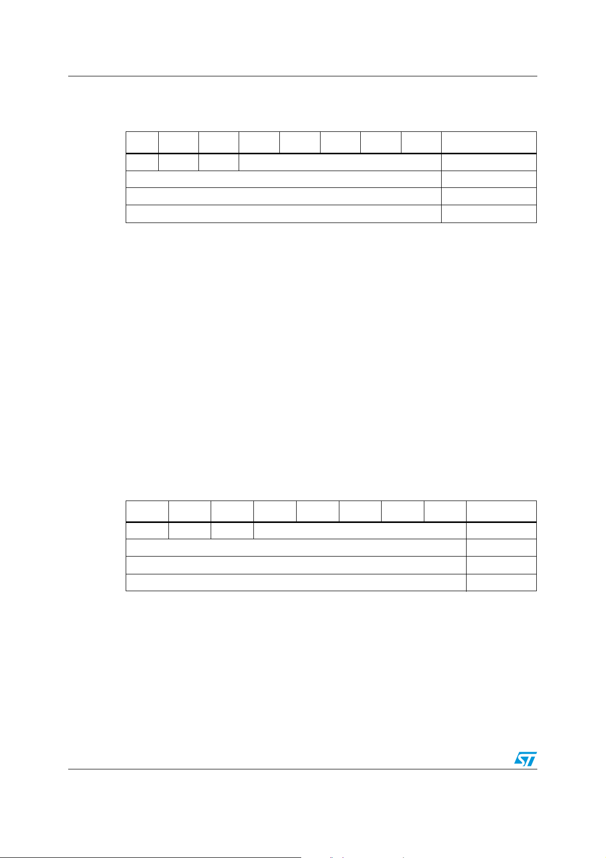
Programming manual L6472
9.2.3 SetParam (PARAM, VALUE)
Table 35. SetParam command structure
Bit 7 Bit 6 Bit 5 Bit 4 Bit 3 Bit 2 Bit 1 Bit 0
0 0 0 PARAM From host
VALUE Byte 2 (if needed)
VALUE Byte 1 (if needed)
VALUE Byte 0
The SetParam command sets the PARAM register value equal to VALUE; PARAM is the
respective register address listed in Ta b le 9 .
The command should be followed by the new register VALUE (most significant byte first).
The number of bytes composing the VALUE argument depends on the length of the target
register (see Ta bl e 9 ).
Some registers cannot be written (see Ta bl e 9 ); any attempt to write one of these registers
causes the command to be ignored and the WRONG_CMD flag to rise at the end of the
command byte as if an unknown command code was sent (see Section 9.1.18).
Some registers can only be written in particular conditions (see Ta b le 9 ); any attempt to
write one of these registers when the conditions are not satisfied causes the command to be
ignored and the NOTPERF_CMD flag to rise at the end of last argument byte (see
Section 9.1.19).
Any attempt to set an inexistent register (wrong address value) causes the command to be
ignored and the WRONG_CMD flag to rise at the end of the command byte as if an
unknown command code was sent.
9.2.4 GetParam (PARAM)
Table 36. GetParam command structure
Bit 7 Bit 6 Bit 5 Bit 4 Bit 3 Bit 2 Bit 1 Bit 0
0 0 1 PARAM From host
This command reads the current PARAM register value; PARAM is the respective register
address listed in Ta bl e 9 .
The command response is the current value of the register (most significant byte first). The
number of bytes composing the command response depends on the length of the target
register (see Ta bl e 9 ).
The returned value is the register one at the moment of GetParam command decoding. If
the register value changes after this moment, the response is not accordingly updated.
ANS Byte 2 (if needed) To host
ANS Byte 1 (if needed) To host
ANS Byte 0 To host
All registers can be read anytime.
56/69 Doc ID 022729 Rev 1
Page 57
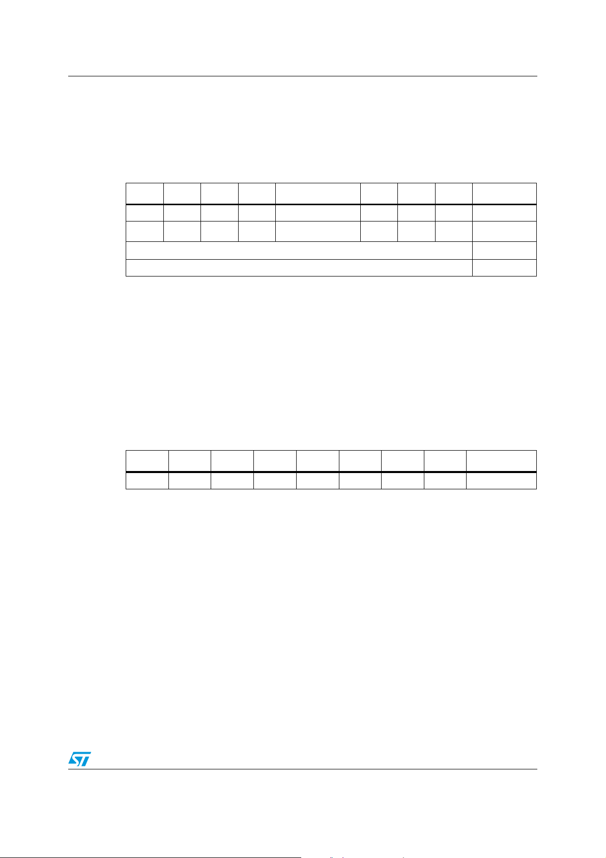
L6472 Programming manual
Any attempt to read an inexistent register (wrong address value) causes the command to be
ignored and WRONG_CMD flag to rise at the end of command byte as if an unknown
command code is sent.
9.2.5 Run (DIR, SPD)
Table 37. Run command structure
Bit 7 Bit 6 Bit 5 Bit 4 Bit 3 Bit 2 Bit 1 Bit 0
0 1 0 1 0 0 0 DIR From host
X X X X SPD (Byte 2) From host
SPD (Byte 1) From host
SPD (Byte 0) From host
The Run command produces a motion at SPD speed; the direction is selected by the DIR
bit: '1' forward or '0' reverse. The SPD value is expressed in step/tick (format unsigned fixed
point 0.28) which is the same format as the SPEED register (see Section 9.1.4).
Note: The SPD value should be lower than MAX_SPEED and greater than MIN_SPEED
otherwise the Run command is executed at MAX_SPEED or MIN_SPEED respectively.
This command keeps the BUSY flag low until the target speed is reached.
This command can be given anytime and is immediately executed.
9.2.6 StepClock (DIR)
Table 38. StepClock command structure
Bit 7 Bit 6 Bit 5 Bit 4 Bit 3 Bit 2 Bit 1 Bit 0
0 1 0 1 1 0 0 DIR From host
The StepClock command switches the device in step-clock mode (see Section 6.7.5) and
imposes the forward (DIR = '1') or reverse (DIR = '0') direction.
When the device is in step-clock mode the SCK_MOD flag in the STATUS register is raised
and the motor is always considered stopped (see Section 6.7.5 and 9.1.18).
The device exits from step-clock mode when a constant speed, absolute positioning or
motion command is sent through SPI. Motion direction is imposed by the respective
StepClock command argument and can by changed by a new StepClock command without
exiting step-clock mode.
Events that cause bridges to be forced into high-impedance state (overtemperature,
overcurrent, etc.) do not cause the device to leave step-clock mode. StepClock command
does not force the BUSY flag low. This command can only be given when the motor is
stopped. If a motion is in progress the motor should be stopped and it is then possible to
send a StepClock command.
Any attempt to perform a StepClock command when the motor is running causes the
command to be ignored and the NOTPERF_CMD flag to rise (see Section 9.1.19).
Doc ID 022729 Rev 1 57/69
Page 58
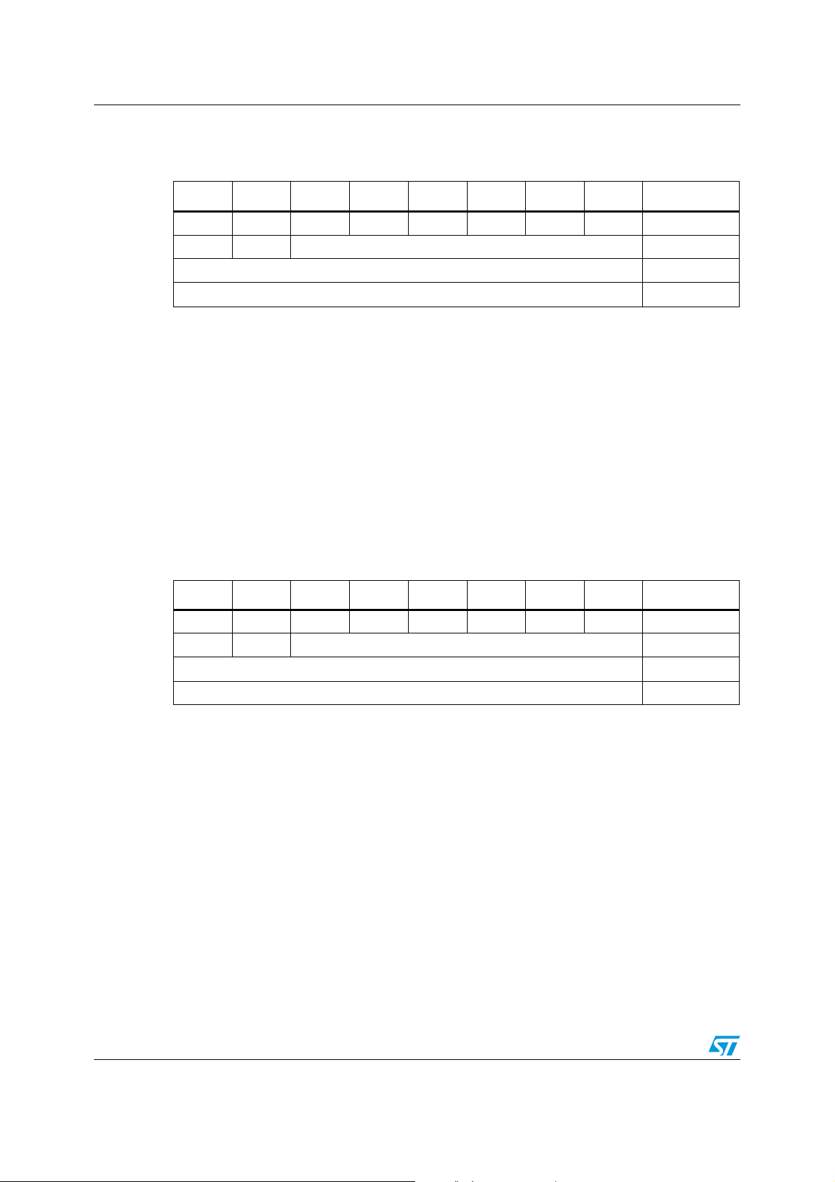
Programming manual L6472
9.2.7 Move (DIR, N_STEP)
Table 39. Move command structure
Bit 7 Bit 6 Bit 5 Bit 4 Bit 3 Bit 2 Bit 1 Bit 0
0 1 0 0 0 0 0 DIR From host
X X N_STEP (Byte 2) From host
N_STEP (Byte 1) From host
N_STEP (Byte 0) From host
The move command produces a motion of N_STEP microsteps; the direction is selected by
the DIR bit ('1' forward or '0' reverse).
The N_STEP value is always in agreement with the selected step mode; the parameter
value unit is equal to the selected step mode (full, half, quarter, etc.).
This command keeps the BUSY flag low until the target number of steps is performed. This
command can only be performed when the motor is stopped. If a motion is in progress the
motor must be stopped and it is then possible to perform a Move command.
Any attempt to perform a Move command when the motor is running causes the command
to be ignored and the NOTPERF_CMD flag to rise (see Section 9.1.19).
9.2.8 GoTo (ABS_POS)
Table 40. GoTo command structure
Bit 7 Bit 6 Bit 5 Bit 4 Bit 3 Bit 2 Bit 1 Bit 0
0 1 1 0 0 0 0 0 From host
X X ABS_POS (Byte 2) From host
The GoTo command produces a motion to the ABS_POS absolute position through the
shortest path. The ABS_POS value is always in agreement with the selected step mode; the
parameter value unit is equal to the selected step mode (full, half, quarter, etc.).
The GoTo command keeps the BUSY flag low until the target position is reached.
This command can be given only when the previous motion command as been completed
(BUSY flag released).
Any attempt to perform a GoTo command when a previous command is under execution
(BUSY low) causes the command to be ignored and the NOTPERF_CMD flag to rise (see
Section 9.1.19).
ABS_POS (Byte 1) From host
ABS_POS (Byte 0) From host
58/69 Doc ID 022729 Rev 1
Page 59

L6472 Programming manual
9.2.9 GoTo_DIR (DIR, ABS_POS)
Table 41. GoTo_DIR command structure
Bit 7 Bit 6 Bit 5 Bit 4 Bit 3 Bit 2 Bit 1 Bit 0
0 1 1 0 1 0 0 DIR From host
X X ABS_POS (Byte 2) From host
ABS_POS (Byte 1) From host
ABS_POS (Byte 0) From host
The GoTo_DIR command produces a motion to the ABS_POS absolute position imposing a
forward (DIR = '1') or a reverse (DIR = '0') rotation. The ABS_POS value is always in
agreement with the selected step mode; the parameter value unit is equal to the selected
step mode (full, half, quarter, etc.).
The GoTo_DIR command keeps the BUSY flag low until the target speed is reached. This
command can be given only when the previous motion command has been completed
(BUSY flag released).
Any attempt to perform a GoTo_DIR command when a previous command is under
execution (BUSY low) causes the command to be ignored and the NOTPERF_CMD flag to
rise (see Section 9.1.19).
9.2.10 GoUntil (ACT, DIR, SPD)
Table 42. GoUntil command structure
Bit 7 Bit 6 Bit 5 Bit 4 Bit 3 Bit 2 Bit 1 Bit 0
1 0 0 0 ACT 0 1 DIR From host
X X X X SPD (Byte 2) From host
The GoUntil command produces a motion at SPD speed imposing a forward (DIR = '1') or a
reverse (DIR = '0') direction. When an external switch turn-on event occurs (see
Section 6.13), the ABS_POS register is reset (if ACT = '0') or the ABS_POS register value is
copied into the MARK register (if ACT = '1'); the system then performs a SoftStop command.
The SPD value is expressed in step/tick (format unsigned fixed point 0.28) which is the
same format as the SPEED register (see Section 9.1.4).
The SPD value should be lower than MAX_SPEED and greater than MIN_SPEED,
otherwise the target speed is imposed at MAX_SPEED or MIN_SPEED respectively.
If the SW_MODE bit of the CONFIG register is set low, the external switch turn-on event
causes a HardStop interrupt instead of the SoftStop one (see Section 6.13 and 9.1.18).
This command keeps the BUSY flag low until the switch turn-on event occurs and the motor
is stopped. This command can be given anytime and is immediately executed.
SPD (Byte 1) From host
SPD (Byte 0) From host
Doc ID 022729 Rev 1 59/69
Page 60
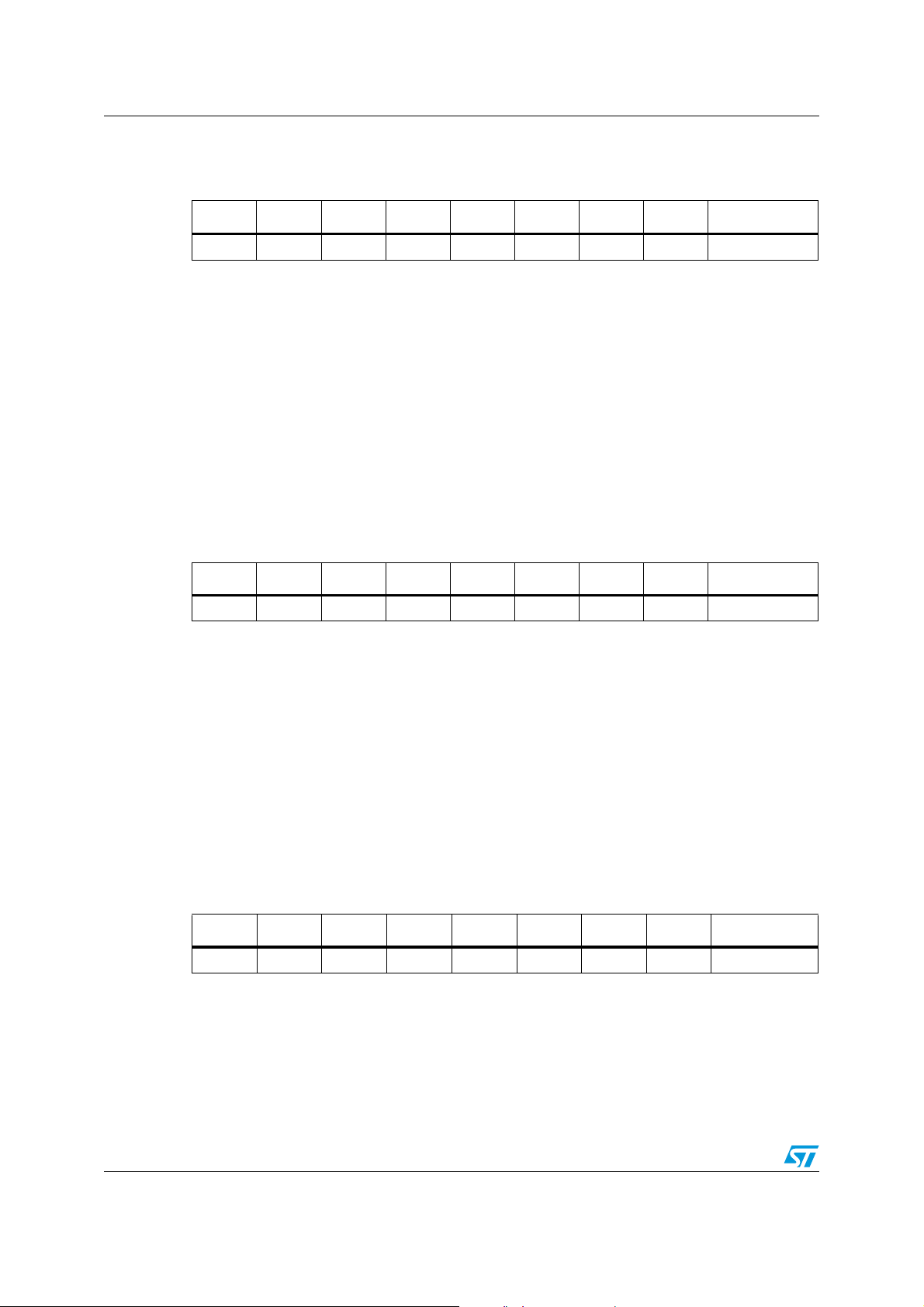
Programming manual L6472
9.2.11 ReleaseSW (ACT, DIR)
Table 43. ReleaseSW command structure
Bit 7 Bit 6 Bit 5 Bit 4 Bit 3 Bit 2 Bit 1 Bit 0
1 0 0 1 ACT 0 1 DIR From host
The ReleaseSW command produces a motion at minimum speed imposing a forward (DIR =
'1') or reverse (DIR = '0') rotation. When SW is released (opened) the ABS_POS register is
reset (ACT = '0') or the ABS_POS register value is copied into the MARK register (ACT =
'1'); the system then performs a HardStop command.
Note that resetting the ABS_POS register is equivalent to setting the HOME position.
If the minimum speed value is less than 5 step/s or low speed optimization is enabled, the
motion is performed at 5 step/s.
The ReleaseSW command keeps the BUSY flag low until the switch input is released and
the motor is stopped.
9.2.12 GoHome
Table 44. GoHome command structure
Bit 7 Bit 6 Bit 5 Bit 4 Bit 3 Bit 2 Bit 1 Bit 0
0 1 1 1 0 0 0 0 From host
The GoHome command produces a motion to the HOME position (zero position) via the
shortest path.
Note that this command is equivalent to the “GoTo(0…0)” command. If a motor direction is
mandatory the GoTo_DIR command must be used (see Section 9.2.9).
The GoHome command keeps the BUSY flag low until the home position is reached. This
command can be given only when the previous motion command has been completed. Any
attempt to perform a GoHome command when a previous command is under execution
(BUSY low) causes the command to be ignored and the NOTPERF_CMD to rise (see
Section 9.1.19).
9.2.13 GoMark
GoMark command structure
Bit 7 Bit 6 Bit 5 Bit 4 Bit 3 Bit 2 Bit 1 Bit 0
0 1 1 1 1 0 0 0 From host
The GoMark command produces a motion to the MARK position performing the minimum
path.
Note that this command is equivalent to the “GoTo (MARK)” command. If a motor direction is
mandatory the GoTo_DIR command must be used.
60/69 Doc ID 022729 Rev 1
Page 61

L6472 Programming manual
The GoMark command keeps the BUSY flag low until the MARK position is reached. This
command can be given only when the previous motion command has been completed
(BUSY flag released).
Any attempt to perform a GoMark command when a previous command is under execution
(BUSY low) causes the command to be ignored and the NOTPERF_CMD flag to rise (see
Section 9.1.19).
9.2.14 ResetPos
Table 45. ResetPos command structure
Bit 7 Bit 6 Bit 5 Bit 4 Bit 3 Bit 2 Bit 1 Bit 0
1 1 0 1 1 0 0 0 From host
The ResetPos command resets the ABS_POS register to zero. The zero position is also
defined as HOME position (see Section 6.5).
9.2.15 ResetDevice
Table 46. ResetDevice command structure
Bit 7 Bit 6 Bit 5 Bit 4 Bit 3 Bit 2 Bit 1 Bit 0
1 1 0 0 0 0 0 0 From host
The ResetDevice command resets the device to power-up conditions (see Section 6.1).
Note: At power-up the power bridges are disabled.
9.2.16 SoftStop
Table 47. SoftStop command structure
Bit 7 Bit 6 Bit 5 Bit 4 Bit 3 Bit 2 Bit 1 Bit 0
1 0 1 1 0 0 0 0 From host
The SoftStop command causes an immediate deceleration to zero speed and a consequent
motor stop; the deceleration value used is the one stored in the DEC register (see
Section 9.1.6).
When the motor is in high-impedance state, a SoftStop command forces the bridges to exit
from high-impedance state; no motion is performed.
This command can be given anytime and is immediately executed. This command keeps
the BUSY flag low until the motor is stopped.
Doc ID 022729 Rev 1 61/69
Page 62
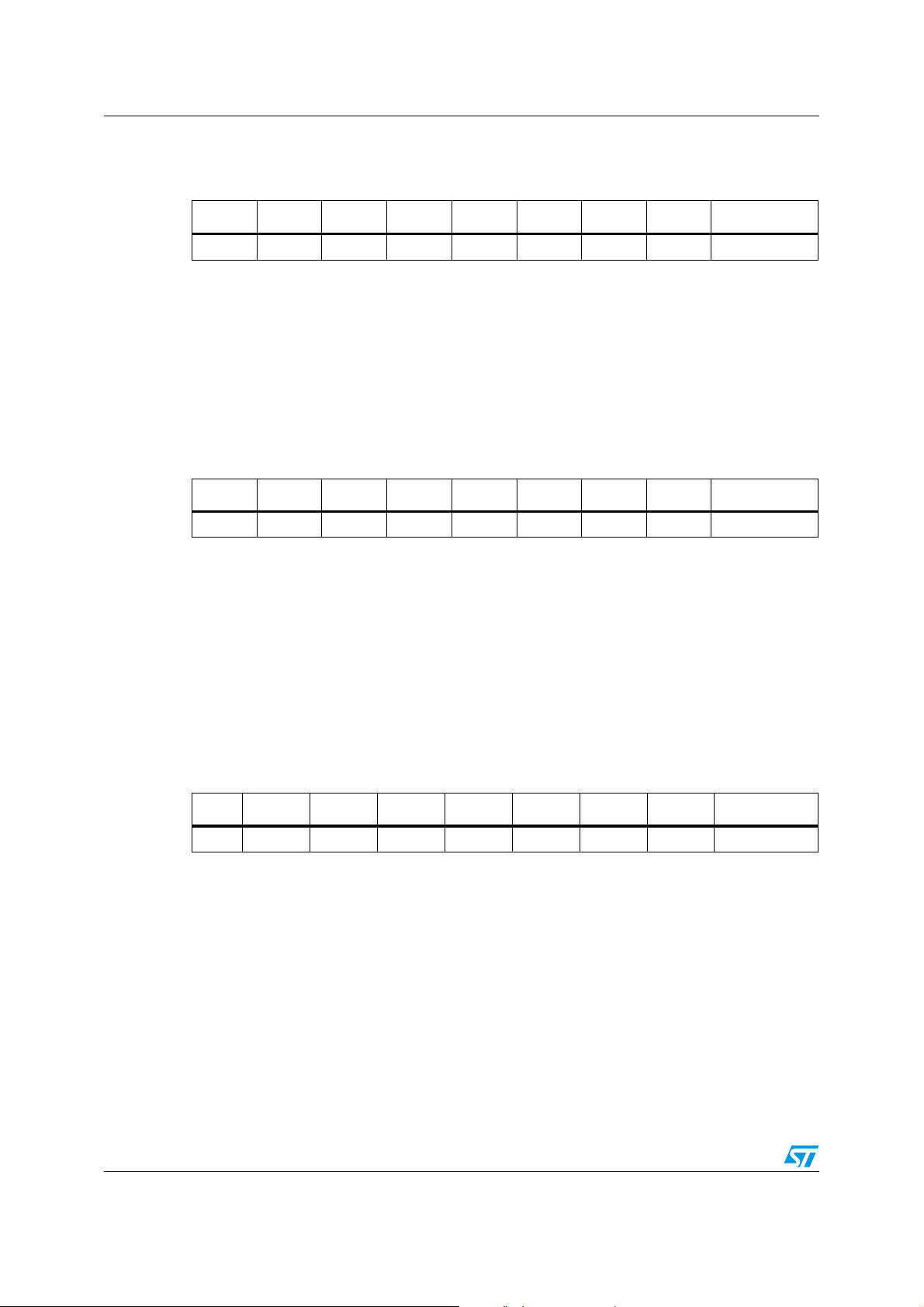
Programming manual L6472
9.2.17 HardStop
Table 48. HardStop command structure
Bit 7 Bit 6 Bit 5 Bit 4 Bit 3 Bit 2 Bit 1 Bit 0
1 0 1 1 1 0 0 0 From host
The HardStop command causes an immediate motor stop with infinite deceleration.
When the motor is in high-impedance state, a HardStop command forces the bridges to exit
from high-impedance state; no motion is performed.
This command can be given anytime and is immediately executed. This command keeps
the BUSY flag low until the motor is stopped.
9.2.18 SoftHiZ
Table 49. SoftHiZ command structure
Bit 7 Bit 6 Bit 5 Bit 4 Bit 3 Bit 2 Bit 1 Bit 0
1 0 1 0 0 0 0 0 From host
The SoftHiZ command disables the power bridges (high-impedance state) after a
deceleration to zero; the deceleration value used is the one stored in the DEC register (see
Section 9.1.6). When bridges are disabled the HiZ flag is raised.
When the motor is stopped, a SoftHiZ command forces the bridges to enter high-impedance
state.
This command can be given anytime and is immediately executed. This command keeps
the BUSY flag low until the motor is stopped.
9.2.19 HardHiZ
Table 50. HardHiZ command structure
Bit 7 Bit 6 Bit 5 Bit 4 Bit 3 Bit 2 Bit 1 Bit 0
1 0 1 0 1 0 0 0 From host
The HardHiZ command immediately disables the power bridges (high-impedance state) and
raises the HiZ flag.
When the motor is stopped, a HardHiZ command forces the bridges to enter highimpedance state.
This command can be given anytime and is immediately executed.
This command keeps the BUSY flag low until the motor is stopped.
62/69 Doc ID 022729 Rev 1
Page 63
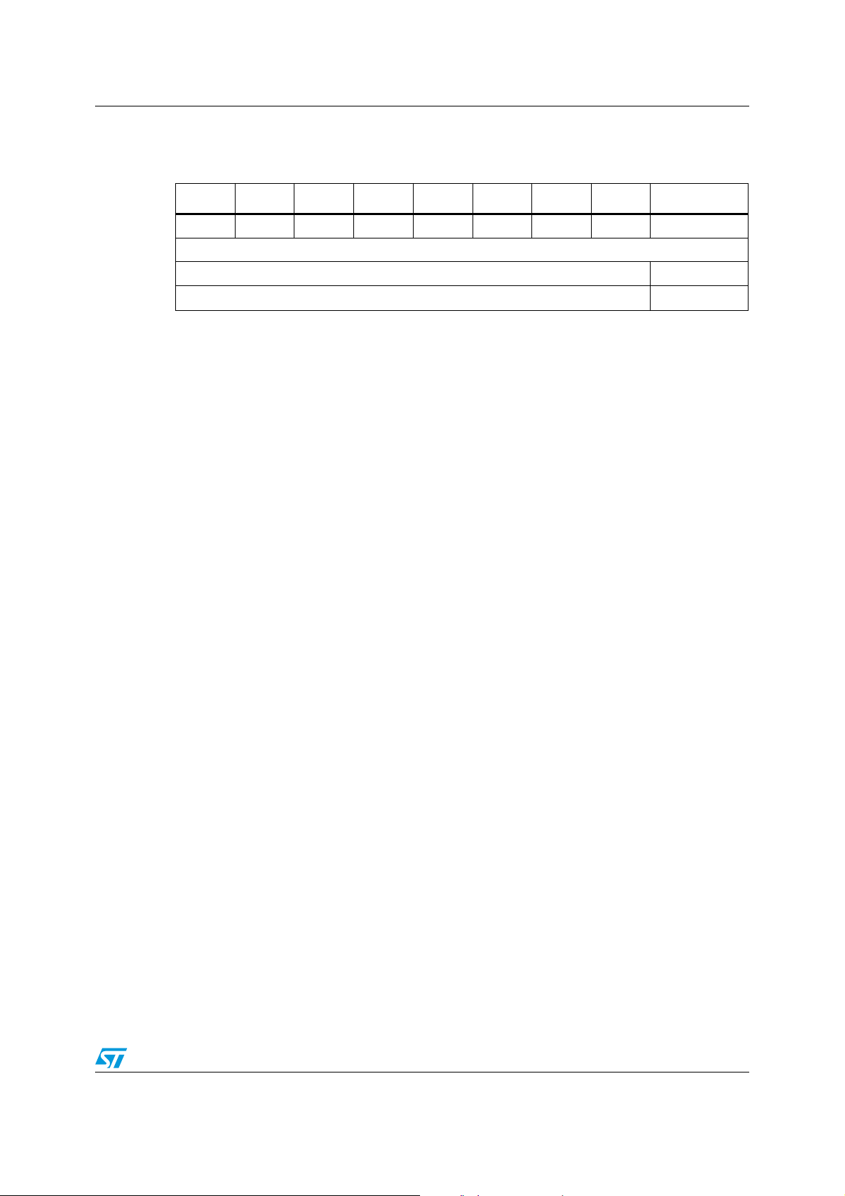
L6472 Programming manual
9.2.20 GetStatus
Table 51. GetStatus command structure
Bit 7 Bit 6 Bit 5 Bit 4 Bit 3 Bit 2 Bit 1 Bit 0
1 1 0 1 0 0 0 0 From host
STATUS MSByte To host
STATUS LSByte To host
The GetStatus command returns the STATUS register value.
The GetStatus command resets the STATUS register warning flags. The command forces
the system to exit from any error state. The GetStatus command does NOT reset the HiZ
flag.
Doc ID 022729 Rev 1 63/69
Page 64
Package mechanical data L6472
10 Package mechanical data
In order to meet environmental requirements, ST offers these devices in different grades of
ECOPACK® packages, depending on their level of environmental compliance. ECOPACK
specifications, grade definitions and product status are available at: www.st.com.
ECOPACK is an ST trademark.
Table 52. HTSSOP28 mechanical data
mm
Dim.
Min. Typ. Max.
A 1.2
A1 0.15
A2 0.8 1.0 1.05
b 0.19 0.3
c 0.09 0.2
(1)
D
D1 5.5
9.6 9.7 9.8
E 6.2 6.4 6.6
(2)
E1
4.3 4.4 4.5
E2 2.8
E 0.65
L 0.45 0.6 0.75
L1 1.0
K 0° 8°
Aaa 0.1
1. Dimension “D” does not include mold flash, protrusions or gate burrs. Mold flash, protrusions or gate burrs
do not exceed 0.15 mm per side.
2. Dimension “E1” does not include interlead flash or protrusions. Interlead flash or protrusions do not exceed
0.25 mm per side.
64/69 Doc ID 022729 Rev 1
Page 65
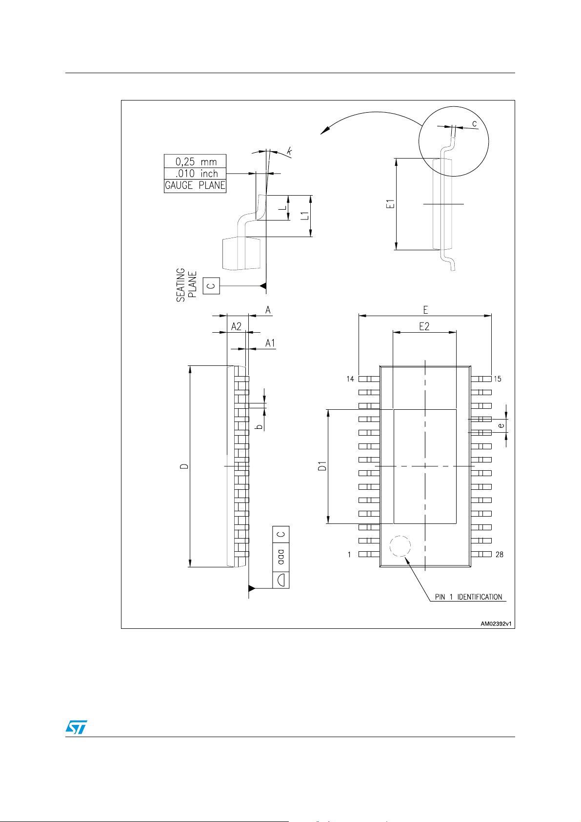
L6472 Package mechanical data
Figure 25. HTSSOP28 mechanical data
Doc ID 022729 Rev 1 65/69
Page 66
Package mechanical data L6472
Table 53. POWERSO36 mechanical data
mm inch
Dim.
Min. Typ. Max. Min. Typ. Max.
A 3.60 0.1417
a1 0.10 0.30 0.003 0.0118
a2 3.30 0.1299
a3 0 0.10 0 0.0039
b 0.22 0.38 0.008 0.0150
c 0.23 0.32 0.009 0.0126
D (1) 15.80 16.00 0.622 0.6299
D1 9.40 9.80 0.370 0.3858
E 13.90 14.50 0.547 0.5709
E1 (1) 10.90 11.10 0.429 0.4370
E2 2.90 0.1142
E3 5.8 6.2 0.228 0.2441
e 0.65 0.025
e3 11.05 0.435
G 0 0.10 0.000 0.0039
H 15.50 15.90 0.610 0.6260
h 1.10 0.0433
L 0.80 1.10 0.031 0.0433
N 10° 10°
S 0° 8° 0° 8°
66/69 Doc ID 022729 Rev 1
Page 67
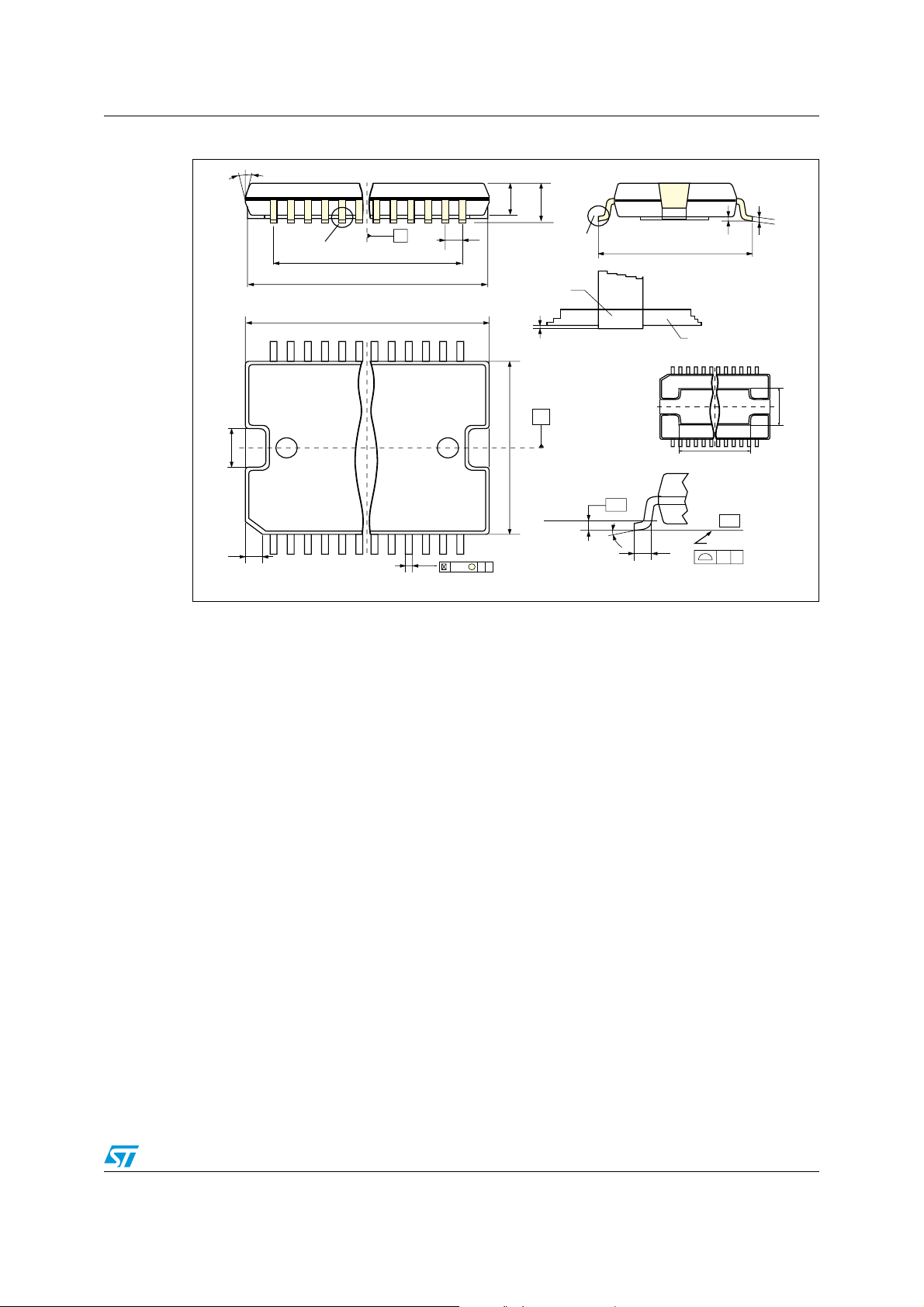
L6472 Package mechanical data
Figure 26. POWERSO36 drawings
11
D
'(7$,/$
$
$
H
'(7$,/%
H
+
OHDG
'(7$,/$
D
(
'
D
VOXJ
F
%277209,(:
%
(
(
'(7$,/%
*DJH3ODQH
6
K[Û
E
0
$%
3620(&
(
'
&
/
6($7,1*3/$1(
*&
&23/$1$5,7<
Doc ID 022729 Rev 1 67/69
Page 68

Revision history L6472
11 Revision history
Table 54. Document revision history
Date Revision Changes
24-Jan-2012 1 Initial release.
68/69 Doc ID 022729 Rev 1
Page 69

L6472
Please Read Carefully:
Information in this document is provided solely in connection with ST products. STMicroelectronics NV and its subsidiaries (“ST”) reserve the
right to make changes, corrections, modifications or improvements, to this document, and the products and services described herein at any
time, without notice.
All ST products are sold pursuant to ST’s terms and conditions of sale.
Purchasers are solely responsible for the choice, selection and use of the ST products and services described herein, and ST assumes no
liability whatsoever relating to the choice, selection or use of the ST products and services described herein.
No license, express or implied, by estoppel or otherwise, to any intellectual property rights is granted under this document. If any part of this
document refers to any third party products or services it shall not be deemed a license grant by ST for the use of such third party products
or services, or any intellectual property contained therein or considered as a warranty covering the use in any manner whatsoever of such
third party products or services or any intellectual property contained therein.
UNLESS OTHERWISE SET FORTH IN ST’S TERMS AND CONDITIONS OF SALE ST DISCLAIMS ANY EXPRESS OR IMPLIED
WARRANTY WITH RESPECT TO THE USE AND/OR SALE OF ST PRODUCTS INCLUDING WITHOUT LIMITATION IMPLIED
WARRANTIES OF MERCHANTABILITY, FITNESS FOR A PARTICULAR PURPOSE (AND THEIR EQUIVALENTS UNDER THE LAWS
OF ANY JURISDICTION), OR INFRINGEMENT OF ANY PATENT, COPYRIGHT OR OTHER INTELLECTUAL PROPERTY RIGHT.
UNLESS EXPRESSLY APPROVED IN WRITING BY TWO AUTHORIZED ST REPRESENTATIVES, ST PRODUCTS ARE NOT
RECOMMENDED, AUTHORIZED OR WARRANTED FOR USE IN MILITARY, AIR CRAFT, SPACE, LIFE SAVING, OR LIFE SUSTAINING
APPLICATIONS, NOR IN PRODUCTS OR SYSTEMS WHERE FAILURE OR MALFUNCTION MAY RESULT IN PERSONAL INJURY,
DEATH, OR SEVERE PROPERTY OR ENVIRONMENTAL DAMAGE. ST PRODUCTS WHICH ARE NOT SPECIFIED AS "AUTOMOTIVE
GRADE" MAY ONLY BE USED IN AUTOMOTIVE APPLICATIONS AT USER’S OWN RISK.
Resale of ST products with provisions different from the statements and/or technical features set forth in this document shall immediately void
any warranty granted by ST for the ST product or service described herein and shall not create or extend in any manner whatsoever, any
liability of ST.
ST and the ST logo are trademarks or registered trademarks of ST in various countries.
Information in this document supersedes and replaces all information previously supplied.
The ST logo is a registered trademark of STMicroelectronics. All other names are the property of their respective owners.
© 2012 STMicroelectronics - All rights reserved
STMicroelectronics group of companies
Australia - Belgium - Brazil - Canada - China - Czech Republic - Finland - France - Germany - Hong Kong - India - Israel - Italy - Japan -
Malaysia - Malta - Morocco - Philippines - Singapore - Spain - Sweden - Switzerland - United Kingdom - United States of America
www.st.com
Doc ID 022729 Rev 1 69/69
 Loading...