

Page 1
L6450
28 CHANNEL INK JET DRIVER
ADVANCE DATA
40VDMOS OUTPUTBREAKDOWN
TWODECODER OPTIONSARE INCLUDED
PRECISEOUTPUTENERGY
ESD OUTPUT PROTECTION WITH CLAMP-
ING DIODES
VERYLOW QUIESCENTCURRENT
PLCC44 OR PQFP44(10 x 10mm)
DESCRIPTION
The L6450 is realized in Multipower BCD Technology which combines isolated DMOS power
transistors with CMOS and Bipolar circuits on the
same IC. By using mixed technology it has been
possible to optimize the logic circuitry and the
powerstage to achieve the best possible performances.
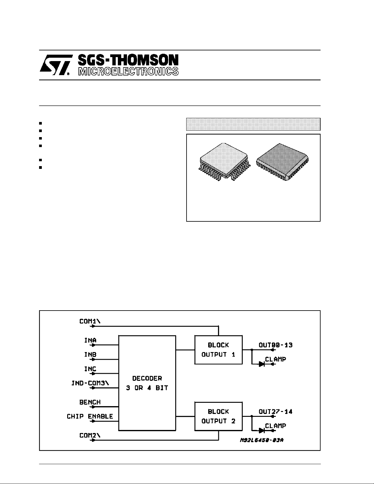
Intended to be used in ink jet Printer Applications
as 4 to 28 (2 x 14) or 3 to 28 (4 x 7) lines selectable decoder/driver, the L6450 device driver has
the advantages of low power CMOS inputs and
logic, with 28 high current and high voltage
DMOS outputs capable of sustaining a maximum
of 40V.
On systempower up the output drivers are locked
out using the chip enable function; four enable in-
MULTIPOWER BCD TECHNOLOGY
PQFP44 PLCC44
puts are available for the differentdriver banks.
An internal power-on system is implemented in
order to avoid wrong output commutation during
the supply voltage transients.
Using a mask option during manufacturing allows
a differentdecoding.
Control of the energy delivered to the print head
ismade by means of a specialcircuitry.
All driver outputs are capable of withdstanding a
contactdischargeof ±8KV with the IC biased.
BLOCK DIAGRAM (case of 4 bit)
March 1994
This is advanced information on a new product now in developmentor undergoing evaluation. Details are subjectto change without notice.
1/9
Page 2
L6450
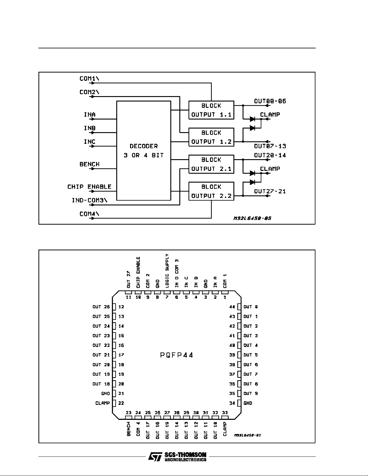
BLOCK DIAGRAM (case of 3 bit)
PQFP44PIN CONNECTION (Top view)
2/9
Page 3
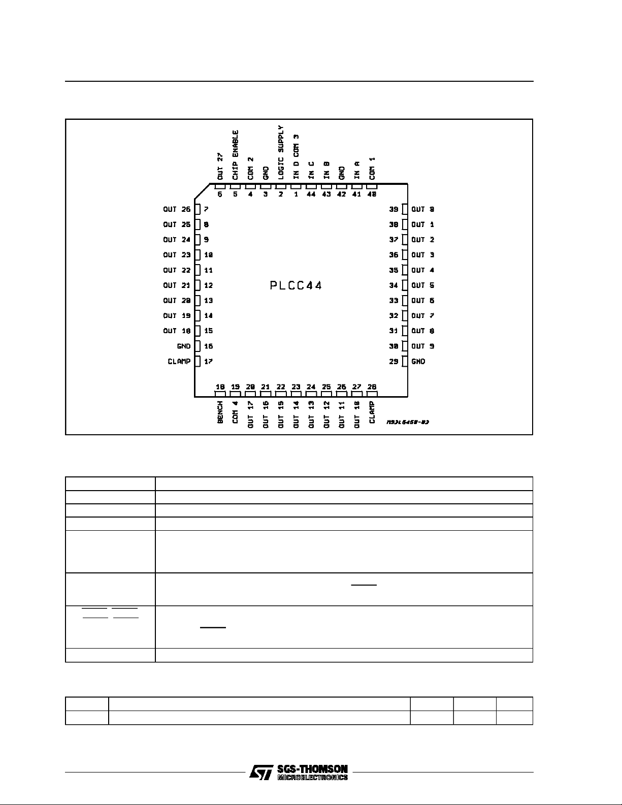
PLCC44PIN CONNECTION (Top view)
L6450
PIN FUNCTIONS
Name Function
V
DD
GND Logic and Power Ground.
OUT0 to OUT27 DMOS Outputs.
CLAMP This pins have to be connected to the power supply voltage of the head resistors, each of the
INA, INB, INC, IND Decoder inputs.
COM1, COM2,
COM3, COM4
CHIP ENABLE A logic high enable the chip.
5V Logic Supply.
output DMOS have their drain connected with the anode of a protection diode, all the catodes
of the protection diodes are collected to the pins clamp. If the CLAMP pins are not connected
to the power, the deviceis not supplied.
The input IND shares the pin with the other input COM3, the two different functions are
selected by the pin Bench.
A low logic input on this pins enable the outputs selected by the decoderinputs according to
the logic level of the pin bench.
The input COM3 shares the pin with the other input IND, the two different functionsare
selected by the pin Bench.
THERMAL DATA
Symbol Parameter PQFP44 PLCC44 Unit
R
th j-amb
(*) device mountedon PCB.
Thermal Resistance Junction-Ambient Max. 55 (*) 65 (*) °C/W
3/9
Page 4

L6450
ABSOLUTE MAXIMUM RATINGS
Symbol Parameter Value Unit
V
V
CLAMP
I
I
PEAK
V
T
T
OUT
OUT
T
DD
V
amb
stg
J
IN
Output Voltage 40 V
Output Clamping Voltage 40 V
Output Continuous Current 0.8 A
Output Peak Current (with duty cycle = 10% TON=4µs) 2 A
JunctionTemperature 150 °C
LogicSupply Voltage 7 V
InputVoltage Range -0.3V to VS+0.3 V
Operating Temperature Range 0 to 70 °C
Storage Temperature Range -55 to 150 °C
D.C. ELECTRICAL CHARACTERISTICS at T
=25°C, VDD=5V,V
amb
=18V( unless otherwisespecified) .
clamp
Symbol Parameter Test Condition Min. Typ. Max. Unit
V
V
CLAMP
V
I
DD
V
IL
IH
I
LL
I
LH
DD
Logic Supply Voltage 4.75 5 5.25 V
Clamping Voltage 9 38 V
Low Level Input Voltage 1.2 V
High Level Input Current VDD-1.2 V
Low Level Input Current VIN=V
High Level Input Current VIN=V
IL
IH
Logic Supply Current (Indipendent from the output
-200 µA
10 µA
5mA
conditions)
V
OUT
∆V
CE
Output Saturation Voltage Tj 25 °C D.C. 0.4A
Tj 25 °C D.C. 0.5A
Tj 90 °C D.C. 0.4A
Tj 90 °C D.C. 0.5A
Output saturation absolute
voltage variationaround the
Tj = 25°Cto90°C D.C.:0.4A
Tj = 25°Cto90°C D.C.:0.5A
0.9
1.1
1.4
1.7
±0.2
±0.25
typ. values for extended
temperature ranges
R
ON 2.2 Ω
DS
A.C. ELECTRICAL CHARACTERISTICS at T
=25°C, VDD=5V.
amb
Symbol Signal Name Parameter Test Condition Min. Typ. Max. Unit
T
S
INA, INB, INC,
SET - UP Time 30 ns
IND Vs COMn
T
H
INA, INB, INC,
HOLD Time 0 ns
IND Vs COMn
T
T
T
∆P
on
off
t
t
wout
r
f
D
COM1,2,3,4
V
OUT 0 to N
S
COM1,2,3,4
V
OUT 0 to N
S
TURN - ON Time I
TURN - OFF Time I
= 0.5A, RL=39Ω
OUT
T
=25to90°C
j
= 0.5A, RL=39Ω
OUT
T
=25to90°C
j
150 ns
150 ns
Rise Time 100 ns
Fall Time 100 ns
Output Pulse Width T
Maximum allowable
variation of the output
= 3.5µsRL=40Ω
win
I
= 0.5A
OUT
R
=39Ω
L
V
= 18V
CLAMP
-20 T
win
+80 ns
±4%
powertransmitted by
eachdriver to the
resistive load
V
V
V
V
V
V
4/9
Page 5

Figure1: Timing Waveforms
L6450
OUTPUTSELECTION
1)Decoder Truth Table when the BENCH =
HIGH;
IND/COM3 = is selected as input decoder ind;
COM1 = a low input enable the OUT0 to
OUT13;
COM2 = A Low Input Enable the OUT14 to
OUT27
IND INC INB
0
0
0
0
0
0
0
0
1
1
1
1
1
1
1
1
0
0
0
0
1
1
1
1
0
0
0
0
1
1
1
1
0
0
1
1
0
0
1
1
0
0
1
1
0
0
1
1
INA
(LSB)
0
1
0
1
0
1
0
1
0
1
0
1
0
1
0
1
OUTPUTS
0.27
1.26
2.25
3.24
4.23
5.22
6.21
7.20
8.19
9.18
10.17
11.16
12.15
13.14
ALL OFF
ALL OFF
2)Decoder Truth Table when the BENCH =
LOW;
IND/COM3= is selected as COM3
COM1: A Low Input Enable the OUT0 to
OUT6
COM2: A Low Input Enable the OUT7 to
OUT13
COM3: A Low Input Enable the OUT14 to
OUT20
COM4: A Low Input Enable the OUT21 to
OUT27
INC INB
0
0
0
0
1
1
1
1
0
0
1
1
0
0
1
1
INA
(LSB)
0
1
0
1
0
1
0
1
OUTPUTS
0, 7,27, 20
1, 8, 26,19
2, 9, 25,18
3, 10, 24, 17
4, 11, 23, 16
5, 12, 22, 15
6, 13, 21, 14
ALL OFF
5/9
Page 6

L6450
Figure2: ApplicationCircuit
6/9
Page 7

PQFP44(14 x 14) PACKAGEMECHANICAL DATA
L6450
DIM.
mm inch
MIN. TYP. MAX. MIN. TYP. MAX.
A 3.40 0.134
A1 0.25 0.0098
A2 2.55 2.80 3.05 0.100 0.110 0.120
B 0.35 0.50 0.0138 0.0197
C 0.13 0.23 0.005 0.009
D 16.95 17.20 17.45 0.667 0.677 0.687
D1 13.90 14.00 14.10 0.547 0.551 0.555
D3 10.00 0.394
e 1.00 0.039
E 16.95 17.20 17.45 0.667 0.677 0.687
E1 13.90 14.00 14.10 0.547 0.551 0.555
E3 10.00 0.394
L 0.65 0.80 0.95 0.025 0.0315 0.0374
L1 1.60 0.063
K 0°(min.), 7°(max.)
D
D1
2333
34
B
44
1
e
11
PQFP44
22
E3D3E1
12
E
L1
L
0.10mm
.004
Seating Plane
K
A1
B
A
A2
C
7/9
Page 8

L6450
PLCC44PACKAGE MECHANICAL DATA
DIM.
MIN. TYP. MAX. MIN. TYP. MAX.
A 17.4 17.65 0.685 0.695
B 16.51 16.65 0.650 0.656
C 3.65 3.7 0.144 0.146
D 4.2 4.57 0.165 0.180
d1 2.59 2.74 0.102 0.108
d2 0.68 0.027
E 14.99 16 0.590 0.630
e 1.27 0.050
e3 12.7 0.500
F 0.46 0.018
F1 0.71 0.028
G 0.101 0.004
M 1.16 0.046
M1 1.14 0.045
mm inch
8/9
Page 9

L6450
Information furnished is believed to be accurate and reliable. However, SGS-THOMSON Microelectronics assumes no responsibility for the
consequences of use of such information nor for any infringement of patents or otherrights of third parties which may result from itsuse. No
license is granted by implication or otherwise under any patent or patent rights of SGS-THOMSON Microelectronics. Specifications mentioned in this publication are subject to change without notice. This publication supersedes and replaces all information previously supplied.
SGS-THOMSON Microelectronics products are not authorized for use as critical components in life support devices or systems without express written approval of SGS-THOMSON Microelectronics.
1994 SGS-THOMSON Microelectronics - All RightsReserved
Australia - Brazil- France - Germany -Hong Kong - Italy - Japan- Korea - Malaysia - Malta - Morocco - The Netherlands - Singapore -
SGS-THOMSON Microelectronics GROUP OF COMPANIES
Spain - Sweden - Switzerland - Taiwan - Thaliand- United Kingdom - U.S.A.
9/9
 Loading...