

Page 1

High-voltage high and low side driver
Features
■ High voltage rail up to 600 V
■ dV/dt immunity ± 50 V/nsec in full temperature
range
■ Driver current capability:
– 290 mA source
– 430 mA sink
■ Switching times 75/35 nsec rise/fall with 1 nF
load
■ 3.3 V, 5 V TTL/CMOS inputs with hysteresis
■ Integrated bootstrap diode
■ Operational amplifier for advanced current
sensing
■ Adjustable dead-time
■ Interlocking function
■ Compact and simplified layout
■ Bill of material reduction
■ Flexible, easy and fast design
L6392
SO-14
Description
The L6392 is a high-voltage device manufactured
with the BCD “OFF-LINE” technology. It is a single
chip half-bridge gate driver for N-channel Power
MOSFET or IGBT.
The high side (floating) section is designed to
stand a voltage rail up to 600 V. The logic inputs
are CMOS/TTL compatible down to 3.3 V for easy
interfacing microcontroller/DSP
The IC embeds an operational amplifier suitable
for advanced current sensing in applications such
as field oriented motor control.
DIP-14
Applications
■ Motor driver for home appliances, factory
automation, industrial drives.
■ HID ballasts, power supply units.
Table 1. Device summary
Order codes Package Packaging
L6392N DIP-14 Tube
L6392D SO-14 Tube
L6392DTR SO-14 Tape and reel
August 2010 Doc ID 14494 Rev 5 1/20
www.st.com
20
Page 2

Contents L6392
Contents
1 Block diagram . . . . . . . . . . . . . . . . . . . . . . . . . . . . . . . . . . . . . . . . . . . . . . 3
2 Pin connection . . . . . . . . . . . . . . . . . . . . . . . . . . . . . . . . . . . . . . . . . . . . . . 4
3 Truth table . . . . . . . . . . . . . . . . . . . . . . . . . . . . . . . . . . . . . . . . . . . . . . . . . 5
4 Electrical data . . . . . . . . . . . . . . . . . . . . . . . . . . . . . . . . . . . . . . . . . . . . . . 6
4.1 Absolute maximum ratings . . . . . . . . . . . . . . . . . . . . . . . . . . . . . . . . . . . . . 6
4.2 Thermal data . . . . . . . . . . . . . . . . . . . . . . . . . . . . . . . . . . . . . . . . . . . . . . . 6
4.3 Recommended operating conditions . . . . . . . . . . . . . . . . . . . . . . . . . . . . . 7
5 Electrical characteristics . . . . . . . . . . . . . . . . . . . . . . . . . . . . . . . . . . . . . 8
5.1 AC operation . . . . . . . . . . . . . . . . . . . . . . . . . . . . . . . . . . . . . . . . . . . . . . . 8
5.2 DC operation . . . . . . . . . . . . . . . . . . . . . . . . . . . . . . . . . . . . . . . . . . . . . . 10
6 Waveforms definitions . . . . . . . . . . . . . . . . . . . . . . . . . . . . . . . . . . . . . . 13
7 Typical application diagram . . . . . . . . . . . . . . . . . . . . . . . . . . . . . . . . . . 14
8 Bootstrap driver . . . . . . . . . . . . . . . . . . . . . . . . . . . . . . . . . . . . . . . . . . . 15
8.1 CBOOT selection and charging . . . . . . . . . . . . . . . . . . . . . . . . . . . . . . . . 15
9 Package mechanical data . . . . . . . . . . . . . . . . . . . . . . . . . . . . . . . . . . . . 17
10 Revision history . . . . . . . . . . . . . . . . . . . . . . . . . . . . . . . . . . . . . . . . . . . 19
2/20 Doc ID 14494 Rev 5
Page 3

L6392 Block diagram
1 Block diagram
Figure 1. Block diagram
HIN
LIN
GND
OPOUT
from LVG
BOOTSTRAP DRIVER
LOGIC
SHOOT
THROUGH
PREVENTION
DEAD
TIME
V
CC
4
UV
DETECTION
3
5V
1
SD
2
7
DT
5
6
FLOATING STRUCTURE
UV
DETECTION
LEVEL
SHIFTER
S
R
OPAMP
BOOT
14
HVG
DRIVER
V
CC
DRIVER
V
CC
+
-
LVG
HVG
13
OUT
12
LVG
10
OP+
8
OP-
9
Doc ID 14494 Rev 5 3/20
Page 4

Pin connection L6392
T
2 Pin connection
Figure 2. Pins connection (top view)
LIN
SD
HIN
VCC
DT
OPOUT
GND
1
2
3
4
5
6
7
14
13
12
11
10
BOO
HVG
OUT
NC
LVG
9
OP-
8
OP+
Table 2. Pin description
Pin N# Pin name Type Function
1LIN
(1)
2SD
3 HIN I High side driver logic input (active high)
4 VCC P Lower section supply voltage
5 DT I Dead time setting
6 OPOUT O Opamp output
7 GND P Ground
8 OP+ I Opamp non inverting input
I Low side driver logic input (active low)
I Shut down logic input (active low)
9 OP- I Opamp inverting input
10 LVG
(1)
O Low side driver output
11 NC Not connected
12 OUT P High side (floating) common voltage
13 HVG
(1)
O High side driver output
14 BOOT P Bootstrapped supply voltage
1. The circuit provides less than 1 V on the LVG and HVG pins (@ Isink = 10 mA), with VCC > 3 V. This allows
to omitting the “bleeder” resistor connected between the gate and the source of the external MOSFET
normally used to hold the pin low; the gate driver assures low impedance also in SD condition.
4/20 Doc ID 14494 Rev 5
Page 5

L6392 Truth table
3 Truth table
Table 3. Truth table
Inputs Outputs
SD
LXXLL
HLLHL
HLHL L
HHL L L
HHHLH
Note: X: don’t care
LIN HIN LVG HVG
Doc ID 14494 Rev 5 5/20
Page 6

Electrical data L6392
4 Electrical data
4.1 Absolute maximum ratings
Table 4. Absolute maximum rating
Value
Symbol Parameter
Min Max
Unit
V
V
V
V
V
V
V
dV
P
T
Supply voltage - 0.3 + 21 V
CC
Output voltage V
out
Bootstrap voltage - 0.3 620 V
boot
High side gate output voltage V
hvg
Low side gate output voltage -0.3 VCC + 0.3 V
Ivg
Opamp non-inverting input -0.3 VCC + 0.3 V
op+
Opamp inverting input -0.3 VCC + 0.3 V
op-
Logic input voltage -0.3 15 V
V
i
/dt Allowed output slew rate 50 V/ns
out
Total power dissipation (TA = 25 °C) 800 mW
tot
Junction temperature 150 °C
T
J
Storage temperature -50 150 °C
stg
-21 V
boot
- 0.3 V
out
+0.3 V
boot
+ 0.3 V
boot
Note: ESD immunity for pins 12, 13 and 14 is guaranteed up to 1 kV (Human body model)
4.2 Thermal data
Table 5. Thermal data
Symbol Parameter SO-14 DIP-14 Unit
R
th(JA)
Thermal resistance junction to ambient 165 100 °C/W
6/20 Doc ID 14494 Rev 5
Page 7

L6392 Electrical data
4.3 Recommended operating conditions
Table 6. Recommended operating conditions
Symbol Pin Parameter Test condition Min Max Unit
V
CC
V
BO
V
out
f
sw
T
J
1. VBO = V
2. LVG off. VCC = 12.5 V.
Logic is operational if V
4 Supply voltage 12.5 20 V
(1)
14-12 Floating supply voltage 12.4 20 V
12 DC output voltage -9
Switching frequency HVG, LVG load CL = 1nF 800 kHz
Junction temperature -40 125 °C
-V
boot
out
boot
> 5 V.
(2)
580 V
Doc ID 14494 Rev 5 7/20
Page 8
Electrical characteristics L6392
5 Electrical characteristics
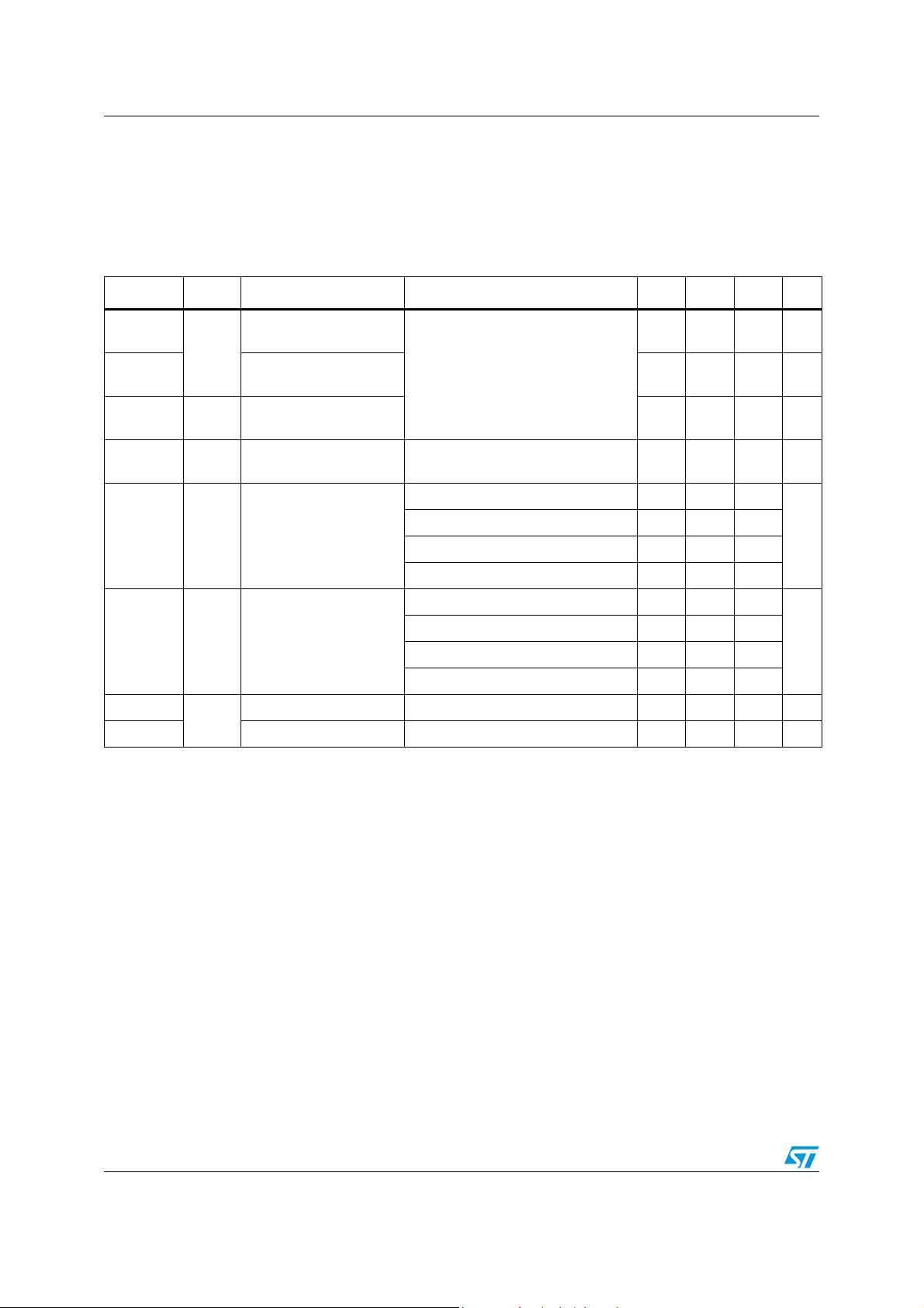
5.1 AC operation
Table 7. AC operation electrical characteristics (VCC = 15 V; TJ =+25 °C)
Symbol Pin Parameter Test condition Min Typ Max Unit
t
on
t
off
t
sd
1 vs 10
3
10, 13
MT
DT 5
High/low side driver turnon propagation delay
vs 13
High/low side driver turnoff propagation delay
2 vs
Shut down to high/low
side propagation delay
Delay matching, HS and
LS turn-on/off
Dead time setting range
(1)
MDT Matching dead time
t
r
t
f
1. See Figure 4 on page 9
2. MDT = | DT
10, 13
LH
Rise time C
Fall time CL = 1 nF 35 70 ns
- DTHL | see Figure 5 on page 13
(2)
= 0 V
V
out
= V
V
boot
CL = 1 nF
cc
50 125 200 ns
50 125 200 ns
Vi = 0 to 3.3 V
See Figure 3
50 125 200 ns
30 ns
R
= 0; CL = 1 nF; CDT = 100 nF 0.1 0.18 0.25
DT
R
= 37 kΩ;CL = 1 nF; CDT=100 nF 0.48 0.6 0.72
DT
= 136 kΩ;CL=1 nF; CDT=100 nF 1.35 1.6 1.85
R
DT
= 260 kΩ;CL=1 nF; CDT=100 nF 2.6 3.0 3.4
R
DT
R
= 0 Ω; CL=1 nF; CDT =100 nF 80
DT
R
= 37 kΩ;CL=1 nF; CDT=100 nF 120
DT
= 136 kΩ;CL=1 nF; CDT=100 nF 250
R
DT
R
= 260 kΩ;CL=1 nF; CDT=100 nF 400
DT
= 1 nF 75 120 ns
L
μs
ns
8/20 Doc ID 14494 Rev 5
Page 9
L6392 Electrical characteristics
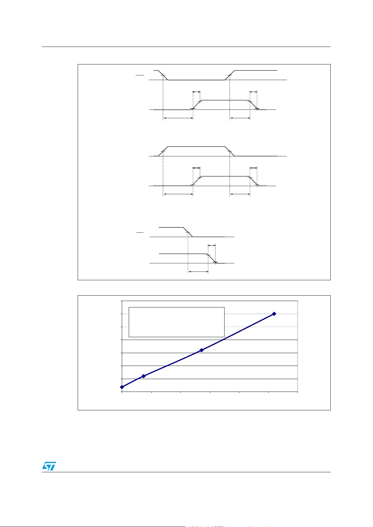
Figure 3. Timing characteristics
LIN
LVG
HIN
HVG
SD
LVG/HVG
50%
50%
50%
tr tf
90%
10%
ton toff
50%
tr tf
90%
10%
ton toff
50%
tf
90%
10%
tsd
90%
10%
90%
10%
Figure 4. Typical dead time vs. DT resistor value
'7XV
$SSUR[LPDWHGIRUPXODIRU
5GWFDOFXODWLRQW\S
5GW>Nȍ@ Â'7>V@
5GWN2KP
Doc ID 14494 Rev 5 9/20
Page 10
Electrical characteristics L6392
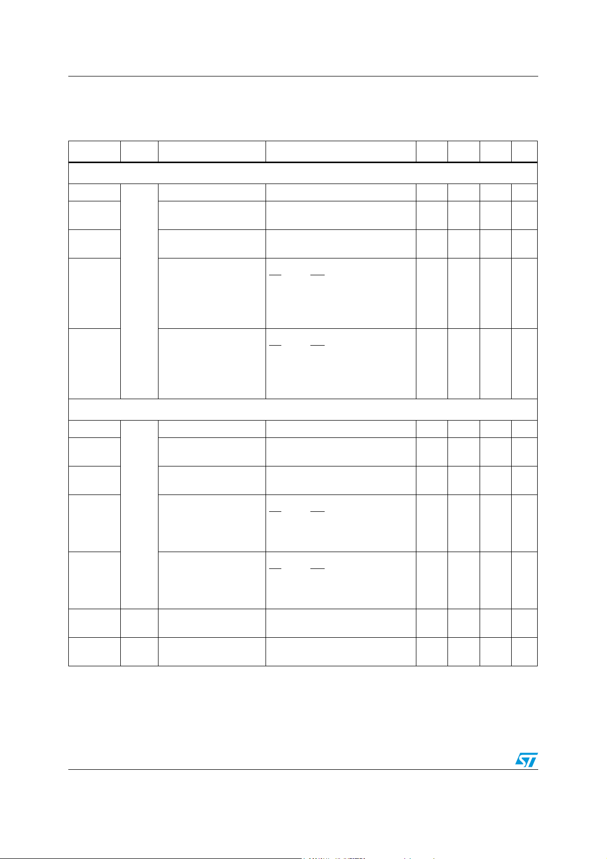
5.2 DC operation
Table 8. DC operation electrical characteristics (VCC = 15 V; TJ = +25 °C)
Symbol Pin Parameter Test condition Min Typ Max Unit
Low supply voltage section
V
cc_hys
V
cc_thON
V
cc_thOFF
I
qccu
I
qcc
4
UV hysteresis 1200 1500 1800 mV
V
cc
Vcc UV turn ON
threshold
Vcc UV turn OFF
threshold
Undervoltage quiescent
supply current
Quiescent current
Bootstrapped supply voltage section
V
BO_hys
V
BO_thON
V
BO_thOFF
I
QBOU
14
UV hysteresis 1200 1500 1800 mV
V
BO
UV turn ON
V
BO
threshold
V
UV turn OFF
BO
threshold
Undervoltage VBO
quiescent current
(1)
VCC = 10 V
= 5 V; LIN = 5 V;
SD
HIN = GND;
= 0 Ω;
R
DT
OP + = GND; OP - = 5 V
V
= 15 V
CC
SD = 5 V; LIN = 5 V;
HIN = GND;
= 0 Ω;
R
DT
OP + = GND; OP - = 5 V
VBO = 9 V
= 5 V; LIN and HIN = 5 V;
SD
= 0 Ω;
R
DT
OP + = GND; OP - = 5 V
11.5 12 12.5 V
10 10.5 11 V
120 150 μA
680 1000 μA
10.6 11.5 12.4 V
9.1 10 10.9 V
70 110 μA
V
= 15 V
BO
= 5 V; LIN and HIN = 5 V;
I
QBO
VBO quiescent current
SD
R
DT
= 0 Ω;
OP + = GND; OP - = 5 V
R
DS(on)
I
LK
High voltage leakage
current
Bootstrap driver on
resistance
(2)
V
= V
out
= V
boot
hvg
LVG ON 120 Ω
10/20 Doc ID 14494 Rev 5
150 210 μA
= 600 V 10 μA
Page 11
L6392 Electrical characteristics
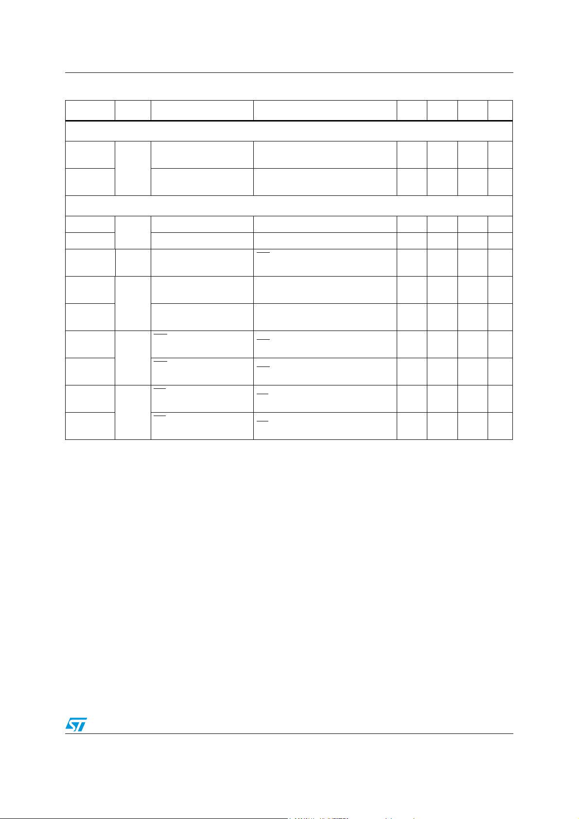
Table 8. DC operation electrical characteristics (VCC = 15 V; TJ = +25 °C) (continued)
Symbol Pin Parameter Test condition Min Typ Max Unit
Driving buffers section
I
so
I
si
Logic inputs
V
il
V
ih
V
il_S
I
HINh
I
HINl
I
LINI
I
LINh
I
SDh
I
SDl
1. VBO = V
2. R
boot
is tested in the following way:
DSon
R
= [(VCC - V
DSon
V
= V
CBOOT
10, 13
1, 2, 3
1, 3
3
1
2
- V
out
CBOOT1
High/low side source
short circuit current
High/low side sink short
circuit current
= V
V
i
Vi = V
< 10 ms) 200 290 mA
ih (tp
< 10 ms) 250 430 mA
il (tp
Low logic level voltage 0.8 V
High logic level voltage 2.25 V
Single input voltage
HIN logic “1” input bias
current
HIN logic “0” input bias
current
LIN
logic “0” input bias
current
LIN logic “1” input bias
current
SD
logic “1” input bias
current
SD logic “0” input bias
current
) - (VCC - V
CBOOT1
, I2 when V
CBOOT
CBOOT2
= V
CBOOT2
LIN and HIN connected together
and floating
HIN = 15 V 110 175 260 μA
HIN = 0 V 1 μA
= 0 V 3 6 20 μA
LIN
= 15 V 1 μA
LIN
SD
= 15 V 10 30 100 μA
= 0 V 1 μA
SD
)] / [I1(VCC,V
CBOOT1
) - I2(VCC,V
)] where I1 is pin 14 current when
CBOOT2
0.8 V
Doc ID 14494 Rev 5 11/20
Page 12
Electrical characteristics L6392
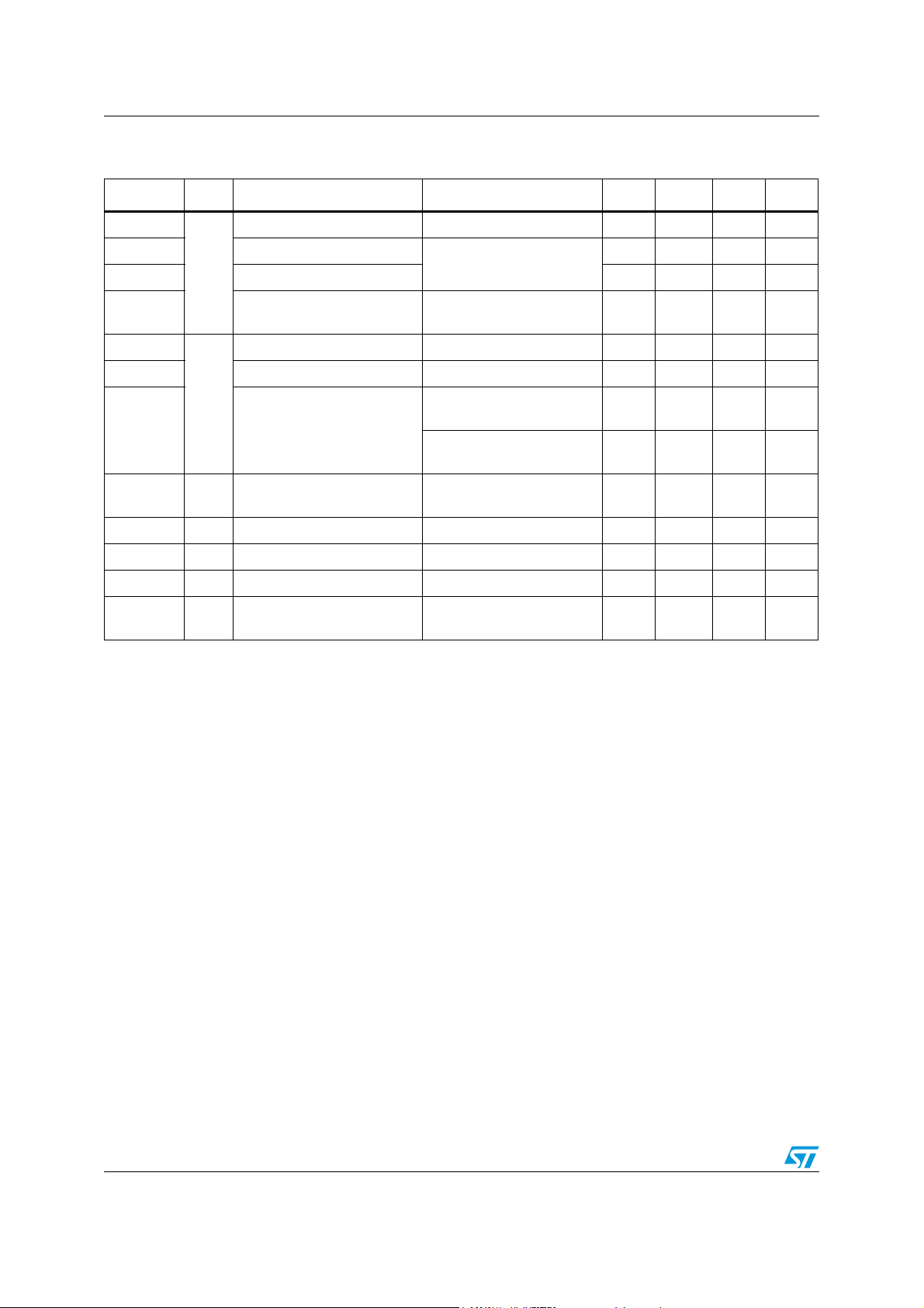
Table 9. OPAMP characteristics (VCC = 15 V, TJ = +25 °C)
Symbol Pin Parameter Test condition Min Typ Max Unit
V
io
I
io
I
ib
V
icm
V
OL
V
OH
Input offset voltage V
Input offset current
8, 9
Input bias current
(1)
Input common mode voltage
range
Low level output voltage R
High level output voltage RL = 10 kΩ to GND 14 14.7 V
6
I
o
Output short circuit current
SR Slew rate
GBWP Gain bandwidth product V
A
vd
Large signal voltage gain RL = 2 kΩ 70 85 dB
SRV Power supply rejection ratio vs V
CMRR
1. The direction of input current is out of the IC.
Common mode rejection
ratio
= 0 V, Vo = 7.5 V 6 mV
ic
440nA
Vic = 0 V, Vo = 7.5 V
100 200 nA
0V
= 10 kΩ to V
L
Source,
V
= + 1 V; Vo = 0 V
id
Sink
= -1 V; Vo = V
V
id
Vi = 1÷4;
= 100 pF; unity gain
C
L
= 7.5 V 8 12 MHz
o
cc
CC
CC
16 30 mA
50 80 mA
2.5 3.8 V/μs
60 75 dB
75 150 mV
-4 V
CC
55 70 dB
12/20 Doc ID 14494 Rev 5
Page 13
L6392 Waveforms definitions
6 Waveforms definitions
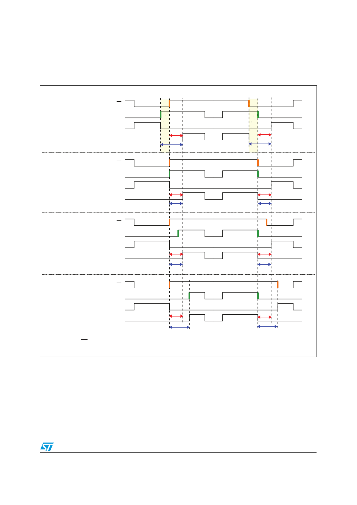
Figure 5. Dead time - timing waveforms
LIN
CONTROL SIGNAL EDGES
OVERLAPPED:
INTERLOCKING + DEAD TIME
CONTROL SIGNALS EDGES
SYNCHRONOUS (*):
DEAD TIME
CONTROL SIGNALS EDGES
NOT OVERLAPPED,
BUT INSIDE THE DEAD TIME:
DEAD TIME
CONTROL SIGNALS EDGES
NOT OVERLAPPED,
OUTSIDE THE DEAD TIME:
DIRECT DRIVING
HIN
LVG
HVG
gate driver outputs OFF
(HALF-BRIDGE TRI-STATE)
LIN
HIN
LVG
HVG
gate driver outputs OFF
(HALF-BRIDGE TRI-STATE)
LIN
HIN
LVG
HVG
gate driver outputs OFF
(HALF-BRIDGE TRI-STATE)
LIN
HIN
LVG
HVG
gate driver outputs OFF
(HALF-BRIDGE TRI-STATE)
INTERLOCKING
DTLH
gate driver outputs OFF
(HALF-BRIDGE TRI-STATE)
DTLH DTHL
gate driver outputs OFF
(HALF-BRIDGE TRI-STATE)
DTLH DTHL
gate driver outputs OFF
(HALF-BRIDGE TRI-STATE)
DTLH
gate driver outputs OFF
(HALF-BRIDGE TRI-STATE)
INTERLOCKING
DTHL
DTHL
(*) HIN and LIN can be connected togheter and driven by just one control signal
Doc ID 14494 Rev 5 13/20
Page 14
Typical application diagram L6392
7 Typical application diagram
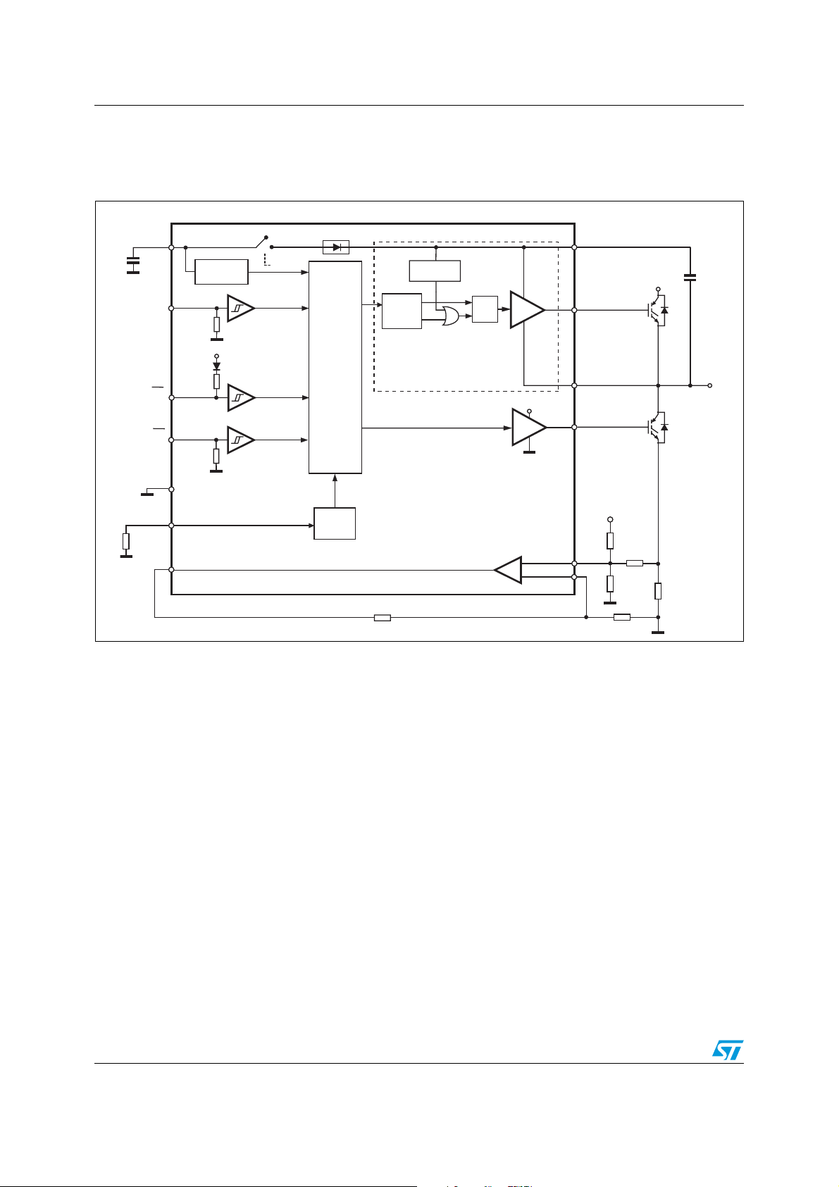
Figure 6. Application diagram
V
CC
OPOUT
GND
HIN
LIN
from LVG
BOOTSTRAP DRIVER
LOGIC
SHOOT
THROUGH
PREVENTION
SD
LATCH
DEAD
TIME
4
UV
DETECTION
3
5V
1
SD
2
7
DT
5
6
FLOATING STRUCTURE
UV
DETECTION
LEVEL
SHIFTER
BOOT
14
HVG
OPAMP
DRIVER
V
CC
DRIVER
+
-
LVG
HVG
13
OUT
12
LVG
10
OP+
8
OP-
9
S
R
H.V.
Cboot
TO LOAD
14/20 Doc ID 14494 Rev 5
Page 15

L6392 Bootstrap driver
8 Bootstrap driver
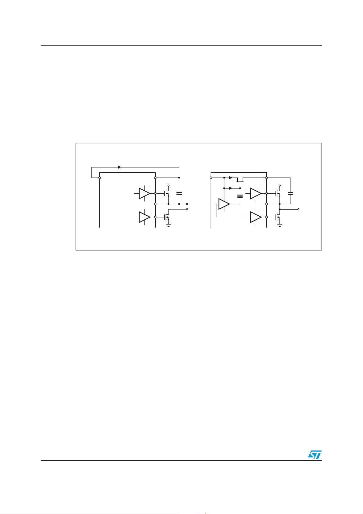
A bootstrap circuitry is needed to supply the high voltage section. This function is normally
accomplished by a high voltage fast recovery diode (Figure 7 a). In the L6392 a patented
integrated structure replaces the external diode. It is realized by a high voltage DMOS,
driven synchronously with the low side driver (LVG), with diode in series, as shown in
Figure 7 b.
An internal charge pump (Figure 7 b) provides the DMOS driving voltage.
8.1 C
To choose the proper C
capacitor. This capacitor C
The ratio between the capacitors C
It has to be:
e.g.: if Q
300 mV.
If HVG has to be supplied for a long time, the C
the leakage and quiescent losses.
e.g.: HVG steady state consumption is lower than 200 μA, so if HVG T
to supply 1 μC to C
The internal bootstrap driver gives a great advantage: the external fast recovery diode can
be avoided (it usually has great leakage current).
BOOT
selection and charging
value the external MOS can be seen as an equivalent
BOOT
is related to the MOS total gate charge:
EXT
C
EXT
and C
EXT
C
BOOT
is 30 nC and V
gate
. This charge on a 1μF capacitor means a voltage drop of 1 V.
EXT
is 10 V, C
gate
EXT
Q
gate
--------------=
V
gate
is proportional to the cyclical voltage loss.
BOOT
>>> C
EXT
is 3 nF. With C
selection has to take into account also
BOOT
= 100 nF the drop would be
BOOT
is 5 ms, C
ON
BOOT
has
This structure can work only if V
LVG is on. The charging time (T
is close to GND (or lower) and in the meanwhile the
OUT
charge
) of the C
is the time in which both conditions are
BOOT
fulfilled and it has to be long enough to charge the capacitor.
The bootstrap driver introduces a voltage drop due to the DMOS R
(typical value:
DSON
120 Ω). At low frequency this drop can be neglected. Anyway increasing the frequency it
must be taken in to account.
The following equation is useful to compute the drop on the bootstrap DMOS:
Q
gate
V
drop
where Q
is the gate charge of the external power MOS, R
gate
bootstrap DMOS, and T
I
==
ch eargRdson
is the charging time of the bootstrap capacitor.
charge
Doc ID 14494 Rev 5 15/20
→
V
drop
------------------
T
ch earg
dson
R
dson
is the on resistance of the
Page 16
Bootstrap driver L6392
D
For example: using a power MOS with a total gate charge of 30 nC the drop on the
bootstrap DMOS is about 1 V, if the T
V
drop
V
has to be taken into account when the voltage drop on C
drop
is 5 μs. In fact:
charge
30nC
-------------- -
5μs
120Ω 0.7V∼⋅=
is calculated: if this drop
BOOT
is too high, or the circuit topology doesn’t allow a sufficient charging time, an external diode
can be used.
Figure 7. Bootstrap driver
D
BOOT
S
HVG
LVG
BOOTV
H.V.
C
BOOT
V
OUT
TO LOAD
V
S
HVG
LVG
ab
BOOT
V
OUT
H.V.
C
BOOT
TO LOA
D99IN1067
16/20 Doc ID 14494 Rev 5
Page 17
L6392 Package mechanical data
9 Package mechanical data
In order to meet environmental requirements, ST offers these devices in different grades of
ECOPACK
specifications, grade definitions and product status are available at: www.st.com.
ECOPACK
®
packages, depending on their level of environmental compliance. ECOPACK®
®
is an ST trademark.
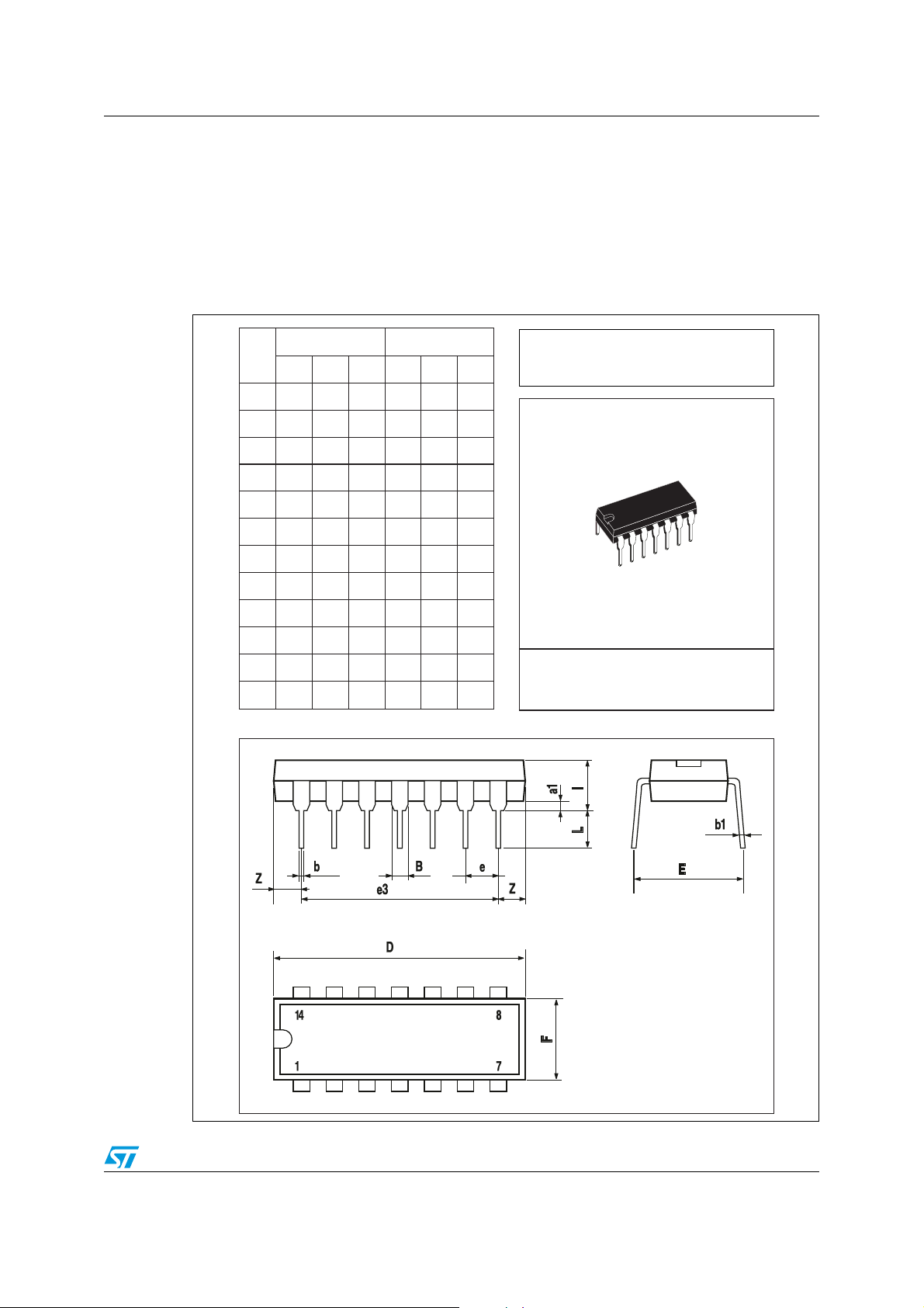
Figure 8. DIP-14 mechanical data and package dimensions
DIM.
a1 0.51 0.020
B 1.39 1.65 0.055 0.065
b 0.5 0.020
b1 0.25 0.010
D 20 0.787
E 8.5 0.335
e 2.54 0.100
e3 15.24 0.600
F 7.1 0.280
I 5.1 0.201
mm inch
MIN. TYP. MAX. MIN. TYP. MAX.
OUTLINE AND
MECHANICAL DATA
L 3.3 0.130
Z 1.27 2.54 0.050 0.100
DIP14
Doc ID 14494 Rev 5 17/20
Page 18
Package mechanical data L6392
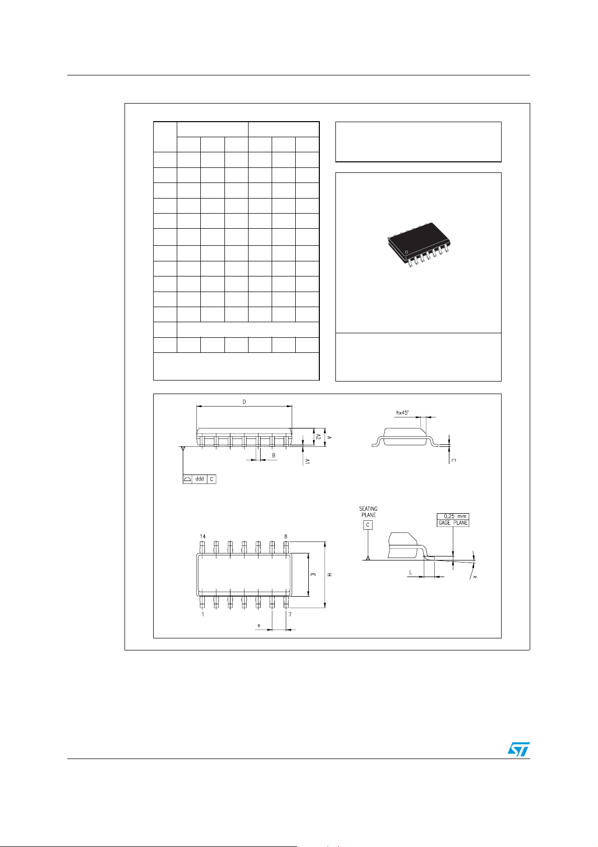
Figure 9. SO-14 mechanical data and package dimensions
DIM.
A 1.35 1.75 0.053 0.069
A1 0.10 0.30 0.004 0.012
A2 1.10 1.65 0.043 0.065
B 0.33 0.51 0.013 0.020
C 0.19 0.25 0.007 0.01
(1)
D
E 3.80 4.0 0.150 0.157
e 1.27 0.050
H 5.8 6.20 0.228 0.2 44
h 0.25 0.50 0.01 0. 02
L 0.40 1.27 0.016 0.050
k 0˚ (min.), 8˚ (max.)
ddd 0.10 0.004
(1) “D” dimensio n does not include mold flash, prot usions or gate
burrs. Mol d flash, protusions o r gate burrs shall not exceed
0.15mm per sid e.
mm inch
MIN. TYP. MAX. MIN. TYP. MAX.
8.55 8.75 0.337 0.344
OUTLINE AND
MECHANICAL DATA
SO14
18/20 Doc ID 14494 Rev 5
0016019 D
Page 19
L6392 Revision history
10 Revision history
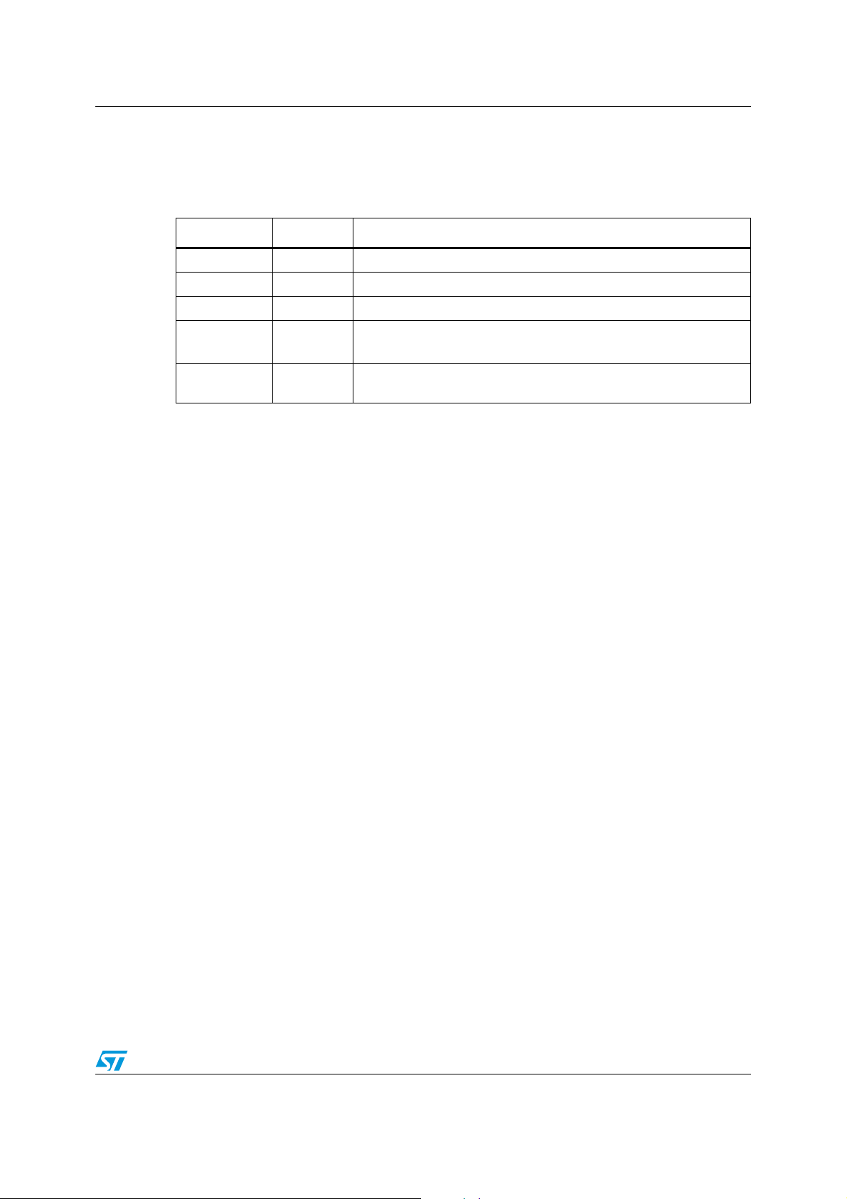
Table 10. Document revision history
Date Revision Changes
29-Feb-2008 1 Initial release
18-Mar-2008 2 Cover page updated
17-Sep-2008 3 Updated Table 4 on page 6, Table 4 on page 6, Table 9 on page 12
17-Feb-2009 4
11-Aug-2010 5
Updated Table 7 on page 8, Table 8 on page 10, Table 9 on page 12
Added Table 4 on page 9
Updated cover page, Table 1 on page 1, Table 7 on page 8, Ta ble 9
on page 12
Doc ID 14494 Rev 5 19/20
Page 20

L6392
Please Read Carefully:
Information in this document is provided solely in connection with ST products. STMicroelectronics NV and its subsidiaries (“ST”) reserve the
right to make changes, corrections, modifications or improvements, to this document, and the products and services described herein at any
time, without notice.
All ST products are sold pursuant to ST’s terms and conditions of sale.
Purchasers are solely responsible for the choice, selection and use of the ST products and services described herein, and ST assumes no
liability whatsoever relating to the choice, selection or use of the ST products and services described herein.
No license, express or implied, by estoppel or otherwise, to any intellectual property rights is granted under this document. If any part of this
document refers to any third party products or services it shall not be deemed a license grant by ST for the use of such third party products
or services, or any intellectual property contained therein or considered as a warranty covering the use in any manner whatsoever of such
third party products or services or any intellectual property contained therein.
UNLESS OTHERWISE SET FORTH IN ST’S TERMS AND CONDITIONS OF SALE ST DISCLAIMS ANY EXPRESS OR IMPLIED
WARRANTY WITH RESPECT TO THE USE AND/OR SALE OF ST PRODUCTS INCLUDING WITHOUT LIMITATION IMPLIED
WARRANTIES OF MERCHANTABILITY, FITNESS FOR A PARTICULAR PURPOSE (AND THEIR EQUIVALENTS UNDER THE LAWS
OF ANY JURISDICTION), OR INFRINGEMENT OF ANY PATENT, COPYRIGHT OR OTHER INTELLECTUAL PROPERTY RIGHT.
UNLESS EXPRESSLY APPROVED IN WRITING BY AN AUTHORIZED ST REPRESENTATIVE, ST PRODUCTS ARE NOT
RECOMMENDED, AUTHORIZED OR WARRANTED FOR USE IN MILITARY, AIR CRAFT, SPACE, LIFE SAVING, OR LIFE SUSTAINING
APPLICATIONS, NOR IN PRODUCTS OR SYSTEMS WHERE FAILURE OR MALFUNCTION MAY RESULT IN PERSONAL INJURY,
DEATH, OR SEVERE PROPERTY OR ENVIRONMENTAL DAMAGE. ST PRODUCTS WHICH ARE NOT SPECIFIED AS "AUTOMOTIVE
GRADE" MAY ONLY BE USED IN AUTOMOTIVE APPLICATIONS AT USER’S OWN RISK.
Resale of ST products with provisions different from the statements and/or technical features set forth in this document shall immediately void
any warranty granted by ST for the ST product or service described herein and shall not create or extend in any manner whatsoever, any
liability of ST.
ST and the ST logo are trademarks or registered trademarks of ST in various countries.
Information in this document supersedes and replaces all information previously supplied.
The ST logo is a registered trademark of STMicroelectronics. All other names are the property of their respective owners.
© 2010 STMicroelectronics - All rights reserved
STMicroelectronics group of companies
Australia - Belgium - Brazil - Canada - China - Czech Republic - Finland - France - Germany - Hong Kong - India - Israel - Italy - Japan -
Malaysia - Malta - Morocco - Philippines - Singapore - Spain - Sweden - Switzerland - United Kingdom - United States of America
www.st.com
20/20 Doc ID 14494 Rev 5
 Loading...