

Page 1
L6229
Fi
DMOS DRIVER FOR
THREE-PHASE BRUSHLESS DC MOTOR
1FEATURES
■ OPERATING SUPPLY VOLTAGE FROM 8 TO
52V
■ 2.8A OUTPUT PEAK CURRENT (1.4A DC)
■ R
■ OPERATING FREQUENCY UP TO 100KHz
■ NON DISSIPATIVE OVERCURRENT
0.73Ω TYP. VALUE @ Tj = 25 °C
DS(ON)
DETECTION AND PROTECTION
■ DIAGNOSTIC OUTPUT
■ CONSTANT t
PWM CURRENT
OFF
CONTROLLER
■ SLOW DECAY SYNCHR. RECTIFICATION
■ 60° & 120° HALL EFFECT DECODING LOGIC
■ BRAKE FUNCTION
■ TACHO OUTPUT FOR SPEED LOOP
■ CROSS CONDUCTION PROTECTION
■ THERMAL SHUTDOWN
■ UNDERVOLTAGE LOCKOUT
■ INTEGRATED FAST FREEWEELING DIODES
2 DESCRIPTION
The L6229 is a DMOS Fully Integrated Three-Phase
Motor Driver with Overcurrent Protection.
Realized in MultiPower-BCD technology, the device
combines isolated DMOS Power Transistors with
CMOS and bipolar circuits on the same chip.
The device includes all the circuitry needed to drive a
three-phase BLDC motor including: a three-phase
DMOS Bridge, a constant off time PWM Current Controller and the decoding logic for single ended hall
sensors that generates the required sequence for the
power stage.
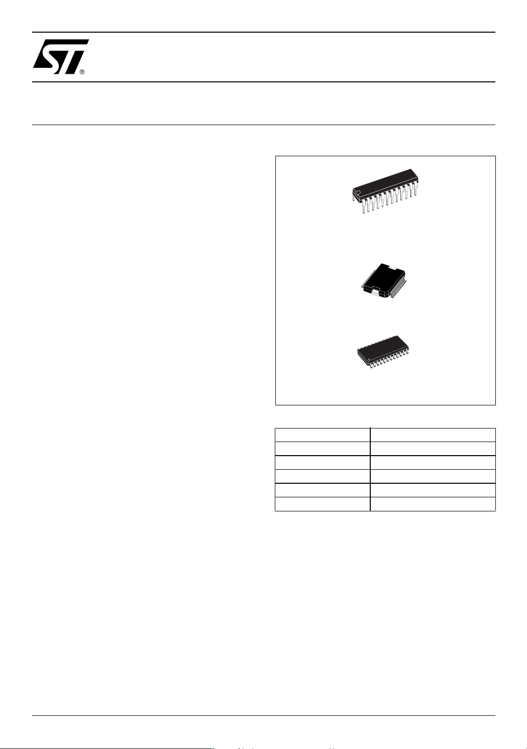
Available in PowerDIP24 (20+2+2), PowerSO36 and
SO24 (20+2+2) packages, the L6229 features a non-
gure 1. Package
PowerDIP24
(20+2+2)
PowerSO36
SO24
(20+2+2)
Table 1. Order Codes
Part Number Package
L6229N PowerDIP24
L6229PD PowerSO36
L6229PDTR PowerSO36 in Tape & Reel
L6229D SO24
L6229DTR SO24 in Tape & Reel
dissipative overcurrent protection on the high side
Power MOSFETs and thermal shutdown.
October 2004
Rev. 3
1/25
Page 2
L6229
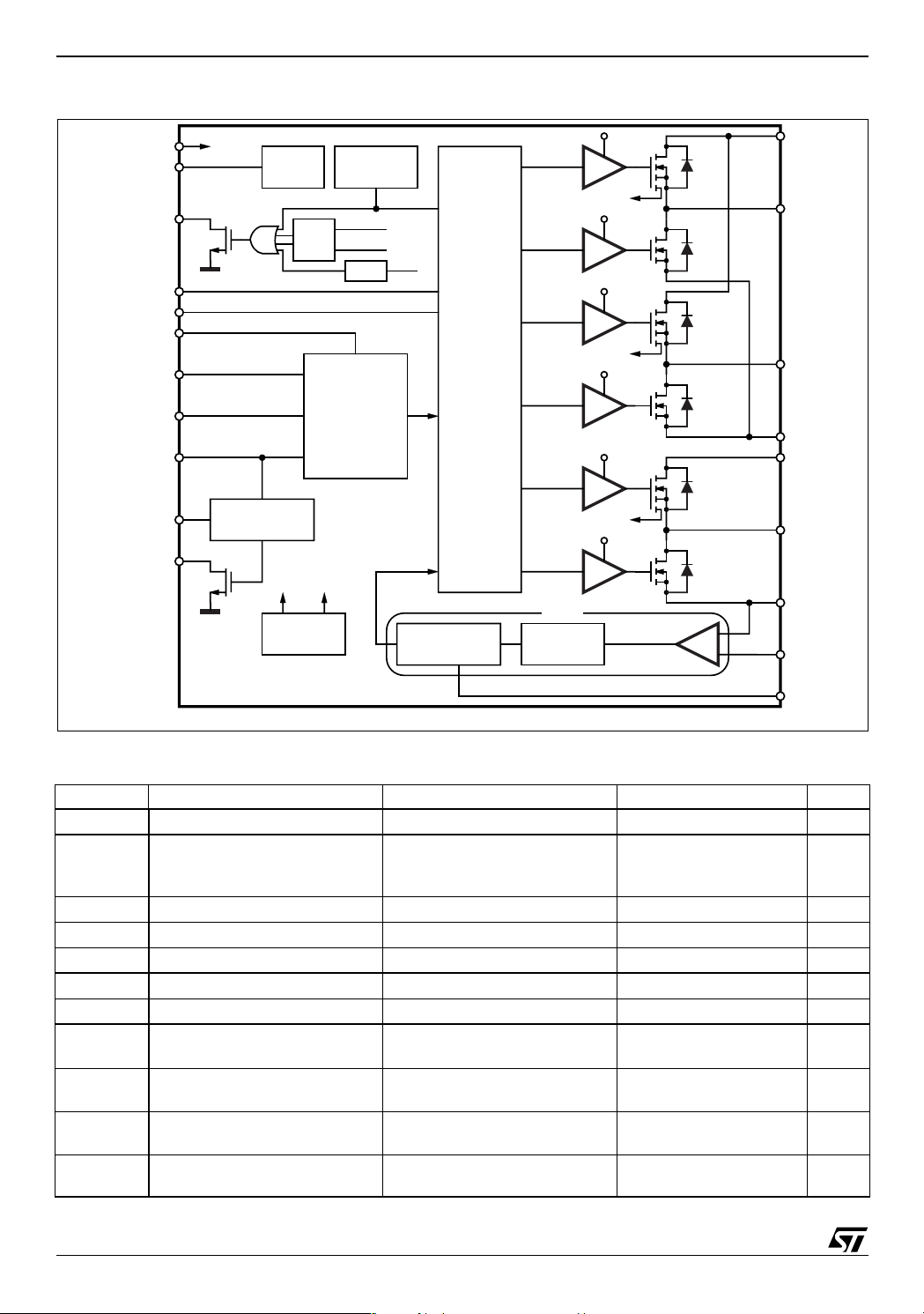
Figure 2. Block Diagram
VBOOT V
VCP
DIAG
EN
BRAKE
FWD/REV
H
3
H
2
H
1
RCPULSE
TACHO
BOOT
CHARGE
PUMP
TACHO
MONOSTABLE
10V
VOLTAGE
REGULATOR
THERMAL
PROTECTION
OCD1
OCD
OCD2
HALL-EFFECT
SENSORS
DECODING
LOGIC
5V
OCD
OCD3
ONE SHOT
MONOSTABLE
GATE
LOGIC
PWM
MASKING
TIME
V
BOOT
OCD1
10V
V
BOOT
OCD2
10V
V
BOOT
OCD3
10V
COMPARATOR
SENSE
VS
A
OUT
1
OUT
2
SENSE
A
VS
B
OUT
3
SENSE
B
+
-
VREF
RCOFF
D99IN1095B
Table 2. Absolute Maximum Ratings
Symbol Parameter Test conditions Value Unit
V
V
V
RCPULSE
V
I
T
2/25
V
V
OD
V
BOOT
, V
IN
V
REF
RCOFF
SENSE
S(peak)
I
S
, T
stg
Supply Voltage VSA = VSB = V
S
Differential Voltage between:
VS
, OUT1, OUT2, SENSEA
A
and VS
, OUT3, SENSE
B
B
VSA = VSB = VS = 60V;
V
SENSEA
Bootstrap Peak Voltage VSA = VSB = V
Logic Inputs Voltage Range -0.3 to 7 V
EN
= V
S
SENSEB
S
= GND
60 V
60 V
VS + 10 V
Voltage Range at pin VREF -0.3 to 7 V
Voltage Range at pin RCOFF -0.3 to 7 V
Voltage Range at pin RCPULSE -0.3 to 7 V
Voltage Range at pins SENSEA
and SENSE
B
Pulsed Supply Current (for each
VS
and VSB pin)
A
DC Supply Current (for each
VS
and VSB pin)
A
Storage and Operating
OP
= VSB = VS; T
V
SA
= VSB = V
V
SA
S
< 1ms 3.55 A
PULSE
-1 to 4 V
1.4 A
-40 to 150 °C
Temperature Range
Page 3

Table 3. Recommended Operating Condition
Symbol Parameter Test Conditions MIN MAX Unit
L6229
V
V
V
SENSE
I
OUT
f
V
OD
REF
T
SW
Supply Voltage VSA = VSB = V
S
Differential Voltage between:
VS
, OUT1, OUT2, SENSEA and
A
, OUT3, SENSE
VS
B
VSA = VSB = VS;
V
SENSEA
B
= V
S
SENSEB
Voltage Range at pin VREF -0.1 5 V
Voltage Range at pins SENSEA
and SENSE
B
DC Output Current VSA = VSB = V
Operating Junction Temperature -25 125 °C
J
(pulsed tW < trr)
(DC)
S
Switching Frequency 100 KHz
Table 4. Thermal Data
Symbol Description PDIP24 SO24
R
th(j-pins)
R
th(j-case)
R
th(j-amb)1
Maximum Thermal Resistance Junction-Pins 19 15 °C/W
Maximum Thermal Resistance Junction-Case 2 °C/W
MaximumThermal Resistance Junction-Ambient
(1)
44 55 - °C/W
12 52 V
52 V
-6
-1
6
1
1.4 A
PowerSO36
Unit
V
V
(3)
(2)
(4)
--36°C/W
--16°C/W
59 78 63 °C/W
R
th(j-amb)1
R
th(j-amb)1
R
th(j-amb)2
(1) Mounted on a multi-layer FR4 PCB with a dissipating copper surface on the bottom side of 6 cm2 (with a thickness of 35 µm).
(2) Mounted on a multi-layer FR4 PCB with a dissipating copper surface on the top side of 6 cm2 (with a thickness of 35 µm).
(3) Mounted on a multi-layer FR4 PCB with a dissipating copper surface on the top side of 6 cm2 (with a thickness of 35 µm),
(4) Mounted on a multi-layer FR4 PCB without any heat-sinking surface on the board.
Maximum Thermal Resistance Junction-Ambient
MaximumThermal Resistance Junction-Ambient
Maximum Thermal Resistance Junction-Ambient
16 via holes and a ground layer.
3/25
Page 4
L6229
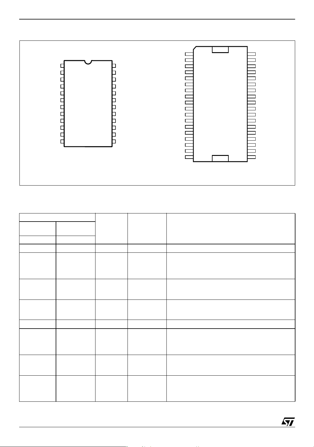
Figure 3. Pin Connections (Top view)
DIAG
SENSE
RCOFF
OUT
GND
GND
TACHO
RCPULSE
SENSE
FWD/REV
EN
1
H
1
2
3
A
4
5
1
6
7
8
9
10
B
11
12
PowerDIP24/SO24
D01IN1194A
GND
N.C.
24
H
3
23
H
2
22
VCP
21
OUT
2
VS
20
18
17
16
15
14
13
A
GND19
GND
VS
B
OUT
3
VBOOT
BRAKE
VREF
N.C.
VS
OUT
N.C.
VCP
DIAG
SENSE
RCOFF
N.C.
OUT
N.C.
N.C.
GND
1
2
3
4
A
5
2
7
H
8
2
H
3
H
10
1
11
12
A
13
14
15
1
16
17
18
D01IN1195A
PowerSO36
36
35
34
33
32
31
30
29
28
27
26
25
24
23
22
21
20
19
(5)
(5) The slug is internally connected to pins 1, 18, 19 and 36 (GND pins).
Table 5. Pin Description
PACKAGE
SO24/
PowerDIP24
PowerSO36
PIN # PIN #
110H
2 11 DIAG Open Drain
3 12 SENSE
4 13 RCOFF RC Pin RC Network Pin. A parallel RC network connected
515OUT
6, 7,
18, 19
1, 18,
19, 36
8 22 TACHO Open Drain
9 24 RCPULSE RC Pin RC Network Pin. A parallel RC network connected
Name Type Function
1
Sensor Input Single Ended Hall Effect Sensor Input 1.
Overcurrent Detection and Thermal Protection pin. An
Output
internal open drain transistor pulls to GND when an
overcurrent on one of the High Side MOSFETs is
detected or during Thermal Protection.
Power Supply Half Bridge 1 and Half Bridge 2 Source Pin. This pin
A
must be connected together with pin SENSE
Power Ground through a sensing power resistor.
between this pin and ground sets the Current
Controller OFF-Time.
Power Output Output 1
1
GND GND Ground terminals. On PowerDIP24 and SO24
packages, these pins are also used for heat
dissipation toward the PCB. On PowerSO36 package
the slug is connected on these pins.
Frequency-to-Voltage open drain output. Every pulse
Output
from pin H
is shaped as a fixed and adjustable length
1
pulse.
between this pin and ground sets the duration of the
Monostable Pulse used for the Frequency-to-Voltage
converter.
GND
N.C.
N.C.
VS
B
OUT
3
N.C.6
VBOOT
BRAKE
VREF9
EN
FWD/REV
SENSE
B
RCPULSE
N.C.
TACHO
N.C.
N.C.
GND
B
to
4/25
Page 5

Table 5. Pin Description (continued)
PACKAGE
SO24/
PowerDIP24
PowerSO36
PIN # PIN #
10 25 SENSE
11 26 FWD/REV Logic Input Selects the direction of the rotation. HIGH logic level
12 27 EN Logic Input Chip Enable. LOW logic level switches OFF all Power
13 28 VREF Logic Input Current Controller Reference Voltage.
14 29 BRAKE Logic Input Brake Input pin. LOW logic level switches ON all High
15 30 VBOOT Supply Voltage Bootstrap Voltage needed for driving the upper Power
16 32 OUT
17 33 VS
20 4 VS
21 5 OUT
22 7 VCP Output Charge Pump Oscillator Output.
23 8 H
24 9 H
Name Type Function
Power Supply Half Bridge 3 Source Pin. This pin must be connected
B
together with pin SENSE
to Power Ground through a
A
sensing power resistor. At this pin also the Inverting
Input of the Sense Comparator is connected.
sets Forward Operation, whereas LOW logic level sets
Reverse Operation.
If not used, it has to be connected to GND or +5V..
MOSFETs.
If not used, it has to be connected to +5V.
Do not leave this pin open or connect to GND.
Side Power MOSFETs, implementing the Brake
Function.
If not used, it has to be connected to +5V.
MOSFETs.
Power Output Output 3.
3
Power Supply Half Bridge 3 Power Supply Voltage. It must be
B
connected to the supply voltage together with pin VS
Power Supply Half Bridge 1 and Half Bridge 2 Power Supply Voltage.
A
It must be connected to the supply voltage together
with pin VS
Power Output Output 2.
2
2
3
Sensor Input Single Ended Hall Effect Sensor Input 2.
Sensor Input Single Ended Hall Effect Sensor Input 3.
.
B
L6229
A
.
Table 6. Electrical Characteristics
(V
= 48V , T
S
Symbol Parameter Test Conditions Min Typ Max Unit
V
Sth(ON)
V
Sth(OFF)
T
J(OFF)
Turn ON threshold 5.8 6.3 6.8 V
Turn OFF threshold 5 5.5 6 V
Quiescent Supply Current All Bridges OFF;
I
S
Thermal Shutdown Temperature 165 °C
Output DMOS Transistors
R
DS(ON)
High-Side + Low-Side Switch ON
Resistance
I
Leakage Current EN = Low; OUT = V
DSS
= 25 °C , unless otherwise specified)
amb
Tj = -25 to 125°C
Tj = 25 °C 1.47 1.69 Ω
T
=125 °C
j
EN = Low; OUT = GND -0.3 mA
(7)
(6)
CC
510mA
2.35 2.70 Ω
2mA
5/25
Page 6
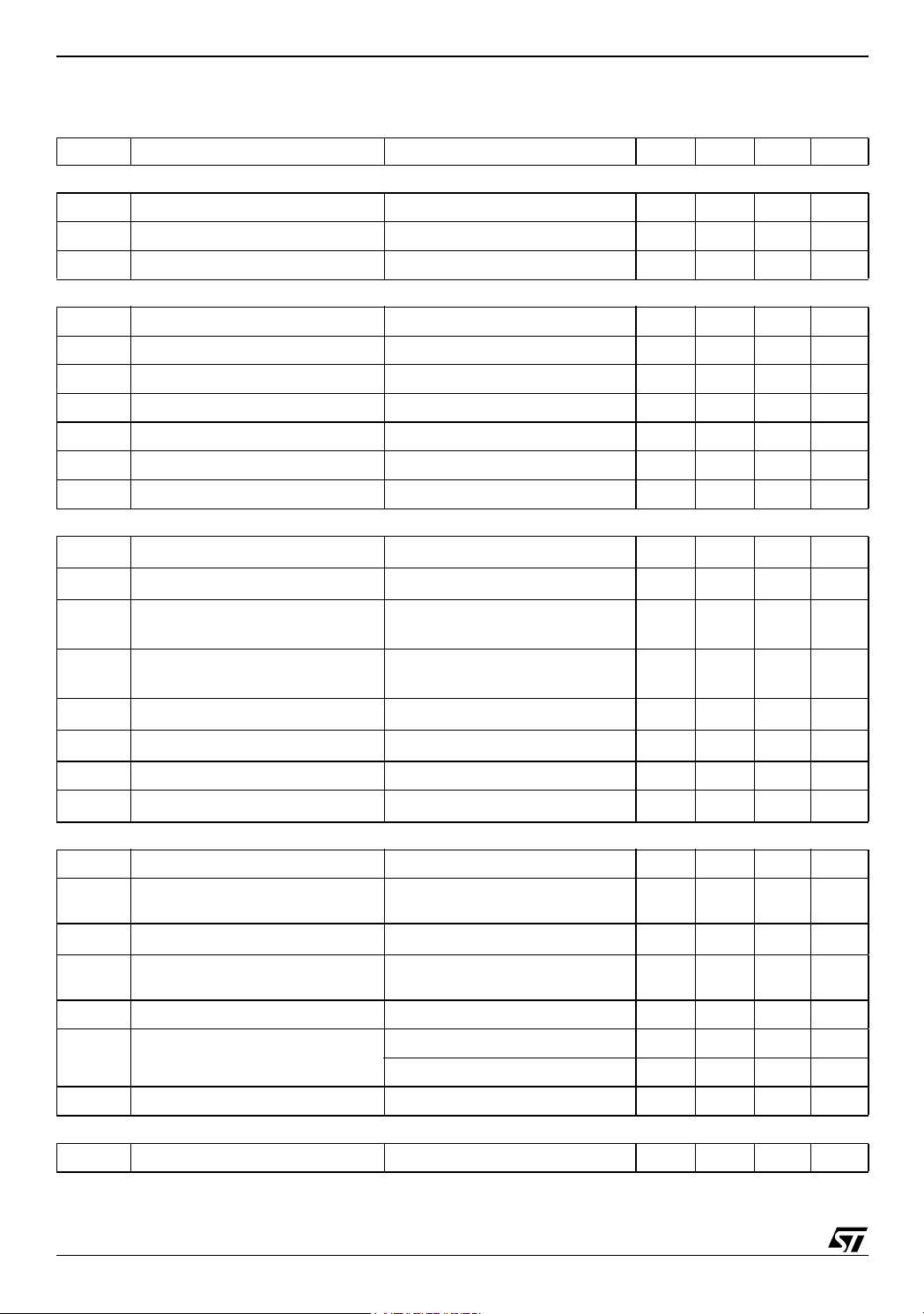
L6229
Table 6. Electrical Characteristics (continued)
(V
= 48V , T
S
Symbol Parameter Test Conditions Min Typ Max Unit
Source Drain Diodes
V
Forward ON Voltage ISD = 1.4A, EN = LOW 1.15 1.3 V
SD
t
Reverse Recovery Time If = 1.4A 300 ns
rr
t
Forward Recovery Time 200 ns
fr
Logic Input (H1, H2, H3, EN, FWD/REV, BRAKE)
Low level logic input voltage -0.3 0.8 V
V
IL
V
High level logic input voltage 2 7 V
IH
I
Low level logic input current GND Logic Input Voltage -10 µA
IL
High level logic input current 7V Logic Input Voltage 10 µA
I
IH
V
th(ON)
V
th(OFF)
V
thHYS
Turn-ON Input Threshold 1.8 2.0 V
Turn-OFF Input Threshold 0.8 1.3 V
Input Thresholds Hysteresys 0.25 0.5 V
Switching Characteristics
t
D(on)EN
t
D(off)EN
t
D(on)IN
Enable to out turn-ON delay time
Enable to out turn-OFF delay time
Other Logic Inputs to Output TurnON delay Time
t
D(off)IN
Other Logic Inputs to out Turn-OFF
delay Time
t
RISE
t
FAL L
Output Rise Time
Output Fall Time
Dead Time 0.5 1 µs
t
DT
Charge Pump Frequency
f
CP
PWM Comparator and Monostable
I
RCOFF
V
OFFSET
Source current at pin RC
Offset Voltage on Sense
Comparator
t
prop
Turn OFF Propagation delay
t
blank
Internal Blanking Time on Sense
Comparator
t
ON(min)
t
I
BIAS
Minimum on Time
PWM RecirculationTime R
OFF
Input Bias Current at pin VREF 10 µA
Tacho Monostable
I
RCPULSE
Source Current at pin RCPULSE V
= 25 °C , unless otherwise specified)
amb
(7)
I
LOAD
(7
)
I
LOAD
I
LOAD
I
LOAD
(7)
(7)
I
LOAD
I
LOAD
Tj = -25 to 125°C
V
OFF
(8)
RCOFF
V
ref
V
ref
OFF
R
OFF
RCPULSE
= 1.4 A, Resistive Load 500 650 800 ns
= 1.4 A, Resistive Load 500 1000 ns
= 1.4 A, Resistive Load 1.6 µs
= 1.4 A, Resistive Load 800 ns
= 1.4 A, Resistive Load 40 250 ns
= 1.4 A, Resistive Load 40 250 ns
(6)
0.6 1 MHz
= 2.5 V 3.5 5.5 mA
= 0.5 V ±5 mV
= 0.5 V 500 ns
1µs
2.5 3 µs
= 20kΩ ; C
= 100kΩ ; C
OFF
OFF
=1nF
=1nF
13
61
= 2.5V 3.5 5.5 mA
µs
µs
6/25
Page 7
L6229
Table 6. Electrical Characteristics (continued)
(V
= 48V , T
S
Symbol Parameter Test Conditions Min Typ Max Unit
t
PULSE
R
TACHO
Monostable of Time R
Open Drain ON Resistance 40 60 Ω
Over Current Detection & Protection
I
SOVER
Supply Overcurrent Protection
Threshold
R
OPDR
t
OCD(ON)
t
OCD(OFF)
(6) Tested at 25°C in a restricted range and guaranteed by characterization.
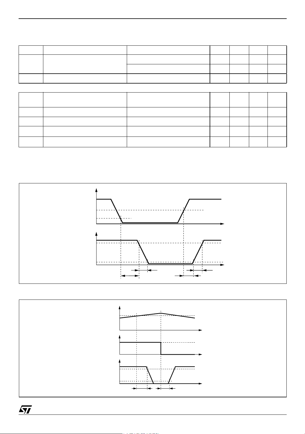
(7) See Fig. 4.
(8) Measured applying a voltage of 1V to pin SENSE and a voltage drop from 2V to 0V to pin VREF.
(9) See Fig. 5.
Open Drain ON Resistance I
OCD high level leakage current V
I
OH
OCD Turn-ON Delay Time
OCD Turn-OFF Delay Time
Figure 4. Switching Characteristic Definition
= 25 °C , unless otherwise specified)
amb
PUL
R
PUL
= -25 to 125°C
T
J
DIAG
DIAG
(9)
(9)
I
DIAG
I
DIAG
= 20kΩ ; C
= 100kΩ ; C
PUL
PUL
(6)
=1nF
=1nF
12
60
2 2.8 3.55 A
= 4mA 40 60 Ω
= 5V 1 µA
= 4mA; C
= 4mA; C
< 100pF 200 ns
DIAG
< 100pF 100 ns
DIAG
µs
µs
EN
V
th(ON)
V
th(OFF)
I
OUT
90%
10%
D01IN1316
t
D(OFF)EN
Figure 5. Overcurrent Detection Timing Definition
I
OUT
I
SOVER
ON
BRIDGE
OFF
V
DIAG
90%
t
FALL
t
D(ON)EN
t
RISE
t
t
10%
t
OCD(ON)
t
OCD(OFF)
D02IN1387
7/25
Page 8
L6229
3 CIRCUIT DESCRIPTION
3.1 POWER STAGES and CHARGE PUMP
The L6229 integrates a Three-Phase Bridge, which consists of 6 Power MOSFETs connected as shown on the
Block Diagram. Each Power MOS has an R
diode. Switching patterns are generated by the PWM Current Controller and the Hall Effect Sensor Decoding
Logic (see relative paragraphs). Cross conduction protection is implemented by using a dead time (t
typical value) set by internal timing circuit between the turn off and turn on of two Power MOSFETs in one leg
of a bridge.
Pins VS
and VSB MUST be connected together to the supply voltage (VS).
A
Using N-Channel Power MOS for the upper transistors in the bridge requires a gate drive voltage above the
power supply voltage. The Bootstrapped Supply (V
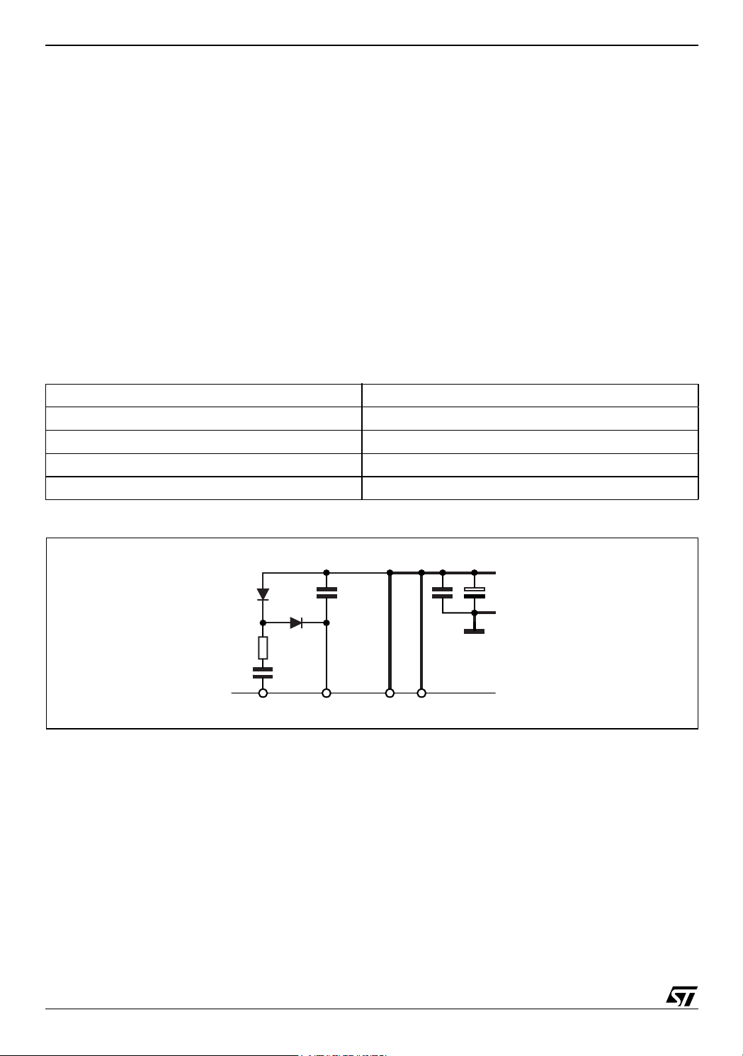
ternal components to realize a charge pump circuit as shown in Figure 6. The oscillator output (pin VCP) is a
square wave at 600KHz (typically) with 10V amplitude. Recommended values/part numbers for the charge
pump circuit are shown in Table 7.
Table 7. Charge Pump External Component Values.
C
BOOT
C
P
R
P
D
1
D
2
= 0.73Ω (typical value @25°C) with intrinsic fast freewheeling
DS(ON)
) is obtained through an internal oscillator and few ex-
BOOT
220nF
10nF
100Ω
1N4148
1N4148
DT
= 1µs
Figure 6. Charge Pump Circuit
V
S
D1
D2
R
P
C
P
VCP VBOOT VS
C
BOOT
VS
B
D01IN1328
A
3.2 LOGIC INPUTS
Pins FWD/REV, BRAKE, EN, H1, H2 and H3 are TTL/CMOS and µC compatible logic inputs. The internal structure is shown in Figure 4. Typical value for turn-ON and turn-OFF thresholds are respectively V
th(OFF)
= 1.3V.
V
th(ON)
= 1.8V and
Pin EN (enable) may be used to implement Overcurrent and Thermal protection by connecting it to the open collector
DIAG output If the protection and an external disable function are both desired, the appropriate connection must be
implemented. When the external signal is from an open collector output, the circuit in Figure 8 can be used . For external circuits that are push pull outputs the circuit in Figure 9 could be used. The resistor R
Ω
the range from 2.2K
to 180KΩ. Recommended values for REN and CEN are respectively 100KΩ and 5.6nF. More
should be chosen in
EN
information for selecting the values can be found in the Overcurrent Protection section.
8/25
Page 9
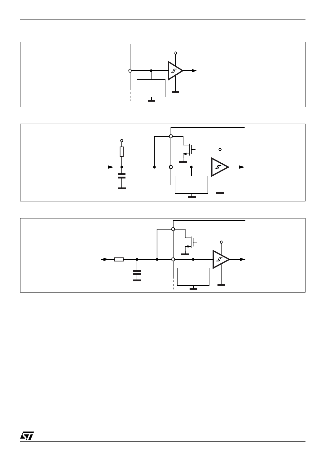
Figure 7. Logic Input Internal Structure
8
Figure 8. Pin EN Open Collector Driving
L6229
5V
ESD
PROTECTION
D01IN1329
OPEN
COLLECTOR
OUTPUT
Figure 9. Pin EN Push-Pull Driving
PUSH-PULL
OUTPUT
R
3.3 PWM CURRENT CONTROL
EN
5V
DIAG
R
EN
C
EN
C
EN
EN
ESD
PROTECTION
DIAG
EN
ESD
PROTECTION
5V
D02IN137
5V
D02IN1379
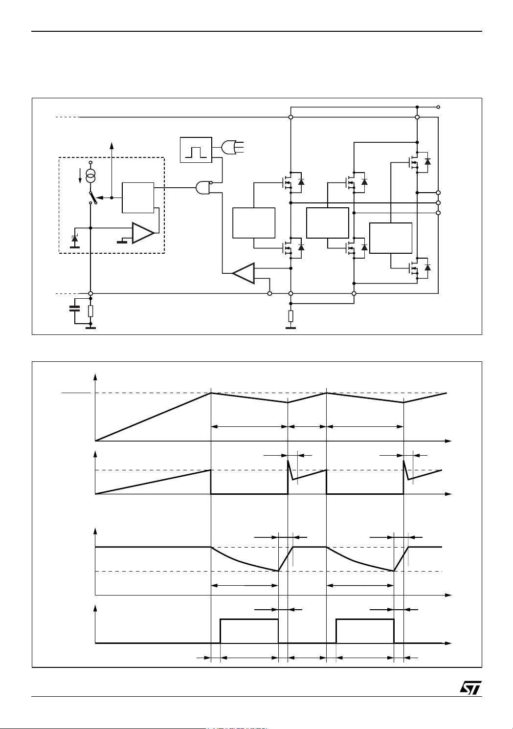
The L6229 includes a constant off time PWM Current Controller. The current control circuit senses the bridge
current by sensing the voltage drop across an external sense resistor connected between the source of the
three lower power MOS transistors and ground, as shown in Figure 10. As the current in the motor increases
the voltage across the sense resistor increases proportionally. When the voltage drop across the sense resistor
becomes greater than the voltage at the reference input pin VREF the sense comparator triggers the
monostable switching the bridge off. The power MOS remain off for the time set by the monostable and the motor current recirculates around the upper half of the bridge in Slow Decay Mode as described in the next section.
When the monostable times out, the bridge will again turn on. Since the internal dead time, used to prevent
cross conduction in the bridge, delays the turn on of the power MOS, the effective Off Time t
is the sum of
OFF
the monostable time plus the dead time.
Figure 11 shows the typical operating waveforms of the output current, the voltage drop across the sensing resistor, the pin RC voltage and the status of the bridge. More details regarding the Synchronous Rectification and
the output stage configuration are included in the next section.
Immediately after the Power MOS turn on, a high peak current flows through the sense resistor due to the re-
9/25
Page 10
L6229
verse recovery of the freewheeling diodes. The L6229 provides a 1µs Blanking Time t
comparator output so that the current spike cannot prematurely retrigger the monostable.
Figure 10. PWM Current Controller Simplified Schematic
VS
B
S
BLANKING TIME
MONOSTABLE
1µs
MONOSTABLE
SET
COMPARATOR
BLANKER
SENSE
FROM THE
LOW-SIDE
GATE DRIVERS
DRIVERS
+
DEAD TIME
+
-
VREF
R
SENSE
SENSE
DRIVERS
+
DEAD TIME
B
SENSE
DRIVERS
DEAD TIME
A
TO GATE
LOGIC
5mA
(0) (1)
5V
RCOFF
C
OFF
R
Q
R
-
+
2.5V
OFF
that inhibits the
BLANK
VS
A
+
D02IN1380
VS
OUT
OUT
OUT
2
3
1
Figure 11. Output Current Regulation Waveforms
I
OUT
V
REF
R
SENSE
t
OFF
V
SENSE
V
REF
0
V
RC
5V
2.5V
ON
1µs t
Slow Decay Slow Decay
t
RCRISE
t
RCFALL
1µs t
BLANK
DT
t
ON
t
OFF
1µs t
t
RCRISE
t
RCFALL
1µs t
BLANK
DT
10/25
SYNCHRONOUS RECTIFICATION
OFF
D02IN1351
BC
DDA
BC
Page 11
L6229
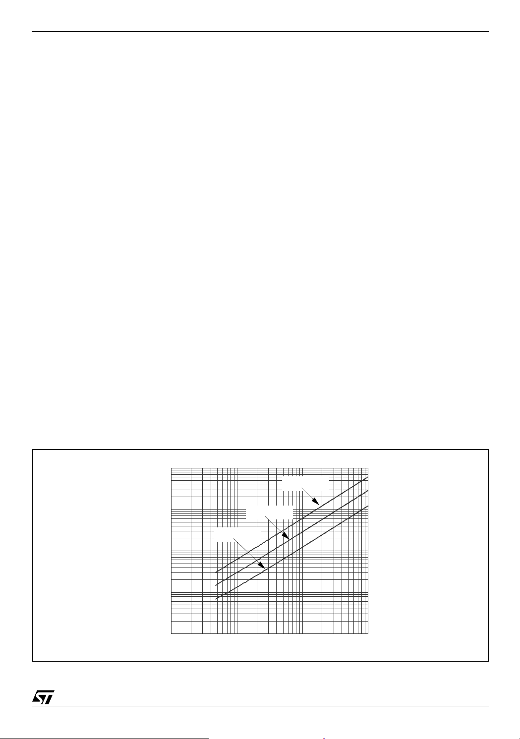
Figure 12 shows the magnitude of the Off Time t
versus C
OFF
OFF
and R
values. It can be approximately
OFF
calculated from the equations:
t
t
where R
20K
0.47nF ≤ C
t
= 0.6 · R
RCFALL
= t
OFF
RCFALL
and C
OFF
Ω ≤
= 1µs (typical value)
DT
R
OFF
OFF
OFF
· C
OFF
+ tDT = 0.6 · R
OFF
OFF
· C
OFF
+ t
DT
are the external component values and tDT is the internally generated Dead Time with:
≤ 100K
Ω
≤ 100nF
Therefore:
t
OFF(MIN)
t
OFF(MAX)
These values allow a sufficient range of t
The capacitor value chosen for C
Rise Time t
monostable is triggered. Therefore, the On Time t
be bigger than t
can not be smaller than the minimum on time t
⎧
⎨
⎩
t
RCRISE
= 6.6µs
= 6ms
will only be an issue if the capacitor is not completely charged before the next time the
RCRISE
for allowing a good current regulation by the PWM stage. Furthermore, the On Time t
RCRISE
t
>2.5µs (typ. value)=
ONtON MIN()
t
ONtRCRISEtDT
= 600 · C
–>
OFF
to implement the drive circuit for most motors.
OFF
also affects the Rise Time t
OFF
, which depends by motors and supply parameters, has to
ON
ON(MIN)
.
of the voltage at the pin RCOFF. The
RCRISE
ON
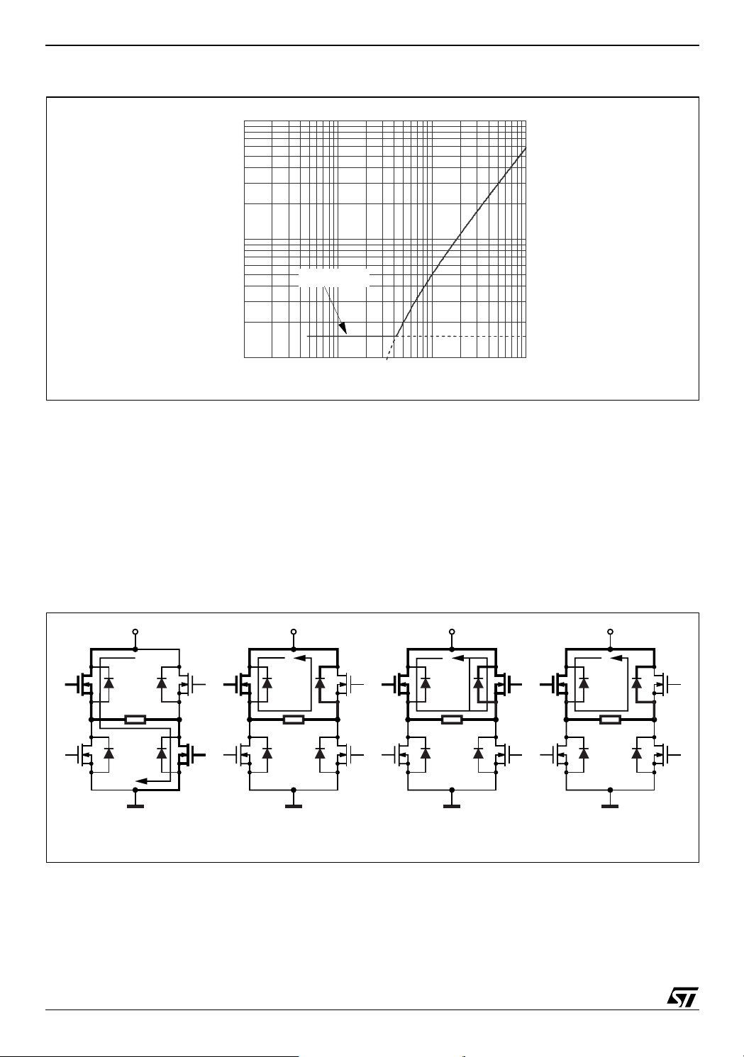
Figure 13 shows the lower limit for the On Time tON for having a good PWM current regulation capacity. It has
to be said that t
than t
RCRISE
So, small C
is always bigger than t
ON
ON(MIN)
- tDT. In this last case the device continues to work but the Off Time t
value gives more flexibility for the applications (allows smaller On Time and, therefore, higher
OFF
switching frequency), but, the smaller is the value for C
because the device imposes this condition, but it can be smaller
is not more constant.
OFF
, the more influential will be the noises on the circuit
OFF
performance.
Figure 12. t
versus C
OFF
and R
OFF
4
1.10
3
1.10
100
toff [µs]
10
1
0.1 1 10 100
OFF
.
= 100kΩ
R
off
= 47kΩ
R
off
= 20kΩ
R
off
Coff [nF]
11/25
Page 12
L6229
Figure 13. Area where tON can vary maintaining the PWM regulation.
100
10
ton(mi n) [µs]
1.5µs (typ. value)
1
0.1 1 10 10 0
3.4 SLOW DECAY MODE
Coff [nF]
Figure 14 shows the operation of the bridge in the Slow Decay mode during the Off Time. At any time only two
legs of the three-phase bridge are active, therefore only the two active legs of the bridge are shown in the figure
and the third leg will be off. At the start of the Off Time, the lower power MOS is switched off and the current
recirculates around the upper half of the bridge. Since the voltage across the coil is low, the current decays slowly. After the Dead Time the upper power MOS is operated in the synchronous rectification mode reducing the
impendence of the freewheeling diode and the related conducting losses. When the monostable times out, upper MOS that was operating the synchronous mode turns off and the lower power MOS is turned on again after
some delay set by the Dead Time to prevent cross conduction.
Figure 14. Slow Decay Mode Output Stage Configurations
A) ON TIME B) 1µs DEAD TIME C) SYNCHRONOUS
D01IN1336
RECTIFICATION
D) 1µs DEAD TIME
12/25
Page 13
L6229
3.5 DECODING LOGIC
The Decoding Logic section is a combinatory logic that provides the appropriate driving of the three-phase
bridge outputs according to the signals coming from the three Hall Sensors that detect rotor position in a 3phase BLDC motor. This novel combinatory logic discriminates between the actual sensor positions for sensors
spaced at 60, 120, 240 and 300 electrical degrees. This decoding method allows the implementation of a universal IC without dedicating pins to select the sensor configuration.
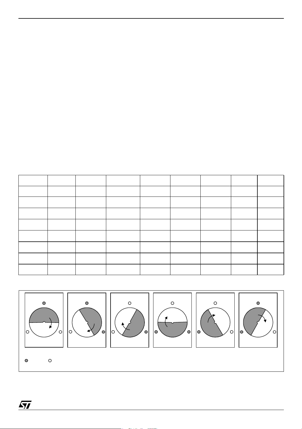
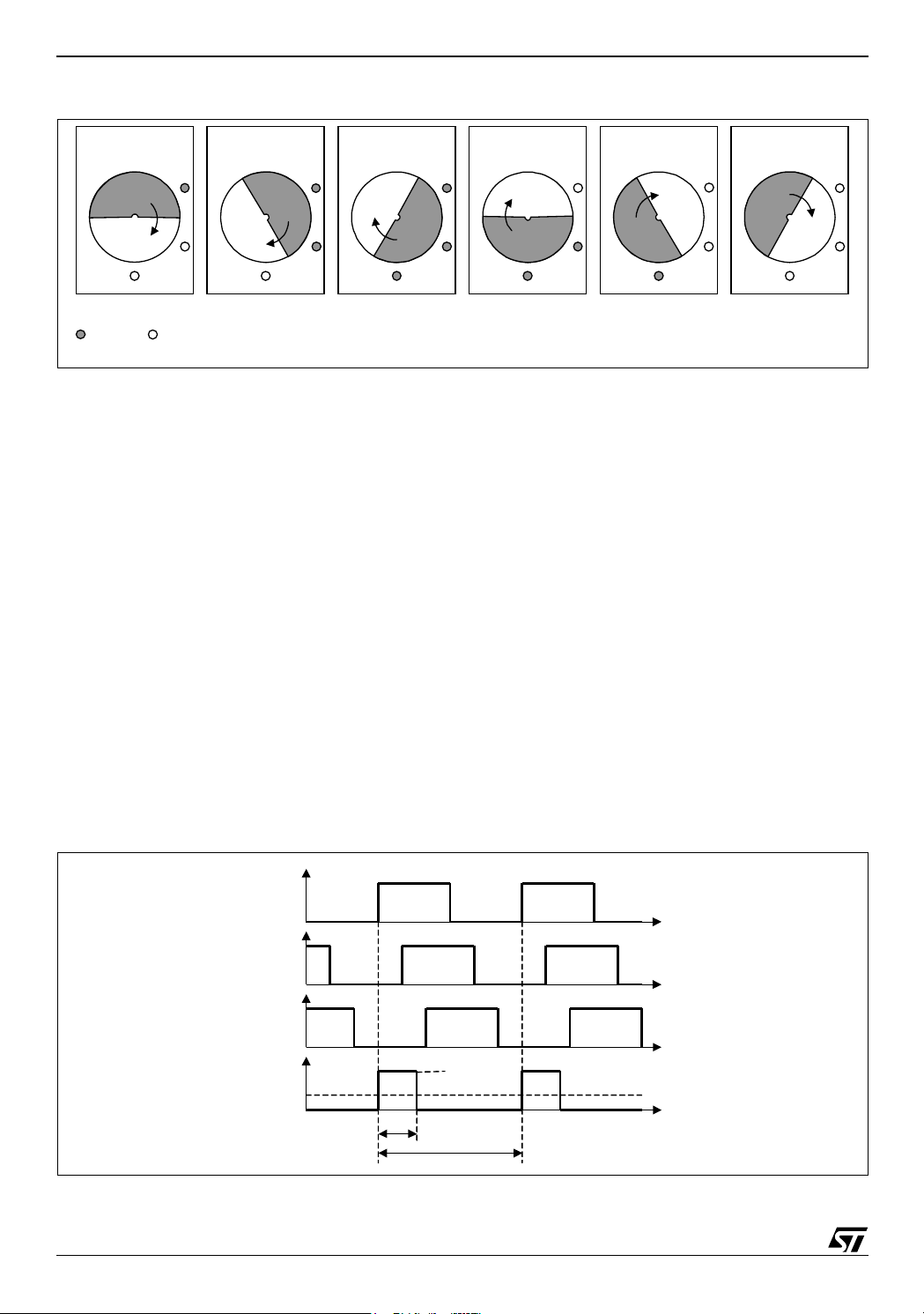
There are eight possible input combinations for three sensor inputs. Six combinations are valid for rotor positions with 120 electrical degrees sensor phasing (see Figure 15, positions 1, 2, 3a, 4, 5 and 6a) and six combinations are valid for rotor positions with 60 electrical degrees phasing (see Figure 17, positions 1, 2, 3b, 4, 5
and 6b). Four of them are in common (1, 2, 4 and 5) whereas there are two combinations used only in 120 electrical degrees sensor phasing (3a and 6a) and two combinations used only in 60 electrical degrees sensor phasing (3b and 6b).
The decoder can drive motors with different sensor configuration simply by following the Table 8. For any input
configuration (H
tion 3a is the same than 3b and analogously output configuration 6a is the same than 6b.
The sequence of the Hall codes for 300 electrical degrees phasing is the reverse of 60 and the sequence of the
Hall codes for 240 phasing is the reverse of 120. So, by decoding the 60 and the 120 codes it is possible to drive
the motor with all the four conventions by changing the direction set.
Table 8. 60 and 120 Electrical Degree Decoding Logic in Forward Direction.
Hall 120° 1 2 3a - 4 5 6a -
, H2 and H3) there is one output configuration (OUT1, OUT2 and OUT3). The output configura-
1
Hall 60° 1 2 - 3b 4 5 - 6b
H
1
H
2
H
3
OUT
1
OUT
2
OUT
3
Phasing 1->3 2->3 2->1 2->1 3->1 3->2 1->2 1->2
HH L H L LHL
LHHHHLLL
LL L HH HHL
Vs High Z GND GND GND High Z Vs Vs
High Z Vs Vs Vs High Z GND GND GND
GND GND High Z High Z Vs Vs High Z High Z
Figure 15. 120° Hall Sensor Sequence.
H1
H3 H2
H1
H2 H2 H2 H2 H2 H3 H3 H3 H3 H3
H1 H1 H1 H1
1 2 3a 4 5 6a
= H
= L
13/25
Page 14
L6229
Figure 16. 60° Hall Sensor Sequence.
H3
H1 H1
H2
H3 H3 H3 H3 H3
H2 H2 H2 H2 H2
H1 H1 H1 H1
1 2 3b 4 5 6b
= H
3.6 TACHO
A tachometer function consists of a monostable, with constant off time (t
signal (H
18. For component values refer to Application Information section.
The monostable output drives an open drain output pin (TACHO). At each rising edge of the Hall Effect Sensors
, the monostable is triggered and the MOSFET connected to pin TACHO is turned off for a constant time
H
1
(see Figure 17). The off time t
t
PULSE
to the pin RCPULSE. Figure 19 gives the relation between t
t
PULSE
where C
By connecting the tachometer pin to an external pull-up resistor, the output signal average value V
tional to the frequency of the Hall Effect signal and, therefore, to the motor speed. This realizes a simple Frequency-to-Voltage Converter. An op amp, configured as an integrator, filters the signal and compares it with a
reference voltage V
= L
), whose input is one Hall Effect
). It allows developing an easy speed control loop by using an external op amp, as shown in Figure
1
can be set using the external RC network (R
PULSE
PULSE
= 0.6 · R
should be chosen in the range 1nF … 100nF and R
PUL
· C
PUL
PUL
, which sets the speed of the motor.
REF
PUL
PULSE
, C
and C
PUL
, R
PUL
PUL
. We have approximately:
in the range 20KΩ … 100KΩ.
) connected
PUL
is propor-
M
t
PULSE
----------------- -
V
M
V
⋅=
T
DD
Figure 17. Tacho Operation Waveforms.
H1
H
2
H
3
V
TACHO
VM
14/25
t
PULSE
VDD
T
Page 15
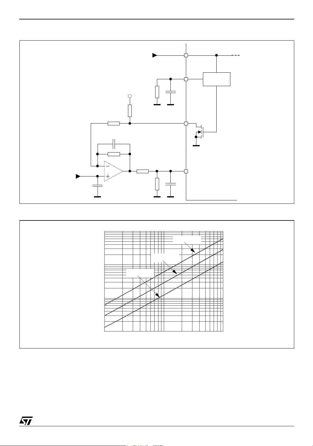
Figure 18. Tachometer Speed Control Loop.
L6229
H
1
Figure 19. t
PULSE
V
REF
versus C
PUL
1.10
C
REF2
and R
4
RCPULSE
V
DD
C
R
PUL
R
1
4
PUL
DD
R
1
R
2
.
R
3
C
R
PUL
TACHO
VREF
C
REF1
R
PUL
= 100k
MONOSTABLE
Ω
TACHO
Ω
= 47k
R
3
1.10
= 20k
R
PUL
tpulse [µs]
100
10
110100
PUL
Ω
Cpul [nF]
15/25
Page 16
L6229
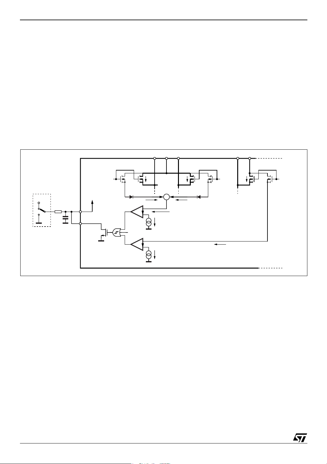
3.7 NON-DISSIPATIVE OVERCURRENT DETECTION and PROTECTION
The L6229 integrates an Overcurrent Detection Circuit (OCD) for full protection. This circuit provides Output-toOutput and Output-to-Ground short circuit protection as well. With this internal over current detection, the external current sense resistor normally used and its associated power dissipation are eliminated. Figure 20 shows
a simplified schematic for the overcurrent detection circuit.
To implement the over current detection, a sensing element that delivers a small but precise fraction of the output current is implemented with each High Side power MOS. Since this current is a small fraction of the output
current there is very little additional power dissipation. This current is compared with an internal reference current I
. When the output current reaches the detection threshold (typically I
REF
ator signals a fault condition. When a fault condition is detected, an internal open drain MOS with a pull down
capability of 4mA connected to pin DIAG is turned on.
µ
The pin DIAG can be used to signal the fault condition to a
by connecting it to pin EN and adding an external R-C (see R
C or to shut down the Three-Phase Bridge simply
, CEN).
EN
Figure 20. Overcurrent Protection Simplified Schematic
OUT
VS
OUT
1
2
A
= 2.8A) the OCD compar-
SOVER
OUT3VS
B
HIGH SIDE DMOS
I
1
µC or LOGIC
V
DD
POWER SENSE
LOGIC
DS(ON)
1 cell
INTERNAL
OPEN-DRAIN
TO GATE
R
EN
EN
C
EN
DIAG
R
40Ω TYP.
POWER DMOS
OCD
COMPARATOR
n cells
I1 / n
I1+I2 / n
I
REF
OVER TEMPERATURE
I
REF
Figure 21 shows the Overcurrent Detetection operation. The Disable Time t
HIGH SIDE DMOS HIGH SIDE DMOS
+
I
2
POWER DMOS
n cells
I2/ n
POWER SENSE
1 cell
I3/ n
D02IN1381
DISABLE
I
POWER DMOS
before recovering normal
3
POWER SENSE
n cells
1 cell
operation can be easily programmed by means of the accurate thresholds of the logic inputs. It is affected
whether by C
ing off the bridge when an overcurrent has been detected depends only by C
and REN values and its magnitude is reported in Figure 22. The Delay Time t
EN
value. Its magnitude is reported
EN
DELAY
before turn-
in Figure 23
C
is also used for providing immunity to pin EN against fast transient noises. Therefore the value of C
EN
EN
should be chosen as big as possible according to the maximum tolerable Delay Time and the REN value should
be chosen according to the desired Disable Time.
The resistor R
should be chosen in the range from 2.2KΩ to 180KΩ. Recommended values for REN and C
EN
EN
are respectively 100KΩ and 5.6nF that allow obtaining 200µs Disable Time.
16/25
Page 17
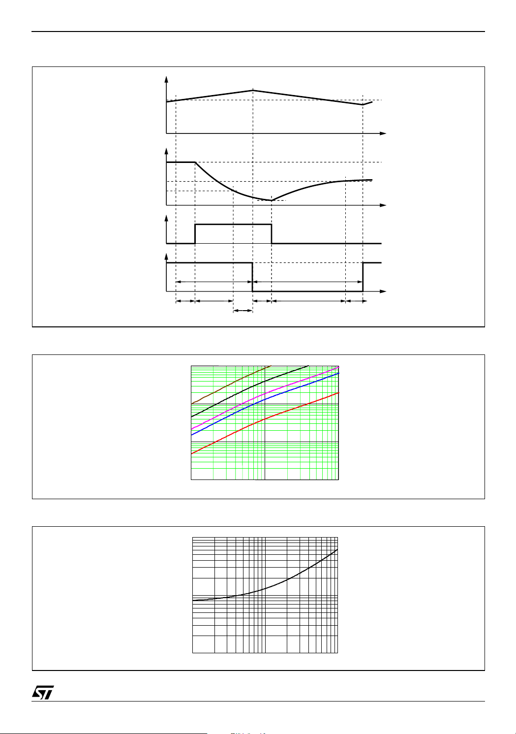
Figure 21. Overcurrent Protection Waveforms
I
OUT
I
SOVER
VEN=V
DIAG
V
DD
V
th(ON)
V
th(OFF)
ON
OCD
OFF
ON
t
BRIDGE
OFF
t
OCD(ON)
DELAY
t
EN(FALL)
t
D(OFF)EN
t
OCD(OFF)
V
EN(LOW)
t
DISABLE
t
EN(RISE)
t
D(ON)EN
L6229
D02IN1383
Figure 22. t
Figure 23. t
DISABLE
DELAY
versus CEN and REN.
3
3
1.10
1.10
100
100
[µs]
[µs]
DISABLE
DISABLE
t
t
10
10
1
1
110100
110100
versus CEN.
10
1
tdelay [µs]
REN= 220 k
REN= 220 k
CEN[nF ]
CEN[nF ]
Ω
Ω
REN= 100 k
REN= 100 k
Ω
Ω
R
R
R
R
R
R
EN
EN
EN
EN
EN
EN
= 47 k
= 47 k
= 33 k
= 33 k
= 10 k
= 10 k
Ω
Ω
Ω
Ω
Ω
Ω
0.1
110100
Cen [nF]
17/25
Page 18
L6229
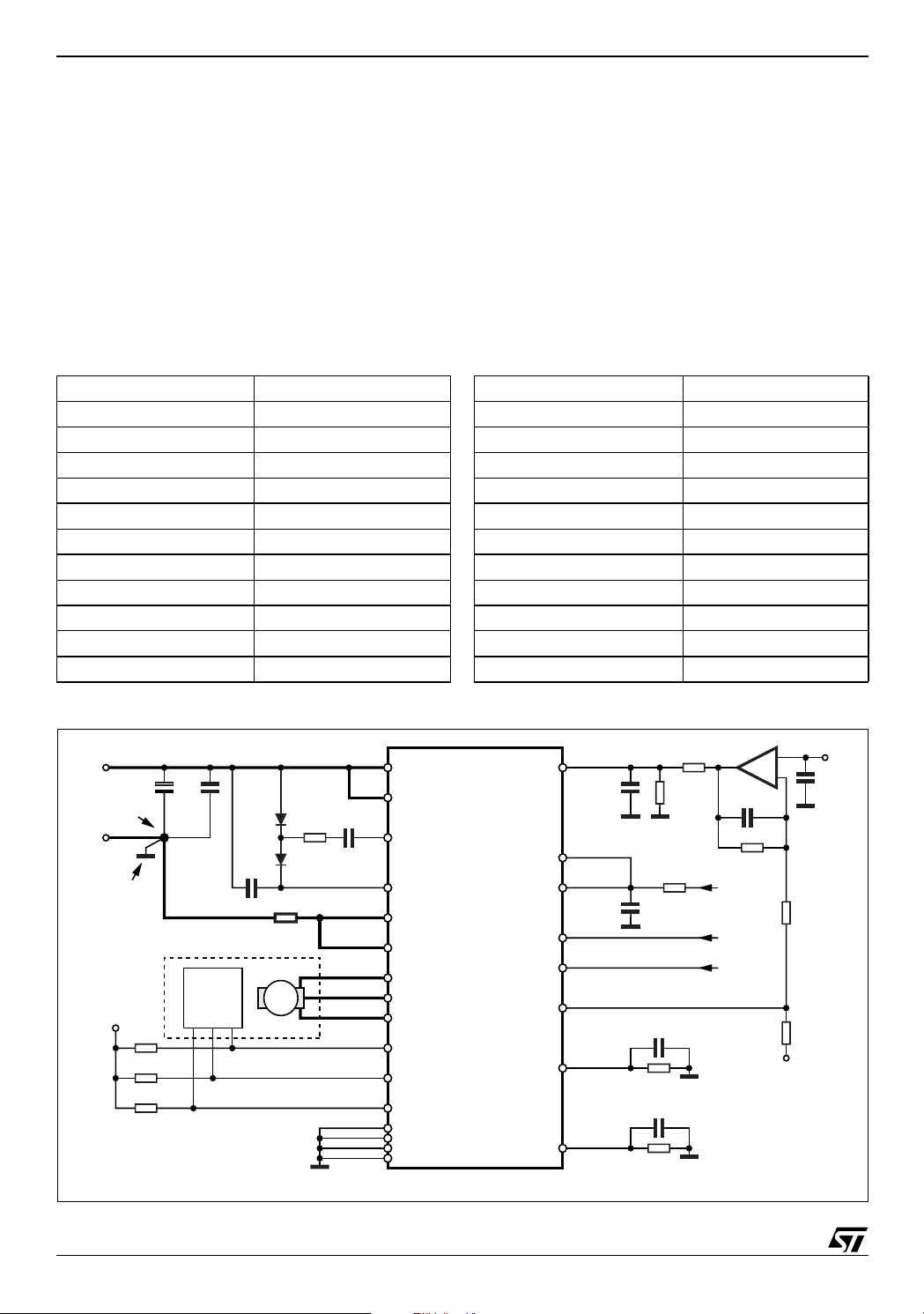
4 APPLICATION INFORMATION
A typical application using L6229 is shown in Figure 24. Typical component values for the application are shown
in Table 9. A high quality ceramic capacitor (C
power pins VS
and VSB and ground near the L6229 to improve the high frequency filtering on the power supply
A
and reduce high frequency transients generated by the switching. The capacitor (C
input to ground sets the shut down time when an over current is detected (see Overcurrent Protection). The two
current sensing inputs (SENSE
and SENSEB) should be connected to the sensing resistor R
A
length as short as possible in the layout. The sense resistor should be non-inductive resistor to minimize the di/
dt transients across the resistor. To increase noise immunity, unused logic pins are best connected to 5V (High
Logic Level) or GND (Low Logic Level) (see pin description). It is recommended to keep Power Ground and
Signal Ground separated on PCB.
Table 9. Component Values for Typical Application.
C
C
C
C
C
C
1
C
2
C
3
BOOT
OFF
PUL
REF1
REF2
C
EN
C
P
D
1
D
2
100µF R
100nF R
220nF R
220nF R
1nF R
10nF R
33nF R
100nF R
5.6nF R
10nF R
1N4148 RH1, RH2, R
1N4148
) in the range of 100nF to 200nF should be placed between the
2
) connected from the EN
EN
with a trace
SENSE
1
2
3
4
DD
EN
P
SENSE
OFF
PUL
H3
5K6Ω
1K8Ω
4K7Ω
1MΩ
1KΩ
100KΩ
100Ω
0.6Ω
33KΩ
47KΩ
10KΩ
Figure 24. Typical Application
+
V
S
C
C
1
8-52V
DC
POWER
GROUND
-
SIGNAL
GROUND
+5V
R
R
R
2
THREE-PHASE MOTOR
HALL
SENSOR
H1
H2
H3
C
BOOT
D
1
R
D
SENSE
M
VS
A
20
VS
B
17
C
P
R
P
VCP
22
2
VBOOT
SENSE
SENSE
OUT
OUT
OUT
GND
15
A
3
B
10
1
5
2
21
3
16
H
1
1
H
2
23
H
3
24
18
19
6
7
D02IN1357
VREF +
13
C
REF1
DIAG
2
EN
12
11
FWD/REV
14
BRAKE
8
TACHO
RCOFF
4
RCPULSE
9
R
1
R
2
R
EN
C
EN
C
OFF
R
OFF
C
PUL
R
PUL
C
3
R
4
ENABLE
FWD/REV
BRAKE
-
5V
V
REF
C
REF2
R
3
R
DD
18/25
Page 19
L6229
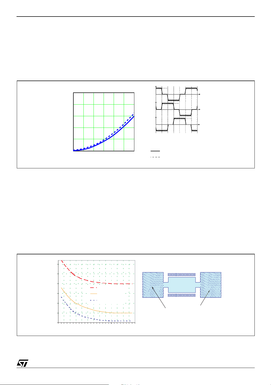
4.1 OUTPUT CURRENT CAPABILITY AND IC POWER DISSIPATION
In Figure 25 is shown the approximate relation between the output current and the IC power dissipation using
PWM current control.
For a given output current the power dissipated by the IC can be easily evaluated, in order to establish which
package should be used and how large must be the on-board copper dissipating area to guarantee a safe operating junction temperature (125°C maximum).
Figure 25. IC Power Dissipation versus Output Power.
I1
I
10
8
P
[W]
D
6
I
I
OUT
2
3
I
OUT
I
OUT
4
2
Test Condition s:
Supply Voltage = 24 V
I
OUT
[A]
No PWM
fSW = 30 kHz (slow decay)
0
0 0.25 0.5 0.75 1 1.25 1.5
4.2 THERMAL MANAGEMENT
In most applications the power dissipation in the IC is the main factor that sets the maximum current that can
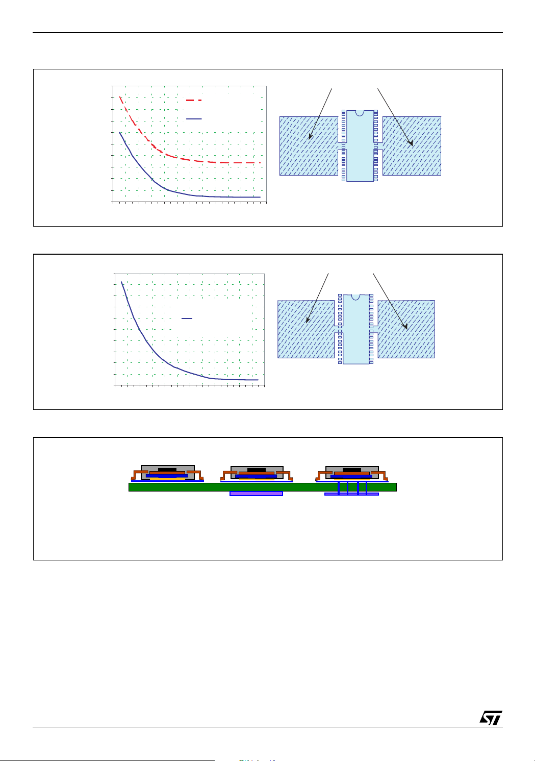
be delivered by the device in a safe operating condition. Selecting the appropriate package and heatsinking configuration for the application is required to maintain the IC within the allowed operating temperature range for
the application. Figures 26, 27 and 28 show the Junction-to-Ambient Thermal Resistance values for the
PowerSO36, PowerDIP24 and SO24 packages.
For instance, using a PowerSO package with copper slug soldered on a 1.5mm copper thickness FR4 board
with 6cm
2
dissipating footprint (copper thickness of 35µm), the R
th(j-amb)
is about 35°C/W. Figure 29 shows
mounting methods for this package. Using a multi-layer board with vias to a ground plane, thermal impedance
can be reduced down to 15°C/W.
Figure 26. PowerSO36 Junction-Ambient thermal resistance versus on-board copper area.
ºC / W
43
38
33
28
23
18
13
12345678910111213
Without Ground Layer
With Ground Layer
With Ground Layer+16 via
Holes
sq. cm
On-Board Copper Area
19/25
Page 20
L6229
Figure 27. PowerDIP24 Junction-Ambient thermal resistance versus on-board copper area.
ºC / W
49
48
47
46
45
44
43
42
41
40
39
1 2 3 4 5 6 7 8 9 101112
Copper Area is on Bottom
Side
Copper Area is on Top Side
sq. cm
On-Board Copper Area
Figure 28. SO24 Junction-Ambient thermal resistance versus on-board copper area.
ºC / W
68
66
64
62
60
58
56
54
52
50
48
123456789101112
Copper Area is on Top Side
sq. cm
On-Board Copper Area
Figure 29. Mounting the PowerSO Package.
Slug soldered
20/25
to PCB with
dissipating area
dissipating area
plus ground layer
Slug soldered
to PCB with
Slug soldered to PCB with
dissipating area plus grou nd layer
contacted through via h oles
Page 21
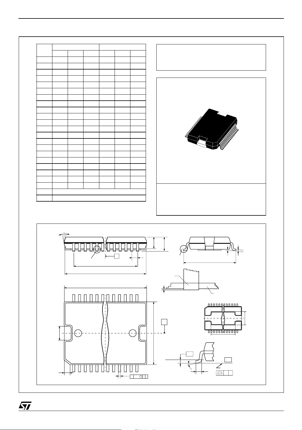
Figure 30. PowerSO36 Mechanical Data & Package Dimensions
L6229
DIM.
mm inch
MIN. TYP. MAX. MIN. TYP. MAX.
A 3.25 3.5 0.128 0.138
A2 3.3 0.13
A4 0.8 1 0.031 0.039
A5 0.2 0.008
a100.07500.003
b 0.22 0.38 0.008 0.015
c 0.23 0.32 0.009 0.012
D 15.8 16 0.622 0.630
D1 9.4 9.8 0.37 0.38
D2 1 0.039
E 13.9 14.5 0.547 0.57
E1 10.9 11.1 0.429 0.437
E2 2.9 0.114
E3 5.8 6.2 0.228 0.244
E4 2.9 3.2 0.114 1.259
e 0.65 0.026
e3 11.05 0.435
G 0 0.075 0 0.003
H 15.5 15.9 0.61 0.625
h1.10.043
L 0.8 1.1 0.031 0.043
N 10˚ (max)
s 8˚ (max)
Note: “D and E1” do not include mold flash or protus ions.
- Mold flash or protusions shall not exceed 0.15mm (0.006”)
- Critical dime nsions are "a3", "E" and "G".
OUTLINE AND
MECHANICAL DATA
PowerSO36
E2
NN
DETAIL A
118
h x 45
A
e3
H
D
1936
b
0.12 AB
a2
A
e
M
E1
DETAIL B
lead
a3
B
Gage Plane
PSO36MEC
BOTTOM VIEW
DETAIL B
0.35
S
L
DETAIL A
a1
E
slug
D1
SEATING PLANE
(COPLANARITY)
c
E3
- C -
GC
0096119 B
21/25
Page 22
L6229
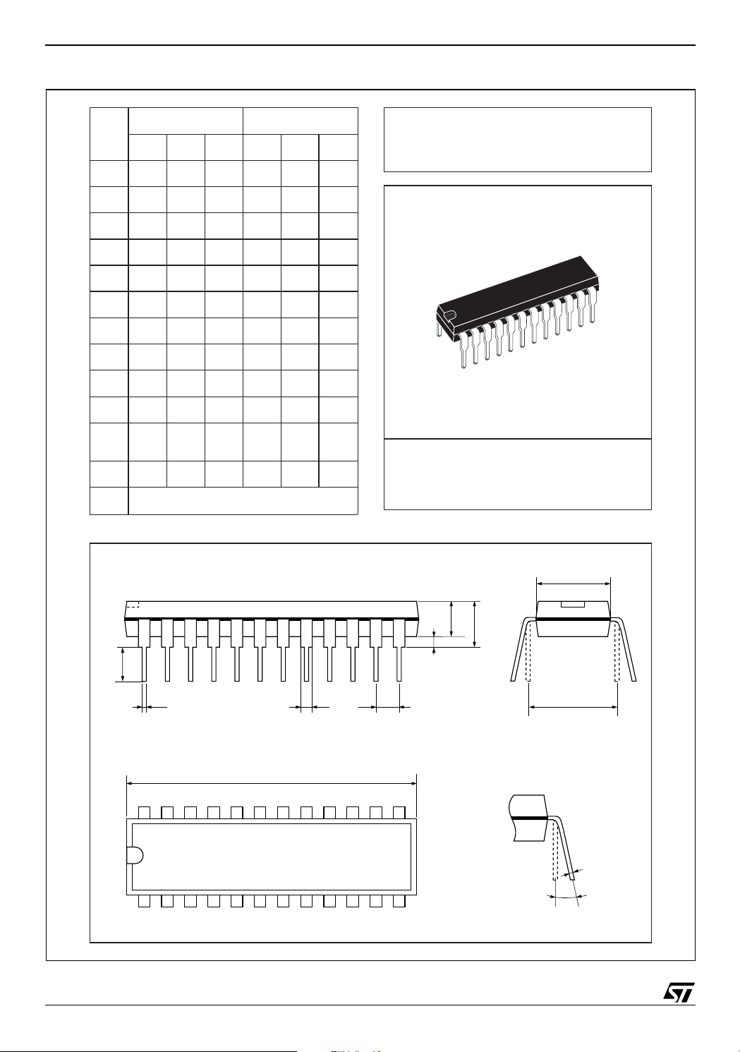
Figure 31. PDIP-24 Mechanical Data & Package Dimensions
DIM.
A 4.320 0.170
A1 0.380 0.015
A2 3.300 0.130
B 0.410 0.460 0.510 0.016 0.018 0.020
B1 1.400 1.520 1.650 0.055 0.060 0.065
c 0.200 0.250 0.300 0.008 0.010 0.012
D 31.62 31.75 31.88 1.245 1.250 1.255
E 7.620 8.260 0.300 0.325
e 2.54 0.100
E1 6.350 6.600 6.860 0.250 0.260 0.270
e1 7.620
L 3.180 3.430 0.125 0.135
M 0˚ min, 15˚ max.
mm inch
MIN. TYP. MAX. MIN. TYP. MAX.
0.300
OUTLINE AND
MECHANICAL DATA
PDIP 24 (0.300")
E1
A2
A
L
B eB1
D
24
1
A1
e1
13
c
12
SDIP24L
M
0034965 D
22/25
Page 23
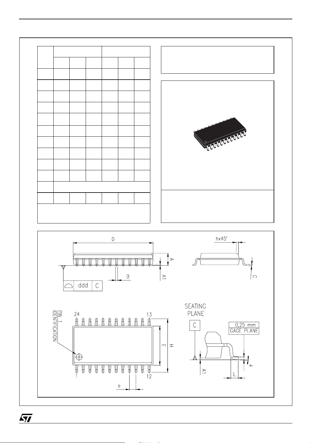
Figure 32. SO24 Mechanical Data & Package Dimensions
L6229
DIM.
A 2.35 2.65 0.093 0.104
A1 0.10 0.30 0.004 0.012
B 0.33 0.51 0.013 0.200
C 0.23 0.32 0.009 0.013
(1)
D
E 7.40 7.60 0.291 0.299
e 1.27 0.050
H 10.0 10.65 0.394 0.419
h 0.25 0.75 0.010 0.030
L 0.40 1.27 0.016 0.050
k 0˚ (min.), 8˚ (max.)
ddd 0.10 0.004
(1) “D” dimension does not include mold flash, protusions or gate
burrs. Mold flash, protus ions or gate b urrs shall not exceed
0.15mm per side.
mm inch
MIN. TYP. MAX. MIN. TYP. MAX.
15.20 15.60 0.598 0.614
OUTLINE AND
MECHANICAL DATA
Weight: 0.60gr
SO24
0070769 C
23/25
Page 24

L6229
Table 10. Revision History
Date Revision Description of Changes
September 2003 1 First Issue
January 2004 2 Migration from ST-Press dms to EDOCS.
October 2004 3 Updated the style graphic form.
24/25
Page 25

L6229
Information furnished is believed to be accurate and reliable. However, STMicroelectronics assumes no responsibility for the consequences
of use of such information nor for any infringement of patents or other rights of third parties which may result from its use. No license is granted
by implication or otherwise under any patent or patent rights of STMicroelectronics. Specifications mentioned in this publication are subject
to change without notice. This publication supersedes and replaces all information previously supplied. STMicroelectronics products are not
authorized for use as critical components in life support devices or systems without express written approval of STMicroelectronics.
The ST logo is a registered trademark of STMicroelectronics.
All other names are the property of their respective owners
© 2004 STMicroelectronics - All rights reserved
Australia - Belgium - Brazil - Canada - China - Czech Republic - Finland - France - Germany - Hong Kong - India - Israel - Italy - Japan -
Malaysia - Malta - Morocco - Singapore - Spain - Sweden - Switzerland - United Kingdom - United States of America
STMicroelectronics group of companies
www.st.com
25/25
 Loading...