

Page 1

± 625 dps full scale - 3-axis analog gyroscope
Features
■ ± 625 dps full scale
■ Wide supply voltage range 2.4 V to 3.6 V
■ Embedded power-down and sleep mode to
save power consumption and shorten turn-on
time
■ Integrated temperature sensor
■ Embedded low pass filter
■ High shock survivability
■ Extended operating temperature range (-40 °C
to 85 °C)
■ ECOPACK
Applications
®
RoHS and “Green” compliant
L3G462A
MEMS motion sensor:
Preliminary data
LGA-16
The IC interface is manufactured using a CMOS
process that allows a high level of integration to
design a dedicated circuit which is trimmed to
better match the sensing element characteristics.
The L3G462A is available in a plastic land grid
array (LGA) package and can operate within a
temperature range from -40 °C to +85 °C.
(4x4x1.1 mm)
■ Gaming and virtual reality input devices
■ Motion control with MMI (man-machine
interface)
■ GPS navigation systems
■ Appliances and robotics
Description
The L3G462A is a low-power 3-axis angular rate
sensor.
It includes a sensing element and an IC interface
able to provide the measured angular rate to the
external world through three analog outputs.
The sensing element is manufactured using a
dedicated micromachining process developed by
ST to produce inertial sensors and actuators on
silicon wafers.
Table 1. Device summary
Order code Temperature range (°C) Package Packing
L3G462A -40 to +85 LGA-16 (4x4x1.1) Tray
L3G462ATR -40 to +85 LGA-16 (4x4x1.1) Tape and reel
March 2011 Doc ID 018584 Rev 1 1/11
This is preliminary information on a new product now in development or undergoing evaluation. Details are subject to
change without notice.
www.st.com
11
Page 2

Contents L3G462A
Contents
1 Block diagram and pin description . . . . . . . . . . . . . . . . . . . . . . . . . . . . . 3
1.1 Pin description . . . . . . . . . . . . . . . . . . . . . . . . . . . . . . . . . . . . . . . . . . . . . . 3
2 Mechanical and electrical specifications . . . . . . . . . . . . . . . . . . . . . . . . 4
2.1 Mechanical characteristics . . . . . . . . . . . . . . . . . . . . . . . . . . . . . . . . . . . . . 4
2.2 Electrical characteristics . . . . . . . . . . . . . . . . . . . . . . . . . . . . . . . . . . . . . . . 5
2.3 Absolute maximum ratings . . . . . . . . . . . . . . . . . . . . . . . . . . . . . . . . . . . . . 6
2.4 Terminology . . . . . . . . . . . . . . . . . . . . . . . . . . . . . . . . . . . . . . . . . . . . . . . . 7
2.4.1 Sensitivity . . . . . . . . . . . . . . . . . . . . . . . . . . . . . . . . . . . . . . . . . . . . . . . . . 7
2.4.2 Zero-rate level . . . . . . . . . . . . . . . . . . . . . . . . . . . . . . . . . . . . . . . . . . . . . 7
2.5 Sleep mode and power-down mode . . . . . . . . . . . . . . . . . . . . . . . . . . . . . . 7
2.6 Soldering information . . . . . . . . . . . . . . . . . . . . . . . . . . . . . . . . . . . . . . . . . 7
3 Application hints . . . . . . . . . . . . . . . . . . . . . . . . . . . . . . . . . . . . . . . . . . . . 8
4 Package information . . . . . . . . . . . . . . . . . . . . . . . . . . . . . . . . . . . . . . . . . 9
5 Revision history . . . . . . . . . . . . . . . . . . . . . . . . . . . . . . . . . . . . . . . . . . . 10
2/11 Doc ID 018584 Rev 1
Page 3

L3G462A Block diagram and pin description
1 Block diagram and pin description
1.1 Pin description
Figure 1. Pin connection
+Ω
OUT_Y
X
+Ω
OUT_P
GND
Res
MS2
+Ω
OUT_R
Res
(TOP VIEW)
DIRECTIONS OF THE
DETECTABLE
ANGULAR RATES
Table 2. Pin description
Pin# Name Function
1 NC Internally not connected
2 MS1 Mode selection pin 1
VCAP
GND
13 16
12
BOTTOM
VIEW
8
Vdd
Res
Vtemp
Vdd
5
OUT_P
OUT_R
1
NC
MS1
Res
OUT_Y
49
AM09244V1
3 Res Reserved. Connect to GND
4 OUT_Y Yaw axis angular rate output
5 OUT_R Roll axis angular rate output
6 OUT_P Pitch axis angular rate output
7 Vdd Power supply
8 Res Reserved. Leave unconnected
9 Res Reserved. Leave unconnected
10 MS2 Mode selection pin 2
11 Res Reserved. Leave unconnected
12 GND 0 V supply voltage
13 GND 0 V supply voltage
14 CAP Charge pump capacitor connection pin
15 Vtemp Temperature sensor output
16 Vdd Power supply
Doc ID 018584 Rev 1 3/11
Page 4

Mechanical and electrical specifications L3G462A
2 Mechanical and electrical specifications
2.1 Mechanical characteristics
Vdd = 3.0 V, T = 25 °C unless otherwise noted
Table 3. Mechanical characteristics
Symbol Parameter Test condition Min. Typ.
FS Measurement range ±625 dps
So Sensitivity 2 mV/dps
SoDr
Zrl Zero-rate level 1.5 V
OffDr
NL Non linearity
Sensitivity change vs.
temperature
Zero-rate level change
vs. temperature
(2)
(3)
Best fit straight line 0.5 % FS
(a)
(1)
Max. Unit
±0.017 %/°C
±0.04 dps/°C
dps/
Rn Rate noise density 0.017
BW Bandwidth 140 Hz
TSo
TOff
Temperature sensor
sensitivity
Temperature sensor
offset
-2 mV/°C
27 °C 640 mV
TonPD Turn-on time From PD to normal mode 150 ms
From sleep to normal
TonSl Turn-on time
mode (no external filter
10 ms
applied)
Top
1. Typical specifications are not guaranteed.
2. Min. and max. values have been estimated based on the measurements of the current gyros in production.
3. Guaranteed by design.
Operating temperature
range
-40 +85 °C
Hz
a. The product is factory calibrated at 3.0 V. The operational power supply range is specified in Table 4.
4/11 Doc ID 018584 Rev 1
Page 5
L3G462A Mechanical and electrical specifications
2.2 Electrical characteristics
Vdd=3.0 V, T=25 °C unless otherwise noted
Table 4. Electrical characteristics
Symbol Parameter Test condition Min. Typ.
Vdd Supply voltage 2.4 3.0 3.6 V
Idd Supply current 6.9 mA
IddSL
IddPdn
To p
1. Typical specifications are not guaranteed.
2. Sleep mode introduces a faster turn-on time related to power down mode.
Supply current
in sleep mode
Supply current in
power-down mode
Operating temperature
range
(2)
Selectable by digital
interface
Selectable by digital
interface
(b)
(1)
2mA
5 µA
-40 +85 °C
Max. Unit
b. The product is factory calibrated at 3.0 V.
Doc ID 018584 Rev 1 5/11
Page 6
Mechanical and electrical specifications L3G462A
2.3 Absolute maximum ratings
Stresses above those listed as “absolute maximum ratings” may cause permanent damage
to the device. This is a stress rating only and functional operation of the device under these
conditions is not implied. Exposure to maximum rating conditions for extended periods may
affect device reliability.
Table 5. Absolute maximum ratings
Symbol Ratings Maximum value Unit
Vdd Supply voltage -0.3 to 4.8 V
T
ESD Electrostatic discharge protection 2 (HBM) kV
Storage temperature range -40 to +125 °C
STG
Sg Acceleration g for 0.1 ms 10,000 g
This is a mechanical shock sensitive device, improper handling can cause permanent
damage to the part.
This is an ESD sensitive device, improper handling can cause permanent damage to
the part.
6/11 Doc ID 018584 Rev 1
Page 7
L3G462A Mechanical and electrical specifications
2.4 Terminology
2.4.1 Sensitivity
An angular rate gyroscope is a device that produces a positive-going digital output for
counterclockwise rotation around the sensible axis considered. Sensitivity describes the
gain of the sensor and can be determined by applying a defined angular velocity to it. This
value changes very little over temperature and time.
2.4.2 Zero-rate level
Zero-rate level describes the actual output signal if there is no angular rate present. The
zero-rate level of precise MEMS sensors is, to some extent, a result of stress to the sensor
and therefore zero-rate level can slightly change after mounting the sensor onto a printed
circuit board or after exposing it to extensive mechanical stress.
2.5 Sleep mode and power-down mode
The L3G462A enables advanced power saving functionalities thanks to the different
operating modes available. When the device is set in sleep mode configuration, the reading
chain is completely turned off, allowing low power consumption. In this condition the device
turn-on time is significantly reduced allowing simple external power cycling.
The user can select the desired operating mode through two dedicated pins (MS1 and
MS2).
Table 6. Sleep mode and power-down mode configuration
Operating mode MS1 MS2
Normal mode 0 0
Power-down 1 1
Sleep mode 0 1
2.6 Soldering information
The LGA package is compliant with the ECOPACK® RoHS and “Green” standards.
It is qualified for soldering heat resistance according to JEDEC J-STD-020.
Leave “Pin 1 Indicator” unconnected during soldering.
Land pattern and soldering recommendations are available at www.st.com/mems
.
Doc ID 018584 Rev 1 7/11
Page 8
Application hints L3G462A
9nF
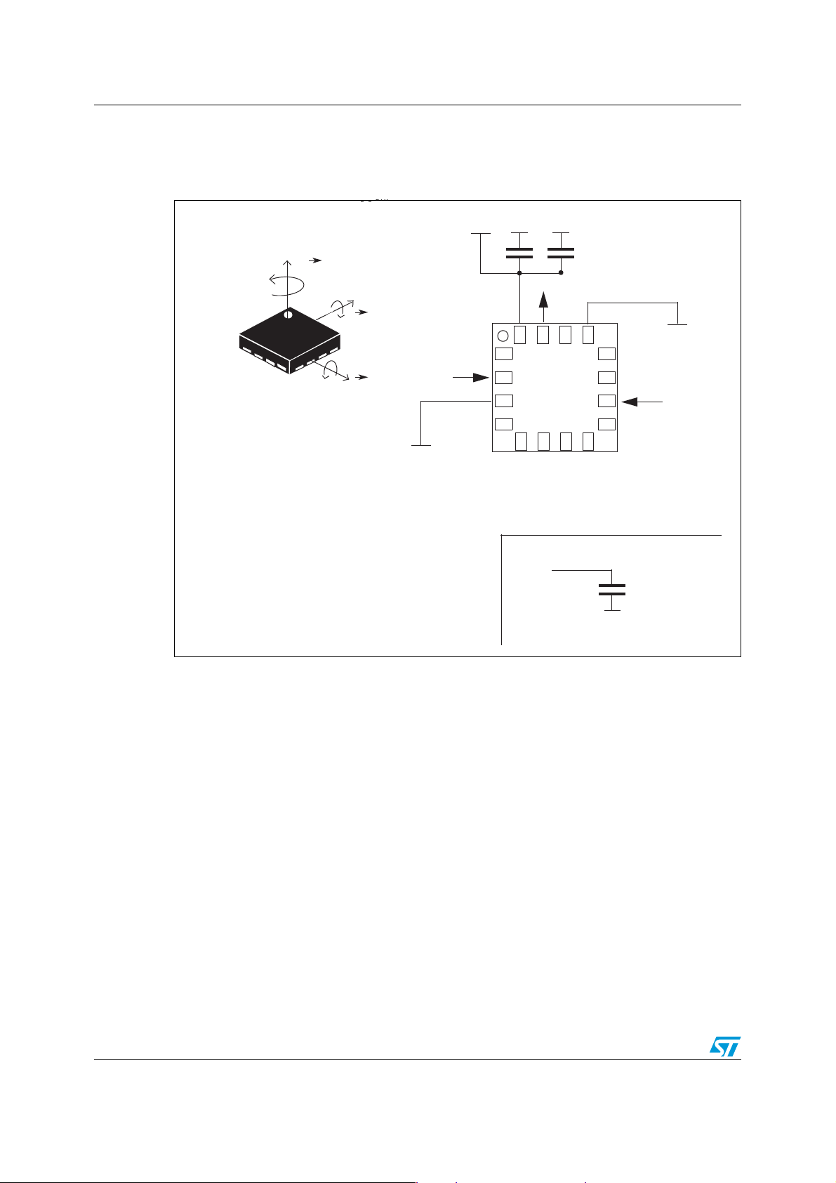
3 Application hints
Figure 2. L3G462A electrical connections and external component values
Vdd GND GND
+Ω
OUT_Y
X
(TOP VIEW)
DIRECTIONS OF THE
DETECTABLE
ANGULAR RATES
+Ω
+Ω
OUT_P
OUT_R
GND
NC
MS1
OUT_Y
Vtemp
TOP
VIEW
OUT_P
OUT_R
10 µF
CAP
Vdd
1316
12
GND
GND
Res
MS2
Res
8
Res
100 nF
Vdd
1
49
5
CAP
10 nF (25V) ±10%
GND
AM09245V1
Power supply decoupling capacitors (100 nF ceramic or polyester + 10 µF aluminum) should
be placed as near as possible to the device (common design practice). A 10 nF, 25 V class
capacitor connected to pin 14 is required for proper working of the device.
8/11 Doc ID 018584 Rev 1
Page 9
L3G462A Package information
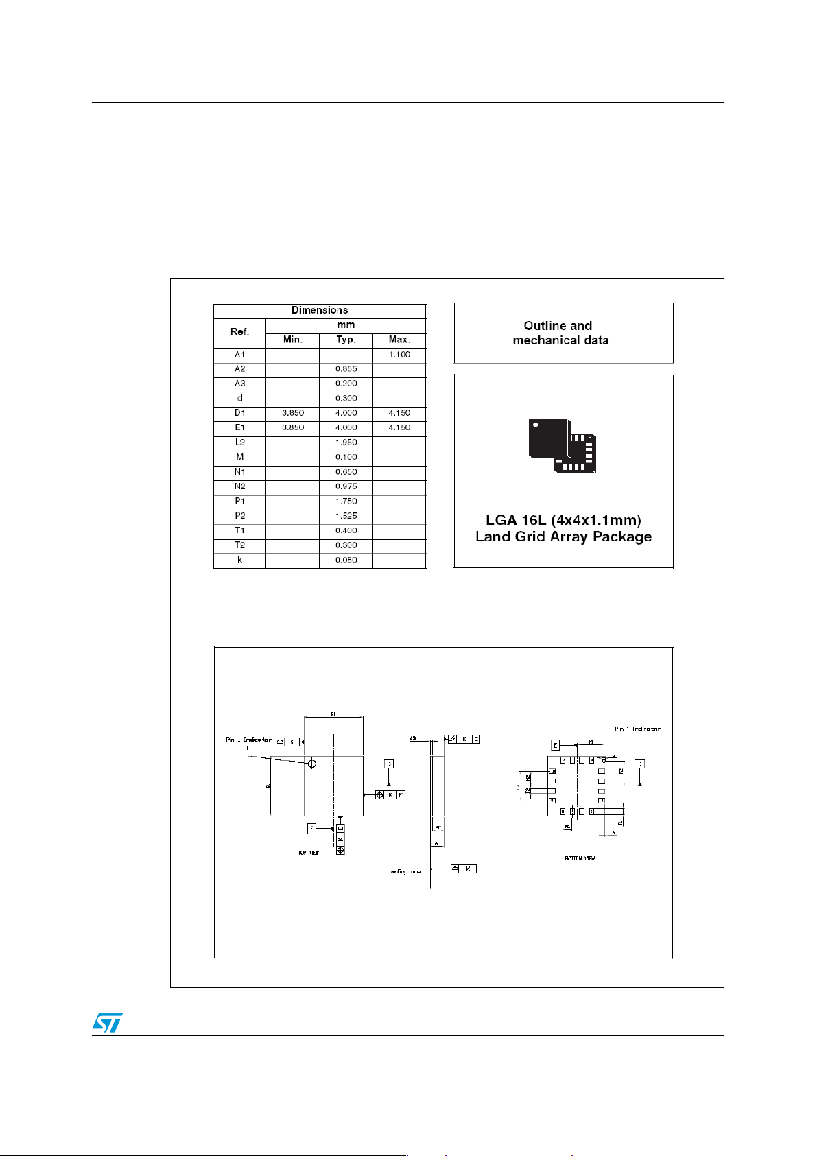
4 Package information
In order to meet environmental requirements, ST offers these devices in different grades of
ECOPACK
specifications, grade definitions, and product status are available at: www.st.com.
ECOPACK is an ST trademark.
Figure 3. LGA-16: mechanical data and package dimensions
®
packages, depending on their level of environmental compliance. ECOPACK
Doc ID 018584 Rev 1 9/11
Page 10
Revision history L3G462A
5 Revision history
Table 7. Document revision history
Date Revision Changes
15-Mar-2011 1 Initial release.
10/11 Doc ID 018584 Rev 1
Page 11

L3G462A
Please Read Carefully:
Information in this document is provided solely in connection with ST products. STMicroelectronics NV and its subsidiaries (“ST”) reserve the
right to make changes, corrections, modifications or improvements, to this document, and the products and services described herein at any
time, without notice.
All ST products are sold pursuant to ST’s terms and conditions of sale.
Purchasers are solely responsible for the choice, selection and use of the ST products and services described herein, and ST assumes no
liability whatsoever relating to the choice, selection or use of the ST products and services described herein.
No license, express or implied, by estoppel or otherwise, to any intellectual property rights is granted under this document. If any part of this
document refers to any third party products or services it shall not be deemed a license grant by ST for the use of such third party products
or services, or any intellectual property contained therein or considered as a warranty covering the use in any manner whatsoever of such
third party products or services or any intellectual property contained therein.
UNLESS OTHERWISE SET FORTH IN ST’S TERMS AND CONDITIONS OF SALE ST DISCLAIMS ANY EXPRESS OR IMPLIED
WARRANTY WITH RESPECT TO THE USE AND/OR SALE OF ST PRODUCTS INCLUDING WITHOUT LIMITATION IMPLIED
WARRANTIES OF MERCHANTABILITY, FITNESS FOR A PARTICULAR PURPOSE (AND THEIR EQUIVALENTS UNDER THE LAWS
OF ANY JURISDICTION), OR INFRINGEMENT OF ANY PATENT, COPYRIGHT OR OTHER INTELLECTUAL PROPERTY RIGHT.
UNLESS EXPRESSLY APPROVED IN WRITING BY AN AUTHORIZED ST REPRESENTATIVE, ST PRODUCTS ARE NOT
RECOMMENDED, AUTHORIZED OR WARRANTED FOR USE IN MILITARY, AIR CRAFT, SPACE, LIFE SAVING, OR LIFE SUSTAINING
APPLICATIONS, NOR IN PRODUCTS OR SYSTEMS WHERE FAILURE OR MALFUNCTION MAY RESULT IN PERSONAL INJURY,
DEATH, OR SEVERE PROPERTY OR ENVIRONMENTAL DAMAGE. ST PRODUCTS WHICH ARE NOT SPECIFIED AS "AUTOMOTIVE
GRADE" MAY ONLY BE USED IN AUTOMOTIVE APPLICATIONS AT USER’S OWN RISK.
Resale of ST products with provisions different from the statements and/or technical features set forth in this document shall immediately void
any warranty granted by ST for the ST product or service described herein and shall not create or extend in any manner whatsoever, any
liability of ST.
ST and the ST logo are trademarks or registered trademarks of ST in various countries.
Information in this document supersedes and replaces all information previously supplied.
The ST logo is a registered trademark of STMicroelectronics. All other names are the property of their respective owners.
© 2011 STMicroelectronics - All rights reserved
STMicroelectronics group of companies
Australia - Belgium - Brazil - Canada - China - Czech Republic - Finland - France - Germany - Hong Kong - India - Israel - Italy - Japan -
Malaysia - Malta - Morocco - Philippines - Singapore - Spain - Sweden - Switzerland - United Kingdom - United States of America
www.st.com
Doc ID 018584 Rev 1 11/11
 Loading...