

Page 1
HIGH OUTPUT CURRENT (4A peak)
HIGH CURRENT GAIN (10.000 typ. )
OPERA TION UP TO ± 20 V
THERMAL PROTECTION
SHOR T CIR CUIT PROTECTI O N
OPERATION WITHIN SOA
HIGH SLEW -RATE (30 V/µs)
DESCRIPTION
The L149 is a general purpose power booster in
Pentawatt ® package consisting of a quasi-complentary darlington output stage with the associated biasing system an inhibit facility.
The device is particularly suited for use wit h an operational amplifier inside a closed loop configurat ion
to increase output current.
4A LINEAR DRIVER
Pentawatt
ORDER CODE : L149V
L149
®
ABSOLUTE MAXIMUM RATINGS
Symbol Parameter Value Unit
V
s
V
V5 - V
- V
V
4
I
o
I
ο
V
INH
P
tot
i
Supply Voltage
Input Voltage V
Upper Power Transistor VCE 40 V
4
Lower Power Transistor V
3
DC Output Current 3 A
Peak Output Current (internally limited) 4 A
Input Inhibit Voltage - Vs + 5
Total Power Dissipation at T
CE
= 75 °C)
case
±20
40 V
- Vs - 1.5
25 W
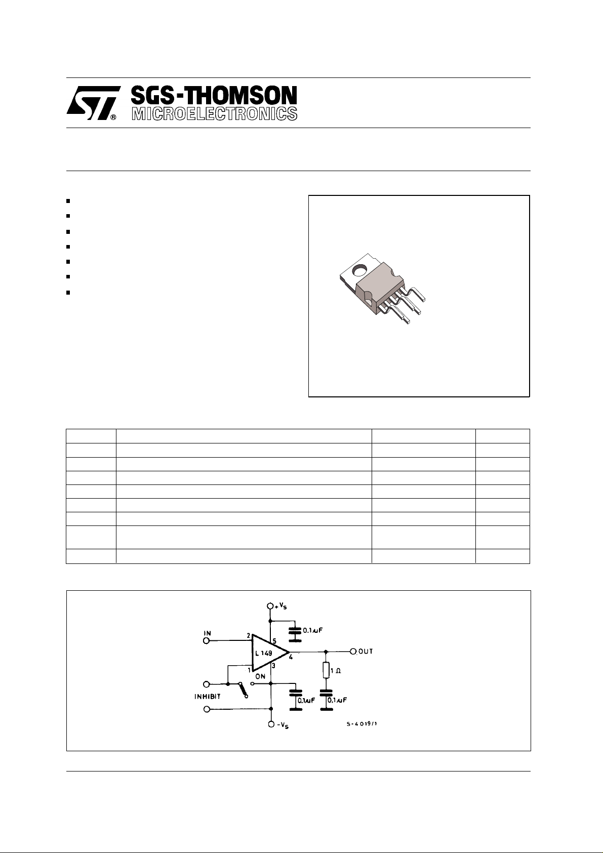
TEST CIRCUIT
V
s
V
V
March 1993
1/6
Page 2
L149
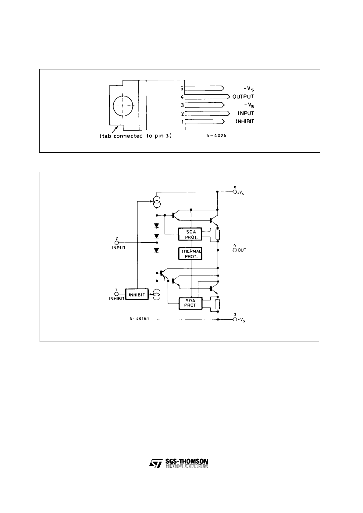
CONNECT IO N DIAG RA M (top view)
SCHEMATIC DIAGRAM
2/6
Page 3

L149
THERMAL DATA
Symbol Parameter Value Unit
Rth-j-case Thermal resistance junction-case max 3
ELECTRICAL CHARACTERISTI C S (Tj = 25 °C, Vs = ± 16V)
Symbol Parameter Test conditions Min. Typ. Max. Unit
Supply Voltage
V
s
V
V
R
I
Quiescent Drain Current
d
I
Input current
in
DC current drain
h
FE
G
Voltage gain
V
Saturation voltage
CEsat
(for each transistor)
Input offset voltage
V
os
Inhibit input voltage (pins 1-3) ON condition
INH
= ± 16 V
V
s
= ± 16 V
V
s
= ± 16 V
V
s
= ± 16 V
V
s
Io = 3A
= ± 16 V
V
s
Vi = 0V 200 400
Io = 3A 6000 10000 Io = 1.5A 1 -
0.3 V
OFF condition
Inhibit input resistance 2.0
INH
30 mA
± 1.8
SR Slew rate 30
B Power bandwidth
± 10V, d = 1%, RL = 8Ω
V
o =
200 KH
± 20
± 0.3
°C/W
3.5 V
KΩ
V/µs
V
µA
V
Z
APPLICATION INFORMATION
Figure 1. High slew-rate po wer operati o n al amp lifier (S R = 13V /µµs)
3/6
Page 4

L149
Figure 2. Maximum saturation voltage vs.
output current.
Figure 4: Supply voltage rejection vs.
frequency.
Figure 3. Current limiting characteristics.
Figure 5: Disto rsion vs. output power (f = 1KHz).
Figure 6. Disto rs i on vs. out pu t po wer
(f = 1KHz).
4/6
Figure 7. Output p ower vs. su ppl y voltage.
Page 5

PENTAWATT PACKAGE MECHANICAL DATA
DIM.
MIN. TYP. MAX. MIN. TYP. MAX.
A 4.8 0.189
C 1.37 0.054
D 2.4 2.8 0.094 0.110
D1 1.2 1.35 0.047 0.053
E 0.35 0.55 0.014 0.022
F 0.8 1.05 0.031 0.041
F1 1 1.4 0.039 0.055
G 3.4 0.126 0.134 0.142
G1 6.8 0.260 0.268 0.276
H2 10.4 0.409
H3 10.05 10.4 0.396 0.409
L 17.85 0.703
L1 15.75 0.620
L2 21.4 0.843
L3 22.5 0.886
L5 2.6 3 0.102 0.118
L6 15.1 15.8 0.594 0.622
L7 6 6.6 0.236 0.260
M 4.5 0.177
M1 4 0.157
Dia 3.65 3.85 0.144 0.152
mm inch
L149
A
H3
L
L1
C
D1
L5
Dia.
L7
L6
D
L2
L3
F1
H2
E
MM1
G1
G
F
5/6
Page 6

L149
Information furnished is believed to be accurate and reliable. However, SGS-THOMSON Microelectronics assumes no responsibility for the
consequences of use of such information nor for any infringement of pa tents or other rights of third parties which may result from its use. No
license is granted by implicat ion o r otherwise under any patent or patent rights of SGS-THOMSON Microelectronics. Specificat ions mentioned
in this publication are subject to change without notice. This publication supersedes and replaces all information previously supplied.
SGS-THOMSON Microelectroni cs products are not authorized for use as critical c omponents in life support devices or systems without express
written approval of SGS-THOMSON Microelectronics.
© 1994 SGS-THOMSON Microelectronics - A ll Rights Reserved
SGS-THOMSO N Microelec tronics G ROUP OF COMPANIES
Australia - Brazil - France - Germany - Hong Kong - Italy - Japan - Korea - Malaysia - Malta - Morocco - The Netherlands - Singapore -
Spain - Sweden - Switzerland - Taiwan - Thaliand - United Kingdom - U.S.A.
6/6
 Loading...