

Page 1
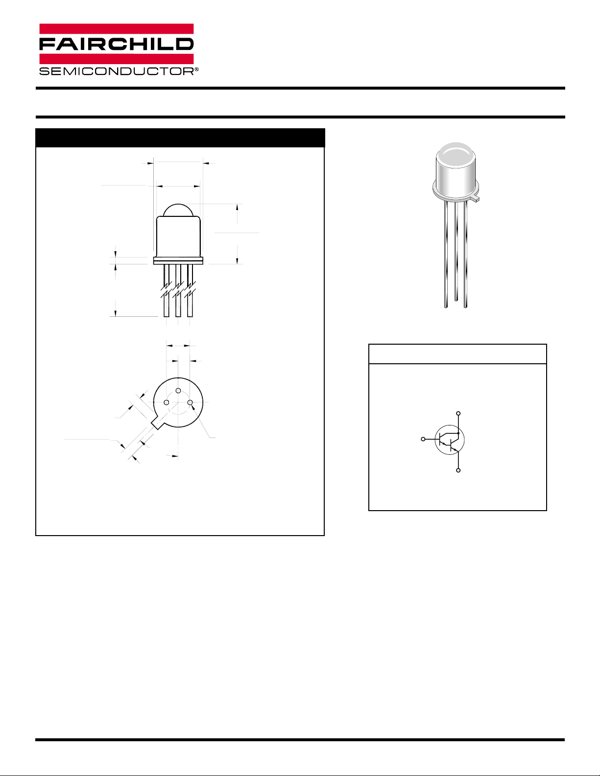
0.038 (0.97)
0.100 (2.54)
0.050 (1.27)
45°
0.046 (1.16)
0.036 (0.92)
13
0.030 (0.76)
NOM
0.195 (4.95)
0.178 (4.52)
0.230 (5.84)
0.209 (5.31)
0.500 (12.7)
MIN
0.255 (6.47)
0.225 (5.71)
Ø0.020 (0.51) 3X
2
PACKAGE DIMENSIONS
FEATURES
• Hermetically sealed package
• Narrow reception angle
NOTES:
1. Dimensions for all drawings are in inches (mm).
2. Tolerance of ± .010 (.25) on all non-nominal dimensions
unless otherwise specified.
DESCRIPTION
The L14F1/L14F2 are silicon photodarlingtons mounted in a narrow angle, TO-18 package.
2001 Fairchild Semiconductor Corporation
DS300306 6/01/01 1 OF 4 www.fairchildsemi.com
SCHEMATIC
HERMETIC SILICON
PHOTODARLINGTON
L14F1 L14F2
BASE 2
(CONNECTED TO CASE)
COLLECTOR
3
1
EMITTER
Page 2
www.fairchildsemi.com 2 OF 4 6/01/01 DS300306
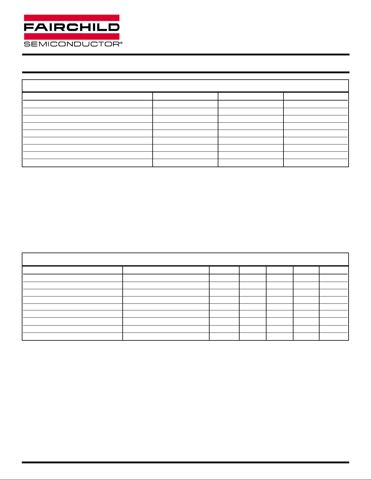
PARAMETER TEST CONDITIONS SYMBOL MIN TYP MAX UNITS
Collector-Emitter Breakdown IC= 10 mA, Ee = 0 BV
CEO
25 — V
Emitter-Base Breakdown IE= 100 µA, Ee = 0 BV
EBO
12 — V
Collector-Base Breakdown IC= 100 µA, Ee = 0 BV
CBO
25 — V
Collector-Emitter Leakage VCE= 12 V, Ee = 0 I
CEO
— 100 nA
Reception Angle at 1/2 Sensitivity θ ±8 Degrees
On-State Collector Current L14F1 Ee = .125 mW/cm2, VCE= 5 V
(7)
I
C(ON)
7.5 — mA
On-State Collector Current L14F2 Ee = .125 mW/cm2, VCE= 5 V
(7)
I
C(ON)
2.5 mA
Rise Time IC= 10 mA, VCC= 5 V, RL=100 Ω t
r
300 µs
Fall Time IC= 10 mA, VCC= 5 V, RL=100 Ω t
f
250 µs
ELECTRICAL / OPTICAL CHARACTERISTICS
(TA =25°C) (All measurements made under pulse conditions)
Parameter Symbol Rating Unit
Operating Temperature T
OPR
-65 to +125 °C
Storage Temperature T
STG
-65 to +150 °C
Soldering Temperature (Iron)
(3,4,5 and 6)
T
SOL-I
240 for 5 sec °C
Soldering Temperature (Flow)
(3,4 and 6)
T
SOL-F
260 for 10 sec °C
Collector to Emitter Breakdown Voltage
V
CEO
25 V
Collector to Base Breakdown Voltage V
CBO
25 V
Emitter to Base Breakdwon Voltage V
EBO
12 V
Power Dissipation(TA= 25°C)
(1)
P
D
300 mW
Power Dissipation(TC= 25°C)
(2)
P
D
600 mW
ABSOLUTE MAXIMUM RATINGS
(TA= 25°C unless otherwise specified)
NOTE:
1. Derate power dissipation linearly 3.00 mW/°C above 25°C ambient.
2. Derate power dissipation linearly 6.00 mW/°C above 25°C case.
3. RMA flux is recommended.
4. Methanol or isopropyl alcohols are recommended as cleaning agents.
5. Soldering iron tip
1/16” (1.6mm) minimum from housing.
6. As long as leads are not under any stress or spring tension.
7. Light source is a GaAs LED emitting light at a peak wavelength of 940 nm.
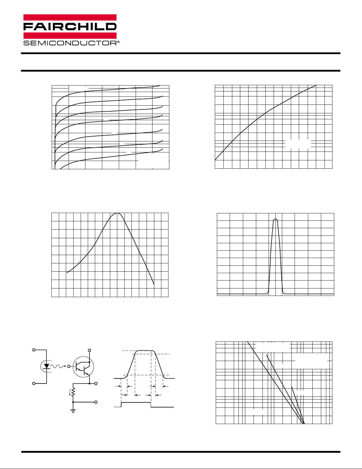
8. Figure 1 and figure 2 use light source of tungsten lamp at 2870°K color temperature. A GaAs source of 0.05 mW/cm
2
is approximately
equivalent to a tungsten source, at 2870°K, of 0.2 mW/cm
2
.
L14F1 L14F2
HERMETIC SILICON
PHOTODARLINGTON
Page 3
DS300306 6/01/01 3 OF 4 www.fairchildsemi.com
L14F1 L14F2
HERMETIC SILICON
PHOTODARLINGTON
Figure 1. Light Current vs. Collector to Emitter Voltage
100
10
1.0
, NORMALIZED LIGHT CURRENT
L
I
0.1
0
5101520253035
2
5.0 mW/cm
2.0
1.0
.5
.2
.1
.05
NORMALIZED TO:
V
Ee = .2 mW/cm
V
, COLLECTOR TO EMITTER VOLTAGE (V)
CE
CE
Figure 3. Spectral Response
1.0
0.9
0.8
0.7
0.6
0.5
0.4
0.3
0.2
RELATIVE SPECTRAL RESPONSE
0.1
0
400
600
500 900 12001000 1100
λ, WAVE LENGTH (NANOMETERS
800700
)
= 5 V
Figure 2. Relative Light Current vs. Ambient Temperature
10
8
6
4
2
1.0
.8
.6
.4
.2
.1
RELATIVE LIGHT CURRENT
.08
,
.06
°C
.04
@25
L
.02
/ I
L
2
I
.01
-50 -25 0 25
T, TEMPERATURE (
VCE = 5 V
H = .2 mW/cm
°C)
2
1251007550
Figure 4. Angular Response
110
100
90
80
70
60
50
40
RELATIVE AMPLITUDE
30
20
10
0
-70
-90
°
°
-50
-30
°
°
-10
°
DEGREES
10
°
50
°
30
°
90
°
70
°
Figure 6. Light Current vs. Relative Switching Speed
INPUT
LED56
V
LED
I
L14F
R
L
CC
OUTPUT
t
ON
1.0 V
= td + t
Figure 5. Test Circuit and Voltage Waveforms
t
d
t
r
INPUT PULSE
t
OFF
r
= ts + t
OUTPUT
PULSE
t
f
t
s
f
90%
10%
100
10
1.0
, LIGHT CURRENT (mA)
L
I
0.1
0.01 0.1 1.0 10010
LOAD RESISTANCE
10 Ω
100 Ω
VCC = 10 V
RELATIVE SWITCHING SPEED
td + tr + ts + tf
NORMALIZED TO:
RL = 100 Ω
IL = 10 mA
1000 Ω
Page 4

DISCLAIMER
FAIRCHILD SEMICONDUCTOR RESERVES THE RIGHT TO MAKE CHANGES WITHOUT FURTHER NOTICE TO
ANY PRODUCTS HEREIN TO IMPROVE RELIABILITY, FUNCTION OR DESIGN. FAIRCHILD DOES NOT ASSUME
ANY LIABILITY ARISING OUT OF THE APPLICATION OR USE OF ANY PRODUCT OR CIRCUIT DESCRIBED
HEREIN; NEITHER DOES IT CONVEY ANY LICENSE UNDER ITS PATENT RIGHTS, NOR THE RIGHTS OF
OTHERS.
LIFE SUPPORT POLICY
FAIRCHILD’S PRODUCTS ARE NOT AUTHORIZED FOR USE AS CRITICAL COMPONENTS IN LIFE SUPPORT
DEVICES OR SYSTEMS WITHOUT THE EXPRESS WRITTEN APPROVAL OF THE PRESIDENT OF FAIRCHILD
SEMICONDUCTOR CORPORATION. As used herein:
1. Life support devices or systems are devices or
systems which, (a) are intended for surgical
implant into the body,or (b) support or sustain life,
and (c) whose failure to perform when properly
used in accordance with instructions for use provided
in labeling, can be reasonably expected to result in a
significant injury of the user.
2. A critical component in any component of a life support
device or system whose failure to perform can be
reasonably expected to cause the failure of the life
support device or system, or to affect its safety or
effectiveness.
DS300306 6/01/01 4 OF 4 www.fairchildsemi.com
L14F1 L14F2
HERMETIC SILICON
PHOTODARLINGTON
 Loading...