

Page 1
2008. 2. 25 1/5
SEMICONDUCTOR
TECHNICAL DATA
KMB2D0N60SA
N-Ch Trench MOSFET
Revision No : 1
General Description
This Trench MOSFET has better characteristics, such as fast switching
time, low on resistance, low gate charge and excellent avalanche
characteristics. It is mainly suitable for portable equipment.
FEATURES
V
DSS
=60V, ID=2A
Drain-Source ON Resistance
R
DS(ON)
=160m (Max.) @ VGS=10V
R
DS(ON)
=220m (Max.) @ VGS=4.5V
Super High Dense Cell Design
MAXIMUM RATING (Ta=25 )
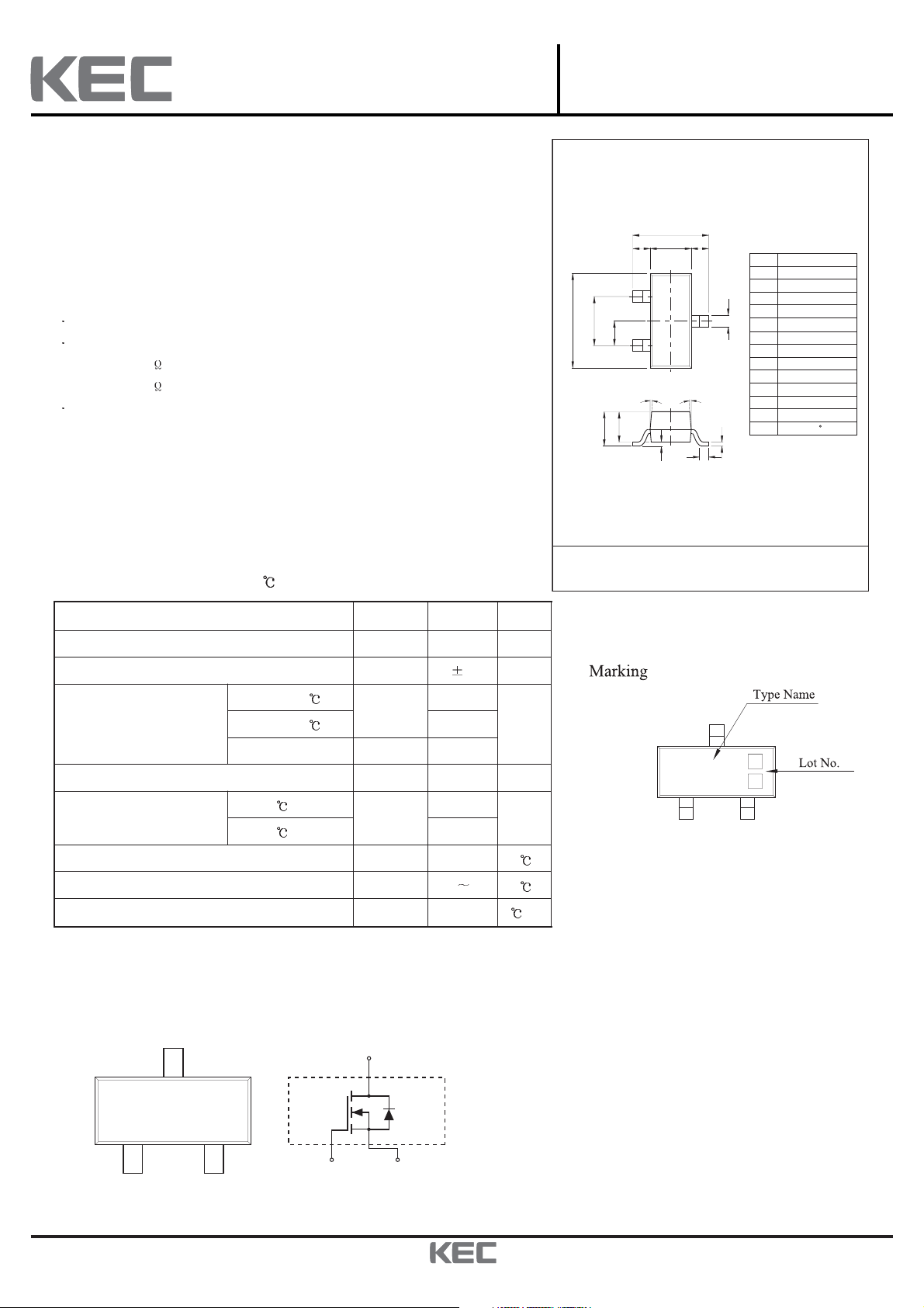
PIN CONNECTION (TOP VIEW)
CHARACTERISTIC SYMBOL N-Ch UNIT
Drain-Source Voltage
V
DSS
60 V
Gate-Source Voltage
V
GSS
20
V
Drain Current
DC@Ta=25
I
D
2.0
A
DC@Ta=70
1.6
Pulsed
I
DP
10
Drain-Source-Diode Forward Current
I
S
1.0 A
Drain Power Dissipation
Ta=25
P
D
1.25
W
Ta=70
0.8
Maximum Junction Temperature
T
j
150
Storage Temperature Range
T
stg
-55 150
Thermal Resistance, Junction to Ambient
R
thJA
100
/W
Note>*Surface Mounted on 1” × 1” FR4 Board, t≤5sec
E
B
LL
DIM MILLIMETERS
A
B
C
A
G
2
H
1
PP
N
C
M
K
D
3
D
E
G1.90
H
J
K
L
M
N
P7
J
_
+
2.93 0.20
1.30+0.20/-0.15
1.30 MAX
0.40+0.15/-0.05
2.40+0.30/-0.20
0.95
0.13+0.10/-0.05
0.00 ~ 0.10
0.55
0.20 MIN
1.00+0.20/-0.10
SOT-23
KND
D
3
2
1
3
2
1
GS
Page 2
2008. 2. 25 2/5
KMB2D0N60SA
Revision No : 1
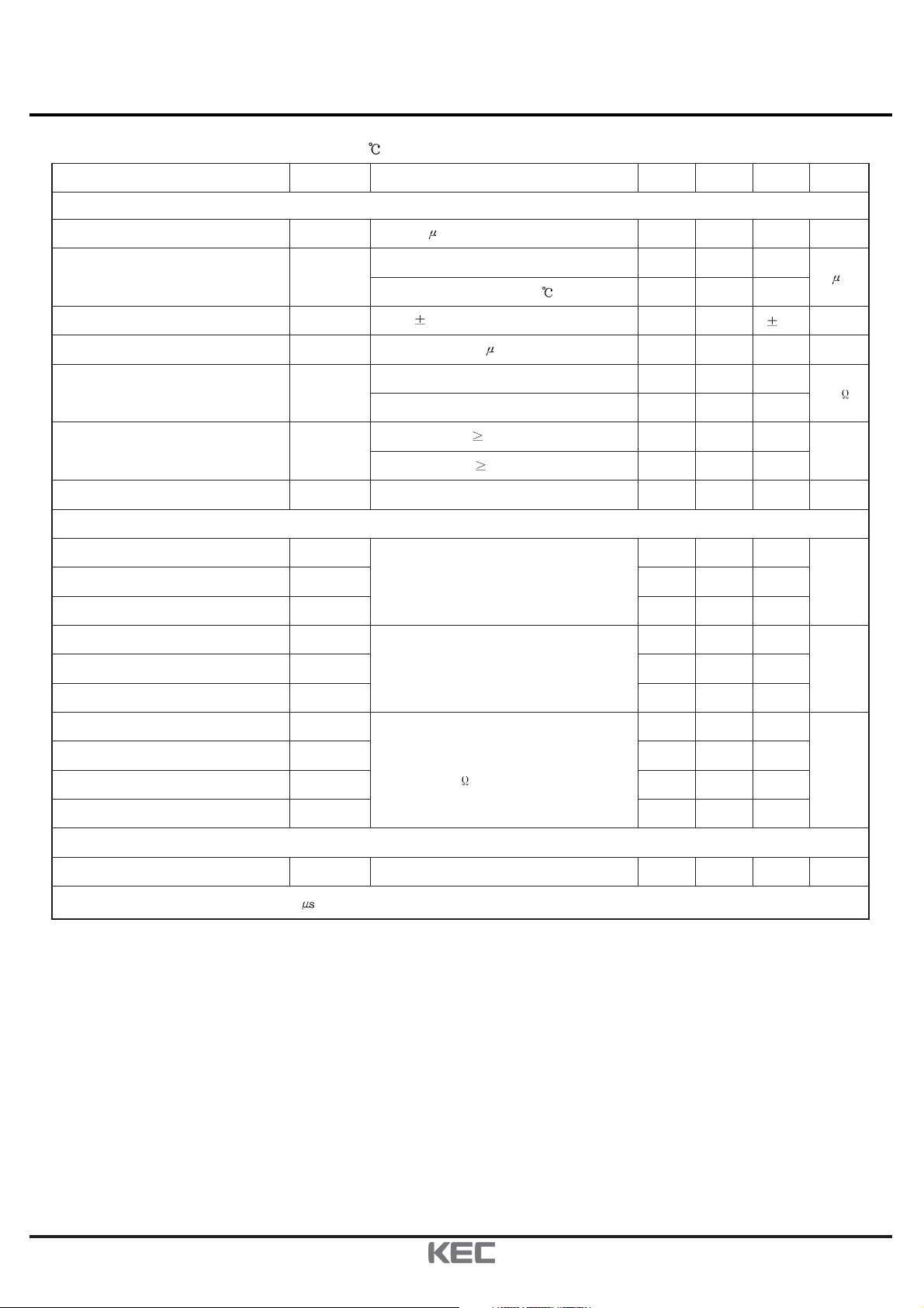
ELECTRICAL CHARACTERISTICS (Ta=25 )
CHARACTERISTIC SYMBOL TEST CONDITION MIN. TYP. MAX. UNIT
Static
Drain-Source Breakdown Voltage
BV
DSS
IDS=250 A, VGS=0V,
60 - - V
Drain Cut-off Current
I
DSS
VGS=0V, VDS=60V
- - 0.5
A
VGS=0V, VDS=60V, Tj=55
- - 10
Gate Leakage Current
I
GSS
VGS= 20V, VDS=0V
- -
100
nA
Gate Threshold Voltage
V
th
VDS=V
GS, ID
=250 A
1.5 - - V
Drain-Source ON Resistance
R
DS(ON)
*
VGS=10V, ID=2A
- 125 160
m
VGS=4.5V, ID=1.7A
- 155 220
On-State Drain Current
I
D(ON)
*
VGS=10V, VDS4.5V
6 - -
A
VGS=4.5V, VDS4.5V
4 - -
Forward Transconductance
gfs* VDS=4.5V, ID=2.0A
- 4.6 - S
Dynamic
Input Capaclitance
C
iss
VDS=30V, f=1MHz, VGS=0V
- 240 -
pFOuput Capacitance
C
oss
- 30 -
Reverse Transfer Capacitance
C
rss
- 16 -
Total Gate Charge
Qg*
VDS=30V, VGS=10V, ID=2A
- 4.8 10
nCGate-Source Charge
Qgs*
- 0.8 -
Gate-Drain Charge
Qgd*
- 1.0 -
Turn-On Delat Time
t
d(on)
*
VDD=30V, VGS=4.5V
I
D
=1A, RG=6
- 7 15
ns
Turn-On Rise Time
tr*
- 10 20
Turn-Off Deley Time
t
d(off)
*
- 17 35
Turn-Off Fall Time
tf*
- 6 15
Source-Drain Diode Ratings
Source-Drain Forward Voltage
V
SDF
* VGS=0V, IS=1A
- 0.77 1.2 V
NOTE 1> * Pulse Test : Pulse width <300 , Duty cycle < 2%
Page 3

2008. 2. 25 3/5
KMB2D0N60SA
Revision No : 1
10
10V
8
(A)
D
6
4
Drain Current I
2
0
10
Common Source
VDS=5V
Pulse Test
8
(A)
D
6
Fig1. I
5.0V
2468100
D
- V
DS
Common Source
Ta=25
Pulse Test
Drain - Source Voltage VDS (V)
Fig3. I
D
- V
GS
C
VGS=3V
4.5V
4.0V
3.5V
Fig2. R
500
(mΩ)
Source On Resistance R
Drain
DS(ON)
400
300
200
100
Common Source
Ta=25
Pulse Test
0
0
C
VGS=4.5V
4
Drain - Current ID (A)
Fig4. R
250
200
DS(ON)
150
Common Source
=10V, ID=2A
V
GS
Pulse Test
(mΩ)
DS(ON)
VGS=10V
- I
D
81216
DS(ON)
- T
j
4
Drain Current I
2
0
01
Gate-Source Volatage VGS (V)
Fig5. V
5
Common Source
VGS=V
(V)
th
4
3
2
1
Gate Threshold Voltage V
0
DS
I
=250µA
D
Pulse Test
-75 -50 -25 0 50 10075 125 15025
25
C
125
C
2345
- T
th
j
-55
C
100
50
Source On-Resistance R
0
Drain-
-25 15050 75 100 12525-50 0-75
Junction Temperature Tj ( )
10
8
(A)
S
6
4
Drain Current I
2
0
C
Fig6. IS-V
0.8 1.200.4 1.62.0
SDF
Common Source
C
Ta=25
Pulse Test
Junction Temperature Tj ( )
C
Source - Drain Forward Voltage V
SDF
(V)
Page 4

2008. 2. 25 4/5
KMB2D0N60SA
Revision No : 1
10
VDS=30V
=2.0A
I
(V)
D
8
GS
6
4
2
Gate - Source Voltage V
0
0
1
Total Gate - Charge
Fig7. V
2
- Q
GS
g
Qg (nC)
100.0
10.0
(A)
D
1.0
0.1
Drain Current I
0.01
R
Limited
DS(ON)
VGS= 10V
SINGLE PULSE
T
a
= 25 C
0.1
400
300
200
100
Capacitance C (pF)
0
543
Fig9. Safe Operation Area
110100
C
iss
C
oss
C
rss
Fig8. C - V
DS
VGS=0V
f = 1MHz
06121824 30
Drain - Source Voltage V
100µs
1ms
10ms
100ms
1s
DC
DS
(V)
1
D = 0.5
0.2
0.1
0.1
0.05
0.02
THERMAL RESISTANCE
NORMALIZED TRANSIENT
0.01
10
Single pulse
-4
10
Drain - Source Voltage V
(V)
DS
Fig10. Transient Thermal Response Curve
P
DM
- Duty = t/T
-3
-2
10
-1
10
0
10
10 10
TIME t (sec)
t
1
t
2
2
500
Page 5

2008. 2. 25 5/5
KMB2D0N60SA
Revision No : 1
Fig11. Gate Charge Circuit and Wave Form
Schottky
1.0 mA
Diode
V
GS
0.5 V
DSS
I
D
V
GS
10 V
I
D
V
DS
Q
gs
Q
gd
Q
g
Q
Fig12. Resistive Load Switching
0.5 V
DSS
6Ω
10 V
V
R
L
V
DS
V
GS
DS
V
GS
10%
t
d(on)
90%
t
t
r
t
on
d(off)
t
f
t
off
Page 6

 Loading...