

Page 1
Features
■
136µA supply current
■
4.9MHz bandwidth
■
Output swings to within 20mV of either rail
■
Input voltage range exceeds the rail by >250mV
■
5.3V/µs slew rate
■
35mA short circuit output current
■
24nV/√Hz input voltage noise
■
Directly replaces LMC7101 in single supply
applications
■
Available in SOT23-5 package
Applications
■
Portable/battery-powered applications
■
PCMCIA, USB
■
Mobile communications, cellular phones, pagers
■
Notebooks and PDA’s
■
Sensor Interface
■
A/D buffer
■
Active filters
■
Signal conditioning
■
Portable test instruments
General Description
The KM7101 is an ultra-low cost, low power, voltage
feedback amplifier that is pin compatible to the
LMC7101. If a standard pinout is required, use the
KM4170. The KM7101 uses only 136µA of supply
current and offers no crossover distortion. The input
common mode voltage range exceeds the negative
and positive rails.
The KM7101 offers high bipolar performance at a
low CMOS price. The KM7101 offers superior
dynamic performance with a 4.9MHz small signal
bandwidth and 5.3V/µs slew rate. The combination
of low power, high bandwidth, and rail-to-rail performance make the KM7101 well suited for batterypowered communication/computing systems.
KM7101
Ultra-Low Cost, 139µA, +2.7V, 4.9MHz Rail-to-Rail I/O Amplifier
www.fairchildsemi.com
REV. 1B March 2001
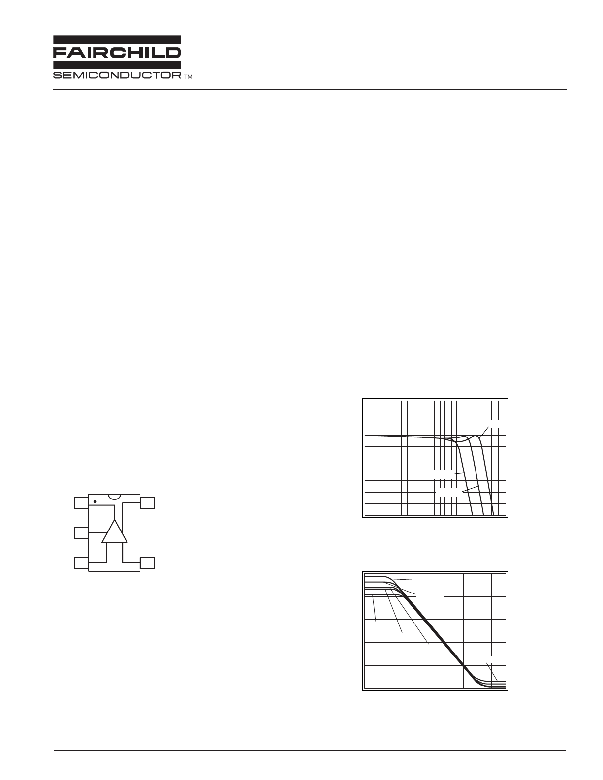
KM7101 Package
SOT23-5
Large Signal Frequency Response
Vs = 5V
Vo = 1V
pp
1
Out
+V
2
+In
s
3
-
+
Vo = 4V
pp
Magnitude (1dB/div)
-V
5
s
0.01
Frequency (MHz)
4
-In
Output Swing vs. Load
1.35
RL = 75Ω
0
Output Voltage (0.27V/div)
-1.35
RL = 100Ω
-2.0
Input Voltage (0.4V/div)
0.1
RL = 10kΩ
RL = 1kΩ
RL = 200Ω
Vo = 2V
0
pp
1
RL = 75/100Ω
10
2.0
Page 2
DATA SHEET KM7101
2 REV. 1B March 2001
Parameters Conditions TYP Min & Max UNITS NOTES
Case Temperature +25°C +25°C
Frequency Domain Response
-3dB bandwidth G = +1, Vo= 0.02V
pp
4.9 MHz 1
G = +2, Vo= 0.2V
pp
3.7 MHz
full power bandwidth G = +2, Vo= 2V
pp
1.4 MHz
gain bandwidth product 2.2 MHz
Time Domain Response
rise and fall time 1V step 163 ns
overshoot 1V step <1 %
slew rate 1V step 5.3 V/µs
Distortion and Noise Response
2nd harmonic distortion 1Vpp, 10kHz -75 dBc
3rd harmonic distortion 1Vpp, 10kHz -76 dBc
THD 1Vpp, 10kHz 0.03 %
input voltage noise >1MHz 24 nV/√Hz
DC Performance
input offset voltage 0.5 ±6 mV 2
average drift 5 µV/°C
input bias current 90 220 nA 2
average drift 32 pA/°C
power supply rejection ratio DC 83 55 dB 2
open loop gain RL= 10kΩ 90 dB
quiescent current 136 190 µA2
Input Characteristics
input resistance 12 MΩ
input capacitance 2 pF
input common mode voltage range -0.25 to 2.95 V
common mode rejection ratio DC, Vcm= 0V to V
s
81 55 dB 2
Output Characteristics
output voltage swing RL= 10kΩ to Vs/2 0.02 to 2.68 0.06 to 2.64 V 2
RL= 1kΩ to Vs/2 0.05 to 2.63 V
RL= 200Ω to Vs/2 0.11 to 2.52 V
output current ±16 mA
short circuit output current ±35 mA
power supply operating range 2.7 2.5 to 5.5 V
Min/max ratings are based on product characterization and simulation. Individual parameters are tested as noted. Outgoing quality levels
are determined from tested parameters.
NOTES:
1) For G = +1, Rf= 0.
2) 100% tested at +25°C.
Absolute Maximum Ratings Package Thermal Resistance
supply voltage 0 to +6V
Package θ
JA
maximum junction temperature +175°C
5 lead SOT23 256°C/W
storage temperature range -65°C to +150°C
lead temperature (10 sec) +300°C
operating temperature range (recommended) -40°C to +85°C
input voltage range +V
s
+ 0.5V, -Vs - 0.5V
internal power dissipation see power derating curves
KM7101 Electrical Characteristics
(Vs= +2.7V, G = 2, RL= 10kΩ to Vs/2, Rf= 5kΩ; unless noted)
Page 3
KM7101 DATA SHEET
REV. 1B March 2001 3
Parameters Conditions TYP Min & Max UNITS NOTES
Case Temperature +25°C +25°C
Frequency Domain Response
-3dB bandwidth G = +1, Vo= 0.02V
pp
4.3 MHz 1
G = +2, Vo= 0.2V
pp
3.0 MHz
full power bandwidth G = +2, Vo= 2V
pp
2.3 MHz
gain bandwidth product 2.0 MHz
Time Domain Response
rise and fall time 1V step 110 ns
overshoot 1V step <1 %
slew rate 1V step 9 V/µs
Distortion and Noise Response
2nd harmonic distortion 2Vpp, 10kHz -73 dBc
3rd harmonic distortion 2Vpp, 10kHz -75 dBc
THD 2Vpp, 10kHz 0.03 %
input voltage noise >1MHz 27 nV/√Hz
DC Performance
input offset voltage 1.5 ±8 mV 2
average drift 15 µV/°C
input bias current 90 270 nA 2
average drift 40 pA/°C
power supply rejection ratio DC 60 40 dB 2
open loop gain RL= 10kΩ 80 dB
quiescent current 160 235 µA2
Input Characteristics
input resistance 12 MΩ
input capacitance 2 pF
input common mode voltage range -0.25 to 5.25 V
common mode rejection ratio DC, Vcm= 0V to V
s
85 58 dB 2
Output Characteristics
output voltage swing RL= 10kΩ to Vs/2 0.04 to 4.96 0.08 to 4.92 V 2
RL= 1kΩ to Vs/2 0.07 to 4.9 V
RL= 200Ω to Vs/2 0.14 to 4.67 V
output current ±30 mA
short circuit output current ±60 mA
power supply operating range 5.0 2.5 to 5.5 V
Min/max ratings are based on product characterization and simulation. Individual parameters are tested as noted. Outgoing quality levels
are determined from tested parameters.
NOTES:
1) For G = +1, Rf= 0.
2) 100% tested at +25°C.
KM7101 Electrical Characteristics
(Vs= +5V, G = 2, RL= 10kΩ to Vs/2, Rf= 5kΩ; unless noted)
Page 4

KM7101 Performance Characteristics
(Vs= +2.7, G = 2, RL= 10kΩ to Vs/2, Rf= 5kΩ; unless noted)
DATA SHEET KM7101
4 REV. 1B March 2001
Non-Inverting Freq. Response Vs = +5V
Vo = 0.2V
pp
G = 2
Rf = 5kΩ
G = 10
Rf = 5kΩ
G = 5
Rf = 5kΩ
Normalized Magnitude (1dB/div)
0.01
0.1
Frequency (MHz)
Non-Inverting Freq. Response Vs = +2.7V
Vo = 0.2V
pp
G = 2
Rf = 5kΩ
G = 10
Rf = 5kΩ
G = 5
Rf = 5kΩ
1
G = 1
Rf = 0
Rf = 0
10
G = 1
Inverting Frequency Response Vs = +5V
Vo = 0.2V
pp
G = -2
Rf = 5kΩ
G = -10
Rf = 5kΩ
G = -5
R
= 5kΩ
f
Normalized Magnitude (1dB/div)
0.01
0.1
Frequency (MHz)
Inverting Frequency Response Vs = +2.7V
Rf = 5kΩ
G = -2
G = -10
G = -5
G = -1
R
= 5kΩ
f
1
10
G = -1
Normalized Magnitude (1dB/div)
0.01
0.1
1
Frequency (MHz)
Frequency Response vs. C
Vo = 0.05V
+
Magnitude (1dB/div)
-
5kΩ
0.01
CL = 100pF
= 100Ω
R
s
CL = 20pF
R
s
C
R
L
5kΩ
L
0.1
= 0
R
s
CL = 10pF
L
= 0
R
s
1
Frequency (MHz)
Large Signal Frequency Response
Vs = 5V
Vo = 4V
pp
Magnitude (1dB/div)
0.01
0.1
Vo = 2V
pp
1
Frequency (MHz)
CL = 50pF
= 0Ω
R
s
Vo = 1V
Normalized Magnitude (1dB/div)
10
0.01
0.1
1
10
Frequency (MHz)
Frequency Response vs. R
RL = 1kΩ
RL = 200Ω
Magnitude (1dB/div)
10
0.01
RL = 50Ω
0.1
1
L
RL = 10kΩ
10
Frequency (MHz)
Open Loop Gain & Phase vs. Frequency
140
|Gain|
RL = 10kΩ
pp
120
100
|Gain|
No load
Vs = 5V
Open Loop Phase (deg)
80
8
0
-45
-90
-135
-180
60
40
20
Open Loop Gain (dB)
0
Phase
RL = 10kΩ
Phase
No load
-20
10
10010110210310410510610710
Frequency (Hz)
Page 5

KM7101 Performance Characteristics
(Vs= +2.7V, G = 2, RL= 10kΩ to Vs/2, Rf= 5kΩ; unless noted)
KM7101 DATA SHEET
REV. 1B March 2001 5
2nd & 3rd Harmonic Distortion; Vs = +2.7V
-20
Vo = 1V
R
L
pp
2nd
= 200Ω
RL = 1kΩ
-30
-40
-50
-60
-70
Distortion (dBc)
-80
-90
0
20
2nd
R
L
40
Frequency (kHz)
3rd Harmonic Distortion vs. V
-20
-30
-40
-50
100kHz
-60
20kHz
Distortion (dB)
-70
10kHz
-80
-90
0.5
1
1.5
Output Amplitude (Vpp)
3rd
= 10kΩ
RL = 200Ω
R
2nd
RL = 1kΩ
60 80
o
50kHz
2
3rd
= 10kΩ
L
3rd
100
2.5
2nd Harmonic Distortion vs. V
-20
-30
-40
-50
-60
50kHz
Distortion (dB)
-70
-80
10kHz
-90
0.5
1
1.5
Output Amplitude (Vpp)
CMRR
0
-10
-20
-30
-40
-50
CMRR (dB)
-60
-70
-80
-90
10
100
Frequency (Hz)
50kHz
o
100kHz
10kHz, 20kHz
2
100001000
2.5
100000
PSRR
0
-10
-20
-30
-40
-50
PSRR (dB)
-60
-70
-80
-90
10
100001000100
Frequency (Hz)
Pulse Resp. vs. Common Mode Voltage
1.2V offset
0.6V offset
No offset
-0.6V offset
-1.2V offset
Output Voltage (0.5V/div)
100000
Output Swing vs. Load
1.35
0
RL = 75Ω
RL = 10kΩ
RL = 1kΩ
RL = 100Ω
RL = 200Ω
Output Voltage (0.27V/div)
-1.35
-2.0
Input Voltage (0.4V/div)
RL = 75/100Ω
0
2.0
Time (1µs/div)
Page 6

General Description
The KM7101 is single supply, general purpose,voltagefeedback amplifier that is pin-for-pin compatible with
the National Semiconductor LMC7101. The KM7101
is fabricated on a complementary bipolar process,
features a rail-to-rail input and output, and is unity
gain stable.
The typical non-inverting circuit schematic is shown in
Figure 1.
Figure 1: Typical Non-inverting Configuration
Input Common Mode Voltage
The common mode input range extends to 250mV
below ground and to 250mV above Vs, in single supply
operation. Exceeding these values will not cause
phase reversal. However, if the input voltage exceeds
the rails by more than 0.5V, the input ESD devices will
begin to conduct. The output will stay at the rail during
this overdrive condition. If the absolute maximum
input voltage (700mV beyond either rail) is exceeded,
externally limit the input current to ±5mA as shown in
Figure 2.
Figure 2: Circuit for Input Current Protection
Power Dissipation
The maximum internal power dissipation allowed is
directly related to the maximum junction temperature.
If the maximum junction temperature exceeds 150°C,
some performance degradation will occur. It the maximum junction temperature exceeds 175°C for an
extended time, device failure may occur.
Overdrive Recovery
Overdrive of an amplifier occurs when the output
and/or input ranges are exceeded. The recovery time
varies based on whether the input or output is overdriven and by how much the ranges are exceeded.
The KM7101 will typically recover in less than 50ns
from an overdrive condition. Figure 3 shows the
KM7101 in an overdriven condition.
Figure 3: Overdrive Recovery
Driving Capacitive Loads
The Frequency Response vs. CLplot, illustrates the
response of the KM7101. A small series resistance (Rs)
at the output of the amplifier, illustrated in Figure 4,
will improve stability and settling performance. R
s
values in the Frequency Response vs. CLplot were
chosen to achieve maximum bandwidth with less than
2dB of peaking. For maximum flatness, use a larger
Rs. As the plot indicates, the KM7101 can easily drive
a 50pF capacitive load without a series resistance.
Figure 4: Typical Topology for driving
a capacitive load
Driving a capacitive load introduces phase-lag into
the output signal, which reduces phase margin in the
amplifier. The unity gain follower is the most sensitive
configuration. In a unity gain follower configuration,
the KM7101 requires a 510Ω series resistor to drive a
100pF load.
DATA SHEET KM7101
6 REV. 1B March 2001
+V
s
6.8µF
+
In
0.01µF
+
KM7101
Out
-
R
f
R
g
G = 5
Input Voltage (0.5V/div)
+
-
Output
Input
Time (10µs/div)
R
R
f
s
C
R
L
L
R
g
-
V
in
KM7101
+
10kΩ
V
o
Page 7

Layout Considerations
General layout and supply bypassing play major roles
in high frequency performance. Fairchild has evaluation
boards to use as a guide for high frequency layout
and as aid in device testing and characterization.
Follow the steps below as a basis for high frequency
layout:
• Include 6.8µF and 0.01µF ceramic capacitors
• Place the 6.8µF capacitor within 0.75 inches of
the power pin
• Place the 0.01µF capacitor within 0.1 inches of
the power pin
• Remove the ground plane under and around the
part, especially near the input and output pins to
reduce parasitic capacitance
• Minimize all trace lengths to reduce series
inductances
Refer to the evaluation board layouts shown in Figure
6 for more information.
Evaluation Board Information
The following evaluation boards are available to aid
in the testing and layout of this device:
Evaluation board schematics and layouts are shown in
Figure 5 and Figure 6.
Figure 5: Evaluation Board Schematic
Eval Board Description Products
KEB008 Single Channel, Dual Supply KM7101IT5
SOT23-5 for KM7101 type pinout
KM7101 DATA SHEET
REV. 1B March 2001 7
Page 8

KM7101 Evaluation Board Layout
Figure 6a: KEB008 (top side) Figure 6b: KEB008 (bottom side)
KM7101 Package Dimensions
b
e
e1
D
C
L
E
C
L
C
L
A
A2
A1
α
E1
C
2
DATUM ’A’
C
L
NOTE:
1. All dimensions are in millimeters.
2 Foot length measured reference to flat
foot surface parallel to DATUM ’A’ and lead surface.
3. Package outline exclusive of mold flash & metal burr.
4. Package outline inclusive of solder plating.
5. Comply to EIAJ SC74A.
6. Package ST 0003 REV A supercedes SOT-D-2005 REV C.
SYMBOL MIN MAX
A 0.90 1.45
A1 0.00 0.15
A2 0.90 1.30
b 0.25 0.50
C 0.09 0.20
D 2.80 3.10
E 2.60 3.00
E1 1.50 1.75
L 0.35 0.55
e 0.95 ref
e1 1.90 ref
α 010
SOT23-5
DATA SHEET KM7101
8 REV. 1B March 2001
Page 9

DISCLAIMER
FAIRCHILD SEMICONDUCTOR RESERVES THE RIGHT TO MAKE CHANGES WITHOUT FURTHER NOTICES TO ANY PRODUCTS HEREIN TO IMPROVE RELIABILITY, FUNCTION OR DESIGN. FAIRCHILD
DOES NOT ASSUME ANY LIABILITY ARISING OUT OF THE APPLICATION OR USE OF ANY PRODUCT OR CIRCUIT DESCRIBED HEREIN; NEITHER DOES IT CONVEY ANY LICENSE UNDER ITS PATENT
RIGHTS, NOR THE RIGHTS OF OTHERS.
LIFE SUPPORT POLICY
FAIRCHILD’S PRODUCTS ARE NOT AUTHORIZED FOR USE AS CRITICAL COMPONENTS IN LIFE SUPPORT DEVICES OR SYSTEMS WITHOUT THE EXPRESS WRITTEN APPROVAL OF THE PRESIDENT
OF FAIRCHILD SEMICONDUCTOR CORPORATION. As used herein:
1. Life support devices or systems are devices or systems which, (a) are intended for
surgical implant into the body, or (b) support or sustain life, and (c) whose failure to
perform when properly used in accordance with instructions for use provided in the
labeling, can be reasonably expected to result in a significant injury of the user.
2. A critical component in any component of a life support device or system whose
failure to perform can be reasonably expected to cause the failure of the life
support device or system, or to affect its safety or effectiveness.
www.fairchildsemi.com © 2001 Fairchild Semiconductor Corporation
Ordering Information
Model Part Number Package Container Pack Qty
KM7101 KM7101IT5 SOT23-5 Partial Reel <3000
KM7101 KM7101IT5TR3 SOT23-5 Reel 3000
Temperature range for all parts: -40°C to +85°C
KM7101 DATA SHEET
 Loading...