

Page 1
www.fairchildsemi.com
KA79XX/KA79XXA
3-Terminal 1A Negative Voltage Regulatorrrr
Features
• Output Current in Excess of 1A
• Output Voltages of -5, -6, -8, -9, -10, -12, -15, -18 , -24V
• Internal Thermal Overload Protection
• Short Circuit Protection
• Output Transistor Safe Operating Area Compensation
Internal Block Digram
Description
The KA79XX/KA79XXA series of three-terminal negative
regulators are available in TO-220 package and with
several fixe d out put vo ltages, maki ng them usefu l in a wide
range of applications. Each type employs internal current
limiting, thermal shutdown and safe operating area
protection, making it essentially indestructible.
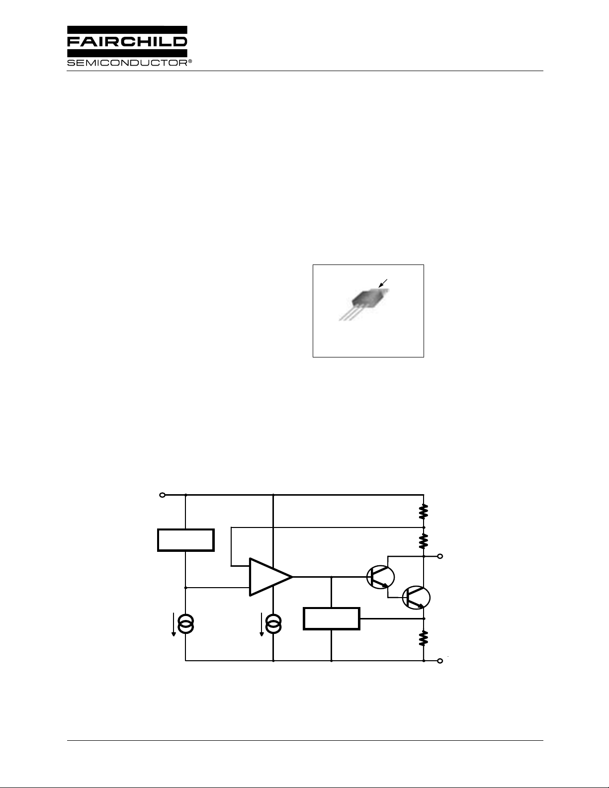
TO-220
1
1. GND 2. Input 3. Output
Vin
GND
VOLTAGE
REFERENCE
I1 I2
©2002 Fairchild Semiconductor Corporation
R1
R2
Out
Q2
Rsc
Output
In
Input
+
Q1
-
PROTECTION
CIRCUITRY
Rev. 1.0.1
Page 2
KA79XX/KA79XXA
Absolute Maximum Ratings
Parameter Symbol Value Unit
Input Voltage V
Thermal Resistance Junction-Case (Note1) R
Thermal Resistance Junction-Air (Note1, 2) R
Operating Temperature Range T
Storage Temperature Range T
Note:
1. Thermal resistance test board
Size: 76.2mm * 114.3mm * 1.6mm(1S0P)
JEDEC standard: JESD51 -3, JESD51-7
2. Assume no ambient airflow
I
θJC
θJA
OPR
STG
-35 V
5 °C/W
65 °C/W
0 ~ +125 °C
- 65 ~ +150 °C
Electrical Characteristics (KA7905)
(V
= -10V, IO = 500mA, 0°C ≤ T
I
Parameter Symbol Conditions Min. Typ. Max. Unit
Output Voltage V
Line Regulation (Note3) ∆V
Load Regulation (Note3) ∆V
Quiescent Current I
Quiescent Current Change ∆I
Temperature Coefficient of V
Output Noise Voltage V
Ripple Rejection RR f = 120Hz, ∆V
Dropout Voltage V
Short Circuit Current I
Peak Current I
≤ +125°C, C
J
O
O
O
Q
Q
∆Vo/∆TI
D
N
D
SC
PK
=2.2µF, CO =1µF, unless otherwise specified.)
I
TJ = +25°C -4.8 -5.0 -5.2
= 5mA to 1A, P
I
O
V
= -7V to -20V
I
TJ = +25°C
15W
O ≤
V
= -7V to -25V - 35 100
I
= -8V to -12V - 8 50
V
I
-4.75 -5.0 -5.25
TJ = +25°C, IO = 5mA to 1.5A - 10 100
=+25°C, IO = 250mA to 750mA - 3 50
T
J
TJ =+25°C-36mA
IO = 5mA to 1A - 0.05 0.5
= -8V to -25V - 0.1 0.8
V
I
= 5mA - -0.4 - mV/°C
O
f = 10Hz to 100kHz, TA = +25°C-40-µV
= 10V 54 60 - dB
I
TJ =+25°C, IO = 1A - 2 - V
TJ =+25°C, VI = -35V - 300 - mA
TJ =+25°C-2.2-A
V
mV
mV
mA
Note
3. Load and line regulation are specified at constant junction temperature. Changes in V
into account separately. Pulse testing with low duty is used.
2
due to heating e ffe cts mus t be t ak en
O
Page 3

KA79XX/KA79XXA
Electrical Characteristics (KA7906)
(V
= -11V, IO = 500mA, 0°C ≤ T
I
≤ +125°C, C
J
I
(Continued)
=2.2µF, CO = 1µF, unless otherwise specified.)
Parameter Symbol Conditions Min. Typ. Max. Unit
TJ =+25°C -5.75 -6 -6.25
Output Voltage V
Line Regulation (Note1) ∆V
Load Regulation (Note1) ∆V
Quiescent Current I
Quiescent Current Change ∆I
Temperature Coefficient of V
D
Output Noise Voltage V
Ripple Rejection RR f = 120Hz, ∆V
Dropout Voltage V
Short Circuit Current I
Peak Current I
O
I
O
V
I
TJ = +25°C
O
TJ = +25°C, IO = 5mA to 1.5A - 10 120
O
T
J
Q
TJ = +25°C-36mA
IO = 5mA to 1A - 0.05 0.5
Q
V
I
∆Vo/∆TI
N
D
SC
PK
O
f = 10Hz to 100kHz, TA =+25°C - 130 - µV
TJ = +25°C, IO = 1A - 2 - V
TJ = +25°C, VI = -35V - 300 - mA
TJ = +25°C-2.2-A
= 5mA to 1A, P
= -9V to -21V
≤ 15W
O
V
= -8V to -25V - 10 120
I
= -9V to -13V - 5 60
V
I
-5.7 -6 -6.3
= +25°C, IO = 250mA to 750mA - 3 60
= -8V to -25V - 0.1 1.3
= 5mA - -0.5 - mV/°C
= 10V 54 60 - dB
I
V
mV
mV
mA
Note
1. Load and line regulation are specified at constant junction temperature. Changes in V
into account separately. Pulse testing with low duty is used.
due to heating eff e cts mus t be t aken
O
3
Page 4
KA79XX/KA79XXA
Electrical Characteristics (KA7908)
(V
= -14V, IO = 500mA, 0°C ≤ T
I
≤ +125°C, C
J
(Continued)
=2.2µF, CO =1µF, unless otherwise specified.)
I
Parameter Symbol Conditions Min. Typ. Max. Unit
TJ =+25°C -7.7-8-8.3
Output Voltage V
Line Regulation (Note1) ∆V
Load Regulation (Note1) ∆V
Quiescent Current I
Quiescent Current Change ∆I
Temperature Coefficient of V
D
Output Noise Voltage V
Ripple Rejection RR f = 120Hz, ∆V
Dropout Voltage V
Short Circuit Current I
Peak Current I
O
I
O
V
I
TJ = +25°C
O
TJ = +25°C, IO = 5mA to 1.5A - 12 160
O
T
J
Q
TJ = +25°C-36mA
IO = 5mA to 1A - 0.05 0.5
Q
V
I
∆Vo/∆TI
N
D
SC
PK
O
f = 10Hz to 100kHz, TA = +25°C - 175 - µV
TJ =+25°C, IO = 1A - 2 - V
TJ =+25°C, VI = -35V - 300 - mA
TJ = +25°C-2.2-A
= 5mA to 1A, P
= -10V to -23V
≤ 15W
O
V
= -10.5V to -25V - 10 160
I
= -11V to -17V - 5 80
V
I
-7.6 -8 -8.4
= +25°C, IO = 250mA to 750mA - 4 80
= -10.5V to -25V - 0.1 1
= 5mA - -0.6 - mV/°C
= 10V 54 60 - dB
I
V
mV
mV
mA
Note
1. Load and line regulation are specified at constant junction temperature. Changes in V
into account separately. Pulse testing with low duty is used.
due to heating e ffe cts mus t be t ak en
O
4
Page 5
KA79XX/KA79XXA
Electrical Characteristics (KA7909)
(V
= -15V, IO = 500mA, 0°C ≤ T
I
≤ +125°C, C
J
(Continued)
=2.2µF, CO =1µF, unless otherwise specified.)
I
Parameter Symbol Conditions Min. Typ. Max. Unit
TJ = +25°C -8.7 -9.0 -9.3
Output Voltage V
Line Regulation (Note1) ∆V
Load Regulation (Note1) ∆V
Quiescent Current I
Quiescent Current Change ∆I
Temperature Coefficient of V
D
Output Noise Voltage V
Ripple Rejection RR f = 120Hz, ∆V
Dropout Voltage V
Short Circuit Current I
Peak Current I
O
I
O
V
I
TJ =+25°C
O
TJ =+25°C, IO = 5mA to 1.5A - 12 180
O
T
J
TJ = +25°C-36mA
Q
IO = 5mA to 1A - 0.05 0.5
Q
V
I
∆Vo/∆TI
N
D
SC
PK
O
f = 10Hz to 100kHz, TA = +25°C - 175 - µV
TJ = +25°C, IO = 1A - 2 - V
TJ = +25°C, VI = -35V - 300 - mA
TJ = +25°C-2.2-A
= 5mA to 1A, P
= -1.5V to -23V
≤ 15W
O
V
= -11.5V to -26V - 10 180
I
= -12V to -18V - 5 90
V
I
-8.6 -9.0 -9.4
=+25°C, IO = 250mA to 750mA - 4 90
= -11.5V to -26V - 0.1 1
= 5mA - -0.6 - mV/°C
= 10V 54 60 - dB
I
V
mV
mV
mA
Note
1. Load and line regulation are specified at constant junction temperature. Changes in V
into account separately. Pulse testing with low duty is used.
due to heating eff e cts mus t be t aken
O
5
Page 6

KA79XX/KA79XXA
Electrical Characteri stics (KA7910)
(V
= -17V, IO = 500mA, 0°C ≤T
I
≤ +125°C, C
J
I
(Continued)
=2.2µF, CO =1µF, unless otherwise specified.)
Parameter Symbol Conditions Min. Typ. Max. Unit
TJ = +25°C -9.6 -10 -10.4
Output Voltage V
Line Regulation (Note1) ∆V
Load Regulation (Note1) ∆V
Quiescent Current I
Quiescent Current Change ∆I
Temperature Coefficient of V
O
Output Noise Voltage V
Ripple Rejection RR f = 120Hz, ∆V
Dropout Voltage V
Short Circuit Current I
Peak Current I
O
I
O
V
I
TJ = +25°C
O
TJ = +25°C, IO = 5mA to 1.5A - 12 200
O
T
J
Q
TJ = +25°C-36mA
IO = 5mA to 1A - 0.05 0.5
Q
V
I
∆Vo/∆TI
N
D
SC
PK
O
10Hz ≤ f ≤ 100kHz, TA = +25°C - 280 - µV
TJ = +25°C, IO = 1A - 2 - V
TJ = +25°C, VI = -35V - 300 - mA
TJ = +25°C-2.2-A
= 5mA to 1A, P
= -12V to -28
≤ 15W
O
V
= -12.5V to -28V - 12 200
I
= -14V to -20V - 6 100
V
I
-9.5 -10 -10.5
= +25°C, IO = 250mA to 750mA - 4 100
= -12.5 to -28V - 0.1 1
= 5mA - -1 - mV/°C
= 10V 54 60 - dB
I
V
mV
mV
mA
Note
1. Load and line regulation are specified at constant junction temperature. Changes in V
into account separately. Pulse testing with low duty is used.
due to heating e ffe cts mus t be t ak en
O
6
Page 7

KA79XX/KA79XXA
Electrical Characteristics (KA7912)
(V
= -19V, IO = 500mA, 0°C ≤T
I
≤ +125°C, C
J
I
(Continued)
=2.2µF, CO =1µF, unless otherwise specified.)
Parameter Symbol Conditions Min. Typ. Max. Unit
TJ = +25°C -11.5 -12 -12.5
Output Voltage V
Line Regulation (Note1) ∆V
Load Regulation (Note1) ∆V
Quiescent Current I
Quiescent Current Change ∆I
Temperature Coefficient of V
D
Output Noise Voltage V
Ripple Rejection RR f = 120Hz, ∆V
Dropout Voltage V
Short Circuit Current I
Peak Current I
O
I
O
V
I
TJ = +25°C
O
TJ = +25°C, IO = 5mA to 1.5A - 12 240
O
T
J
TJ =+25°C-36mA
Q
IO = 5mA to 1A - 0.05 0.5
Q
V
I
∆Vo/∆TI
N
D
SC
PK
O
f = 10Hz to 100kHz, TA =+25°C - 200 - µV
TJ = +25°C, IO = 1A - 2 - V
TJ = +25°C, VI = -35V - 300 - mA
TJ = +25°C-2.2-A
= 5mA to 1A, P
= -15.5V to -27V
≤ 15W
O
V
= -14.5V to -30V - 12 240
I
= -16V to -22V - 6 120
V
I
-11.4 -12 -12.6
=+25°C, IO = 250mA to 750mA - 4 120
= -14.5V to -30V - 0.1 1
= 5mA - -0.8 - mV/°C
= 10V 54 60 - dB
I
V
mV
mV
mA
Note
1. Load and line regulation are specified at constant junction temperature. Changes in V
into account separately. Pulse testing with low duty is used.
due to heating eff e cts mus t be t aken
O
7
Page 8

KA79XX/KA79XXA
Electrical Characteristics (KA7915)
(V
= -23V, IO = 500mA, 0°C ≤T
I
≤ +125°C, C
J
I
(Continued)
=2.2µF, CO =1µF, unless otherwise specified.)
Parameter Symbol Conditions Min. Typ. Max. Unit
TJ = +25°C -14.4 -15 -15.6
Output Voltage V
Line Regulation (Note1) ∆V
Load Regulation (Note1) ∆V
Quiescent Current I
Quiescent Current Change ∆I
Temperature Coefficient of V
D
Output Noise Voltage V
Ripple Rejection RR f = 120Hz, ∆V
Dropout Voltage V
Short Circuit Current I
Peak Current I
O
I
O
V
I
TJ = +25°C
O
TJ = +25°C, IO = 5mA to 1.5A - 12 300
O
T
J
Q
TJ =+25°C-36mA
IO = 5mA to 1A - 0.05 0.5
Q
V
I
∆Vo/∆TI
N
D
SC
PK
O
f = 10Hz to 100kHz, TA = +25°C - 250 - µV
TJ = +25°C, IO = 1A - 2 - V
TJ = +25°C, VI = -35V - 300 - mA
TJ = +25°C-2.2-A
= 5mA to 1A, P
= -18V to -30V
≤ 15W
O
V
= -17.5V to -30V - 12 300
I
= -20V to -26V - 6 150
V
I
-14.25 -15 -15.75
=+25°C, IO = 250mA to 750mA - 4 150
= -17.5V to -30V - 0.1 1
= 5mA - -0.9 - mV/°C
= 10V 54 60 - dB
I
V
mV
mV
mA
Note
1. Load and line regulation are specified at constant junction temperature. Changes in V
into account separately. Pulse testing with low duty is used.
due to heating e ffe cts mus t be t ak en
O
8
Page 9

KA79XX/KA79XXA
Electrical Characteristics (KA7918)
(V
= -27V, IO = 500mA, 0°C ≤ T
I
≤ +125°C, C
J
(Continued)
=2.2µF, CO =1µF, unless otherwise specified.)
I
Parameter Symbol Conditions Min. Typ. Max. Unit
TJ = +25°C -17.3 -18 -18.7
Output Voltage V
Line Regulation (Note1) ∆V
Load Regulation (Note1) ∆V
Quiescent Current I
Quiescent Current Change ∆I
Temperature Coefficient of V
D
Output Noise Voltage V
Ripple Rejection RR f = 120Hz, ∆V
Dropout Voltage V
Short Circuit Current I
Peak Current I
O
I
O
V
I
TJ = +25°C
O
TJ = +25°C, IO = 5mA to 1.5A - 15 360
O
T
J
Q
TJ = +25°C-36mA
IO = 5mA to 1A - 0.05 0.5
Q
V
I
∆Vo/∆TI
N
D
SC
PK
O
f = 10Hz to 100kHz, TA = +25°C - 300 - µV
TJ = +25°C, IO = 1A - 2 - V
TJ = +25°C, VI = -35V - 300 - mA
TJ =+25°C-2.2-A
= 5mA to 1A, P
= -22.5V to -33V
≤ 15W
O
V
= -21V to -33V - 15 360
I
= -24V to -30V - 8 180
V
I
-17.1 -18 -18.9
= +25°C, IO = 250mA to 750mA - 5 180
= -21V to -33V - 0.1 1
= 5mA - -1 - mV/°C
= 10V 54 60 - dB
I
V
mV
mV
mA
Note
1. Load and line regulation are specified at constant junction temperature. Changes in V
into account separately. Pulse testing with low duty is used.
due to heating eff e cts mus t be t aken
O
9
Page 10

KA79XX/KA79XXA
Electrical Characteristics (KA7924)
(V
= -33V, IO = 500mA, 0°C ≤T
I
≤ +125°C, C
J
I
(Continued)
=2.2µF, CO =1µF, unless otherwise specified.)
Parameter Symbol Conditions Min. Typ. Max. Unit
TJ = +25°C -23 -24 -25
Output Voltage V
Line Regulation (Note1) ∆V
Load Regulation (Note1) ∆V
Quiescent Current I
Quiescent Current Change ∆I
Temperature Coefficient of V
Output Noise Voltage V
Ripple Rejection RR f = 120Hz, ∆V
Dropout Voltage V
Short Circuit Current I
Peak Current I
O
O
O
Q
Q
∆Vo/∆TI
D
N
D
SC
PK
= 5mA to 1A, P
I
O
= -27V to -38V
V
I
TJ =+25°C
≤ 15W
O
V
= -27V to -38V - 15 480
I
= -30V to -36V - 8 180
V
I
-22.8 -24 -25.2
TJ = +25°C, IO = 5mA to 1.5A - 15 480
= +25°C, IO = 250mA to 750mA - 5 240
T
J
TJ = +25°C-36mA
IO = 5mA to 1A - 0.05 0.5
= -27V to -38V - 0.1 1
V
I
= 5mA - -1 - mV/°C
O
f = 10Hz to 100kHz, TA =+25°C - 400 - µV
= 10V 54 60 - dB
I
TJ =+25°C, IO = 1A - 2 - V
TJ =+25°C, VI = -35V - 300 - mA
TJ =+25°C-2.2-A
V
mV
mV
mA
Note
1. Load and line regulation are specified at constant junction temperature. Changes in V
into account separately. Pulse testing with low duty is used.
due to heating e ffe cts mus t be t ak en
O
10
Page 11

KA79XX/KA79XXA
Electrical Characte ri sti cs (KA7905A)
(V
= -10V, IO = 500mA, 0°C ≤T
I
≤ +125°C, C
J
=2.2µF, CO =1µF, unless otherwise specified.)
I
(Continued)
Parameter Symbol Conditions Min. Typ. Max. Unit
TJ = +25°C -4.9 -5.0 -5.1
Output Voltage V
Line Regulation (Note1) ∆V
Load Regulation (Note1) ∆V
Quiescent Current I
Quiescent Current Change ∆I
Temperature Coefficient of V
D
Output Noise Voltage V
Ripple Rejection RR f = 120Hz, ∆V
Dropout Voltage V
Short Circuit Current I
Peak Current I
O
= 5mA to 1A, P
I
O
= -7V to -20V
V
I
TJ = +25°C
O
= -7.5V to -25V - 7 50
V
I
V
I
IO = 5mA to 1.5A
T
O
Q
J
T
J
TJ =+25°C-36mA
IO = 5mA to 1A - 0.05 0.5
Q
∆Vo/∆TI
N
D
SC
PK
= -8V to -25V - 0.1 0.8
V
I
= 5mA - -0.4 - mV/°C
O
f = 10Hz to 100kHz, TA =+25°C-40-µV
TJ = +25°C, IO = 1A - 2 - V
TJ = +25°C, VI = -35V - 300 - mA
TJ = +25°C-2.2-A
≤ 15W
O
VI = -7V to -20V
I
= 1A
O
= -8V to -12V
V
I
I
= 1A
O
-4.8 -5.0 -5.2
-550
-225
= -8V to -12V, IO=1A - 7 50
= +25°C
- 10 100
=+25°C, IO = 250mA to 750mA - 3 50
= 10V 54 60 - dB
I
V
mV
mV
mA
Note
1. Load and line regulation are specified at constant junction temperature. Changes in V
into account separately. Pulse testing with low duty is used.
due to heating eff e cts mus t be t aken
O
11
Page 12

KA79XX/KA79XXA
Electrical Characte ri sti cs (KA7912A)
(V
= -19V, IO = 500mA, 0°C ≤T
I
≤ +125°C, C
J
=2.2µF, CO =1µF, unless otherwise specified.)
I
(Continued)
Parameter Symbol Conditions Min. Typ. Max. Unit
TJ =+25°C -11.75 -12 -12.25
Output Voltage V
Line Regulation (Note1) ∆V
Load Regulation (Note1) ∆V
Quiescent Current I
Quiescent Current Change ∆I
Temperature Coefficient of V
D
Output Noise Voltage V
Ripple Rejection RR f = 120Hz, ∆V
Dropout Voltage V
Short Circuit Current I
Peak Current I
O
I
O
V
I
TJ = +25°C
O
V
I
V
I
TJ =+25°C, IO = 5mA to 1.5A - 12 150
O
T
J
Q
TJ =+25°C-36mA
IO = 5mA to 1A - 0.05 0.5
Q
V
I
∆Vo/∆TI
N
D
SC
PK
O
f = 10Hz to 100kHz, TA =+25°C - 200 - µV
TJ =+25°C, IO = 1A - 2 - V
TJ =+25°C, VI = -35V - 300 - mA
TJ =+25°C-2.2-A
= 5mA to 1A, P
= -15.5V to -27V
≤ 15W
O
VI = -14.5V to -27V
Io = 1A
= -16V to -22V
V
I
Io = 1A
-11.5 -12 -12.5
- 12 120
-660
= -14.8V to -30V - 12 120
= -16V to -22V, Io = 1A - 12 120
=+25°C, IO = 250mA to 750mA - 4 75
= -15V to -30V - 0.1 1
= 5mA - -0.8 - mV/°C
= 10V 54 60 - dB
I
V
mV
mV
mA
Note
1. Load and line regulation are specified at constant junction temperature. Changes in V
into account separately. Pulse testing with low duty is used.
due to heating e ffe cts mus t be t ak en
O
12
Page 13

KA79XX/KA79XXA
Electrical Characte ri sti cs (KA7915A)
(V
= -23V, IO = 500mA, 0°C ≤T
I
≤ +125°C, C
J
=2.2µF, CO =1µF, unless otherwise specified.)
I
(Continued)
Parameter Symbol Conditions Min. Typ. Max. Unit
TJ = +25°C -14.7 -15 -15.3
Output Voltage V
Line Regulation (Note1) ∆V
Load Regulation (Note1) ∆V
Quiescent Current I
Quiescent Current Change ∆I
Temperature Coefficient of V
D
Output Noise Voltage V
Ripple Rejection RR f = 120Hz, ∆V
Dropout Voltage V
Short Circuit Current I
Peak Current I
O
I
O
V
I
TJ =+25°C
O
V
I
V
I
TJ = +25°C, IO = 5mA to 1.5A - 12 150
O
T
J
TJ =+25°C-36mA
Q
IO = 5mA to 1A - 0.05 0.5
Q
V
I
∆Vo/∆TI
N
D
SC
PK
O
f = 10Hz to 100kHz, TA =+25°C - 250 - µV
TJ = +25°C, IO = 1A - 2 - V
TJ =+25°C, VI = -35V - 300 - mA
TJ =+25°C-2.2-A
= 5mA to 1A, P
= -18V to -30V
≤ 15W
O
VI = -17.5V to -30V
Io = 1A
= -20V to -26V
V
I
Io = 1A
-14.4 -15 -15.6
- 12 150
-675
= -17.9V to -30V - 12 150
= -20V to -26V, Io = 1A - 6 150
= +25°C, IO = 250mA to 750mA - 4 75
= -18.5V to -30V - 0.1 1
= 5mA - -0.9 - mV/°C
= 10V 54 60 - dB
I
V
mV
mV
mA
Note
1. Load and line regulation are specified at constant junction temperature. Changes in V
into account separately. Pulse testing with low duty is used.
due to heating eff e cts mus t be t aken
O
13
Page 14

KA79XX/KA79XXA
]
DtVlt[V]
A
Typical Performance Characteristics
5.1
5.05
Ou
tp
5
ut
Vo
4.95
lta
ge
4.9
[-
V
Output Voltage[-V]
4.85
4.8
-40 -25 0 25 50 75 100 125
Vin=10V
Io=40mA
TA, Ambient Temperature [oC]
Figure 1. Output Voltage
5
4.5
4
3.5
3
2.5
2
1.5
1
Quiescent Current [mA]
0.5
0
-40 -25 0 2 5 50 7 5 100 125
TA, Ambient Temperature [oC]
Vin=25V
Io=100mA
15
13
Lo
11
ad
9
Re
gul
7
ati
5
on
3
[m
1
V]
-1
-3
-5
Load Regulation[mV]
-40 -25 0 25 50 75 100 125
Io=1.5A
Io=0.75A
T
, Ambient Temperature [oC]
A
Figure 2. Load Regulation
4
3.5
3
2.5
2
1.5
1
Dropout Voltage [V]
0.5
0
-40-250 255075100125
Io=1A
TA, Ambient Temperature [oC]
Figure 3. Quiescent Current
0.6
0.55
Sh
0.5
ort
0.45
0.4
Cir
0.35
cui
0.3
t
0.25
Cu
0.2
rre
0.15
0.1
nt
0.05
[A]
Short Circuit Current[A]
0
-0.05
-0.1
-40 -25 0 25 50 75 100 125
, Ambient Temperature [oC]
T
Figure 4. Dropout Voltage
Figure 5. Short Circuit Current
14
Page 15

Typical Applications
KA79XX/KA79XXA
+15V
-15V
2.2uF
+
C
I
Input
Figure 6. Negative Fixed ou tput regulator
1
1
KA79XX
KA7812
C1
C1
+
+
0.33uF
2.2uF
2
2
1
KA7912
1uF
+
Co
32
Output
3
+
Co
1uF
1uF
+
Co
3
*
*
+12V
1N4001
GND
1N4001
-12V
Figure 7. Split power supply ( ±±±± 12V/1A)
Note:
(1) To specify an output voltage, substitute voltage value for "XX "
(2) Required for stability. For va lue giv en, capacitor must be sol i d ta nta lum . If aluminium electroni cs are used, at least ten times
value shown should be selected. C
(3) To improve transient response. If large capacitors are used, a high current diode from input to output (1N400l or similar)
should be introduced to protect the device from momentary input short circuit.
is required if regulator is located an appreciable distance from power supply filter.
I
15
Page 16

KA79XX/KA79XXA
Mechanical Dimensions
Package
Dimensions in millimeters
(1.70)
±0.20
9.20
±0.20
13.08
±0.10
1.30
(1.46)
(1.00)
1.27
±0.10
9.90
(8.70)
ø3.60
±0.20
±0.10
TO-220
(45°)
1.52
±0.10
(3.70)(3.00)
±0.10
2.80
±0.20
18.95MAX.
15.90
±0.30
10.08
4.50
±0.20
+0.10
1.30
–0.05
16
2.54TYP
[2.54
±0.20
]
10.00
±0.20
0.80
±0.10
2.54TYP
[2.54
±0.20
+0.10
0.50
–0.05
2.40
±0.20
]
Page 17

Ordering Information
Product Number Output Voltage Tolerance Package Operating Temperature
KA7905
KA7906
KA7908
KA7909
±
KA7910
KA7912
KA7915
KA7918
KA7924
KA7905A
KA7915A
4%
TO-220 0 ~ +125°C
±
2%KA7912A
KA79XX/KA79XXA
17
Page 18

KA79XX/KA79XXA
DISCLAIMER
FAIRCHILD SEMICONDUCTOR RESERVES THE RIGHT TO MAKE CHANGES WITHOUT FURT HER NOTICE TO ANY
PRODUCTS HEREI N TO IMPROVE RELIABILITY, FUNCTIO N OR DESIGN. FAIRCH IL D DOES NOT ASSUME ANY
LIABILITY ARISING OUT OF THE APPLICATION OR USE OF ANY PRODUCT OR CIRCUIT DESCRIBED HEREIN; NEITHER
DOES IT CONVEY ANY LICENSE UNDER IT S PATENT RIGHTS, NOR THE RIGHTS OF OTHE RS.
LIFE SUPPORT POL I CY
FAIRCHILD’S PR ODUCTS ARE NOT AUTH ORIZED FOR USE AS C RITICAL COMPONENT S IN LIFE SUPPORT DE VICES
OR SYSTEMS WITHOUT THE EXPRESS WRITTEN APPROVAL OF THE PRESIDENT OF FAIRCHILD SEMICONDUCTOR
CORPORATION. As used herein :
1. Life support devices or systems are devices or systems
which, (a) are intended for surgical implant into the body,
or (b) support or sustain life, and (c) whose failure to
perform when properly used in accordance with
2. A critical component in any component of a life support
device or sy stem whose fai lure to perform can be
reasonably expec ted to cause the failur e of the life support
device or system, or to affect its safety or effec t iv ene ss .
instructions for use provided in the labeling, can be
reasonably expected to result in a significant injury of the
user.
www.fairchildsemi.com
11/12/02 0.0m 001
2002 Fairchild Semiconductor Corporation
Stock#DSxxxxxxxx
 Loading...