

Page 1
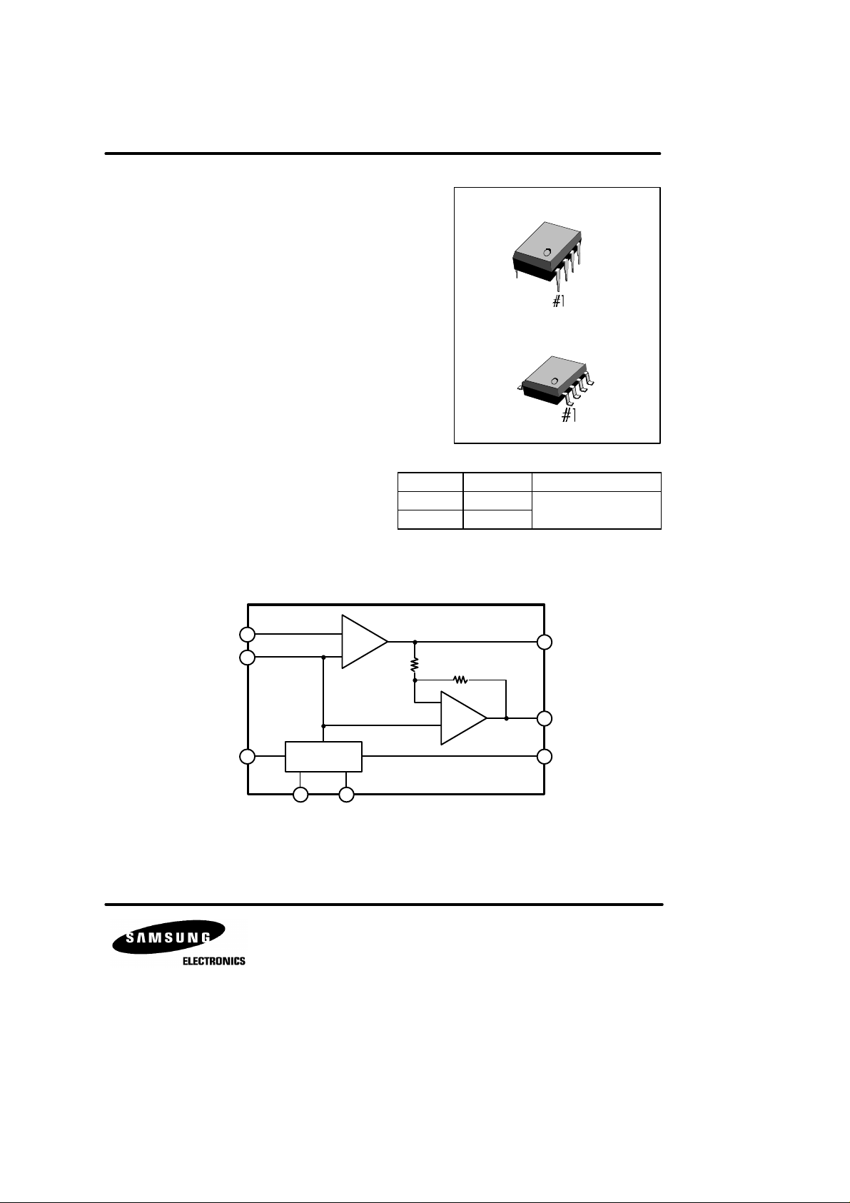
KA8602B LOW VOLTAGE AUDIO AMPLIFIER
ORDERING INFORMATION
INTRODUCTION
The KA8602B is the audio power amplifier available for
low voltages. KA8602B supplies differential outputs for maximizing output swing at low voltages. KA8602B doesn't
need coupling capacitors to the speaker. The gain of
this amp is controlled easily by two external resistors.
FEATURES
l Wide Supply Voltage (2 ~ 16V)
l Low Quiescent Supply Current (I
l Easy Gain Control
l Medium Output Power
= 2.7mA : Typ)
CC
PO = 250mW at VCC = 6V, RL = 32Ω, THD = 10%
l Minimum External Parts
l Load Impedance Range (8Ω~ 100Ω)
l Low Distortion
l Mute Function (l
= 65µA : Typ)
CC
BLOCK DIAGRAM
8-DIP-300
8-SOP-225
Device Package Operating Temperature
KA8602B 8-DIP-300
KA8602BD 8-SOP-225
- 20°C ~ + 70°C
INPUT(-)
2
INPUT(+)
1
4 BIAS CIRCUIT
Vcc
8 5
RIPPLE
REJECTION
GND
-
Amp1
+
Fig. 1
OUTPUT1
3
R
R
-
Amp2
6
OUTPUT2
+
MUTE
7
Page 2
KA8602B LOW VOLTAGE AUDIO AMPLIFIER
l l l
l
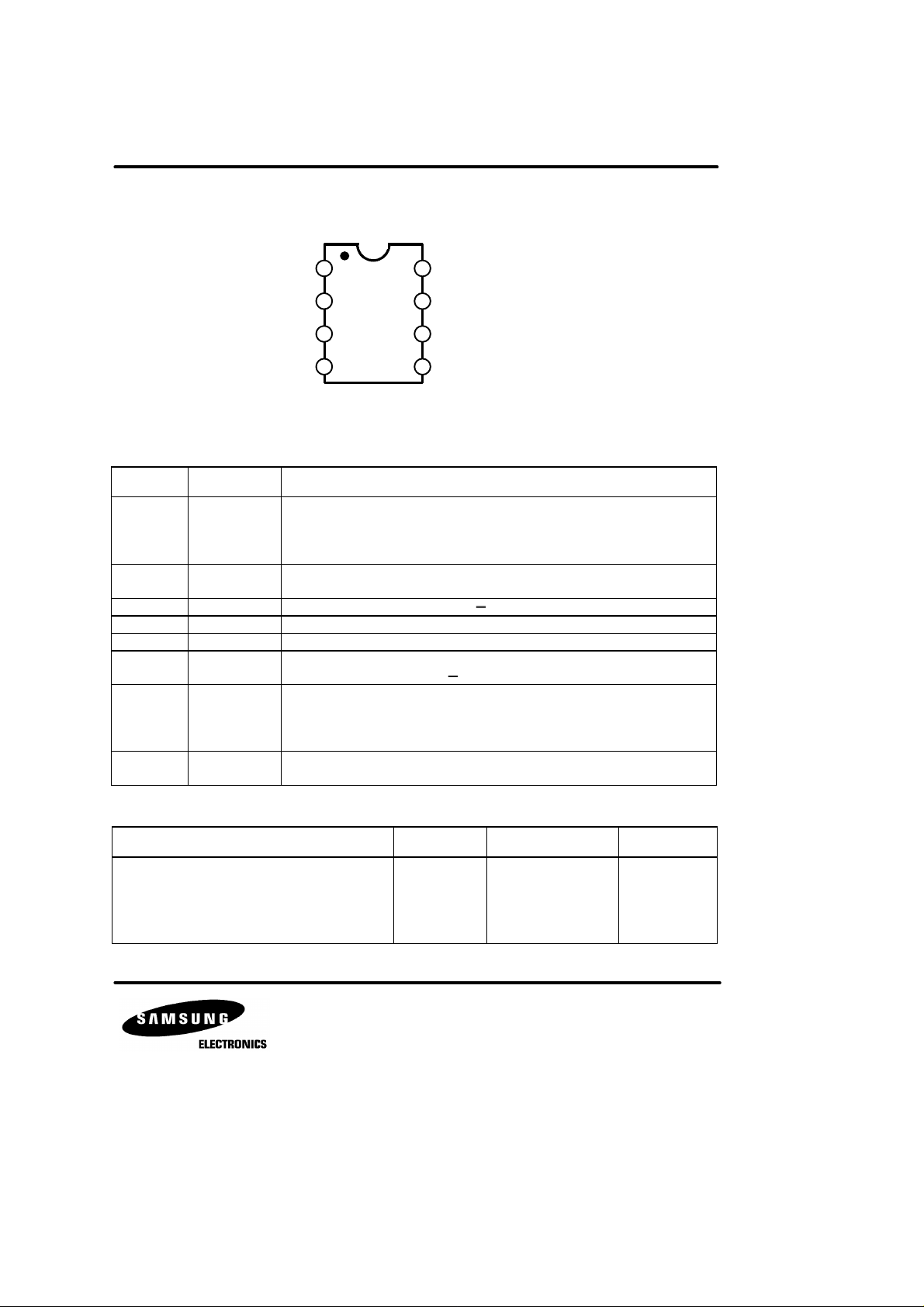
PIN CONFIGURATION
INPUT(+)
INPUT(-)
1
2
8
RIPPLE REJECTION
7
MUTE
KA8602B
OUTPUT1
Vcc
3
4
6
5
OUTPUT2
GND
Fig. 2
PIN DESCRIPTION
Pin No Symbol Description
Analog Ground for the amplifiers. A 1.0µF capacitor at this pin (with a 5.0µF
1 Input (+)
2
Input (-)
3 Output 1 Amplifier 1’s output. The DC Level is (VCC - 0.7V)/2.
4 V
CC
5 GND Ground pin.
6 Output 2
7 Mute
8
Ripple
Rejection
capacitor at pin 8) provides 52dB (Typ) of power supply rejection. Turn-on time of
the circuit is affected by the capacitor on this pin. This pin can be used as an
alternative input.
Amplifier input. The input capacitor and resistor set low frequency roll-off and input
impedance. The feedback resistor is connected between this pin and output1.
DC supply voltage (+2.0 ~ + 16V) is applied to this pin.
Amplifier 2’s output. This signal is equal in amplitude, but 180o out of phase with
that at output1. The DC level is (VCC - 0.7V)/2.
This pin can be used to power down the IC to conserve power, or for muting, or
both. When at a logic “Low” (0 to 0.8 volts), the KA8602B is enabled for normal
operation. When at a logic “High” (2.0 to VCC volts), the IC is disabled. If Mute is
open, that is equivalent to a logic “Low”.
A capacitor at this pin increases power supply rejection, and affects turn-on time.
This pin can be left open if the capacitor at pin 1 is sufficient.
ABSOLUTE MAXIMUM RATINGS
Characteristic Symbol Vale Unit
Supply Voltage
Output Current (output pin)
Maximum Voltage (input, Ripple rejection, Mute pin)
Applied Output Voltage (output pin) when disabled
Junction Temperature
V
V
CC
I
O
I (MAX)
V
O
T
J
- 1.0 ~ + 18
± 250
- 1.0 ~ VCC + 1.0
- 1.0 ~ VCC + 1.0
- 55 ~ + 140
V
mA
V
V
°C
Page 3
KA8602B LOW VOLTAGE AUDIO AMPLIFIER
(RL = 0)
RECOMMENDED OPERATING CONDITIONS (Ta = 25°C)
Characteristic Symbol Min Typ Max Unit
Supply Voltage
Load Impedance
Peak Load Current
Differential Gain (5KHz Bandwidth)
Voltage at Mute (Pin 7)
Ambient Temperature
ELECTRICAL CHARACTERISTIC
(VCC = 6V, Ta = 25°C, unless otherwise noted)
Characteristic Symbol Test Conditions Min Typ Max Unit
DC ELECTRICAL CHARACTERISTICS
Operating Current
Output Voltage (output pin) V
Output Offset Voltage V
Output High Level V
Output Low Level V
Input Bias Current (pin 2) I
Equivalent Resistance R
Input Low Voltage V
Mute Input High Voltage V
Input Resistance R
AC ELECTRICAL CHARACTERISTICS
Open Loop Gain (Amp 1) G
Close Loop Gain (Amp 2) G
Output Power P
Total Harmonic Distortion
(f = 1.0KHz)
Gain Bandwidth Product GBW 1.5 MHz
Power Supply Rejection
(VCC = 6.0V, ∆VCC = 3.0V)
Muting G
I
CC
O
OO
OH
OL
BIAS
EQ
IL (MUTE)
IH (MUTE)
I (MUTE)
V (AMP1)
V (AMP2)
O
THD
PSRR
V (MUTE)
I
V
V
CC
Z
L
L (PK)
∆G
V
I (MUTE)
Ta
+2.0
8
0
0
-20
+16
100
± 200
V
470
VCC = 3.0V, Mute = 0.8V
VCC = 16.0V, Mute = 0.8V
VCC = 3.0V, Mute = 2.0V 65 100
RL = 16Ω
R1 = 75KΩ
VCC = 3.0V
VCC = 6.0V
VCC = 12.0V
VCC = 6.0V, Rf = 75KΩ, RL = 32Ω
2.0V ≤ V
2.0V ≤ V
CC
CC
≤ 16V, I
≤ 16V, I
= -75mA
out
= 75mA
out
pin 1
1.0 1.15
-30 0 +30 mV
1001815025220
pin 8
2.0 V
VCC = Mute = 16V 50 90 175
80 dB
f = 1.0KHz, RL = 32Ω
V
= 3.0V, RL = 6Ω, THD ≤ 10%
CC
V
= 6.0V, RL = 32Ω, THD ≤ 10%
CC
V
= 12V, RL = 100Ω, THD ≤ 10%
CC
V
= 6.0V, RL = 32Ω, PO =125mW
CC
-0.35 0 +0.35 dB
55
250
400
VCC≤3.0V, RL = 8Ω, PO = 20mW
VCC≤12V, RL = 32Ω, PO = 200mW
C1 = ∞, C2 = 0.01µF
C
=0.1µF, C2=0, f=1.0KHz
1
50
C1 = 1.0µF, C2 = 5.0µF, f = 1.0KHz
Mute = 2.0V, 1.0Khz ≤ f ≤ 20KHz
V
Ω
mA
46
CC
dB
V
°C
2.7
4.0
3.3
5.0
1.25
2.65
5.65
VCC-1.0 V
0.16 V
-100 -200 nA
40
0.8 V
mW
0.5
1.0
0.5
0.6
12
52
> 70 dB
mA
µA
V
KΩ
KΩ
%
dB
Page 4
KA8602B LOW VOLTAGE AUDIO AMPLIFIER
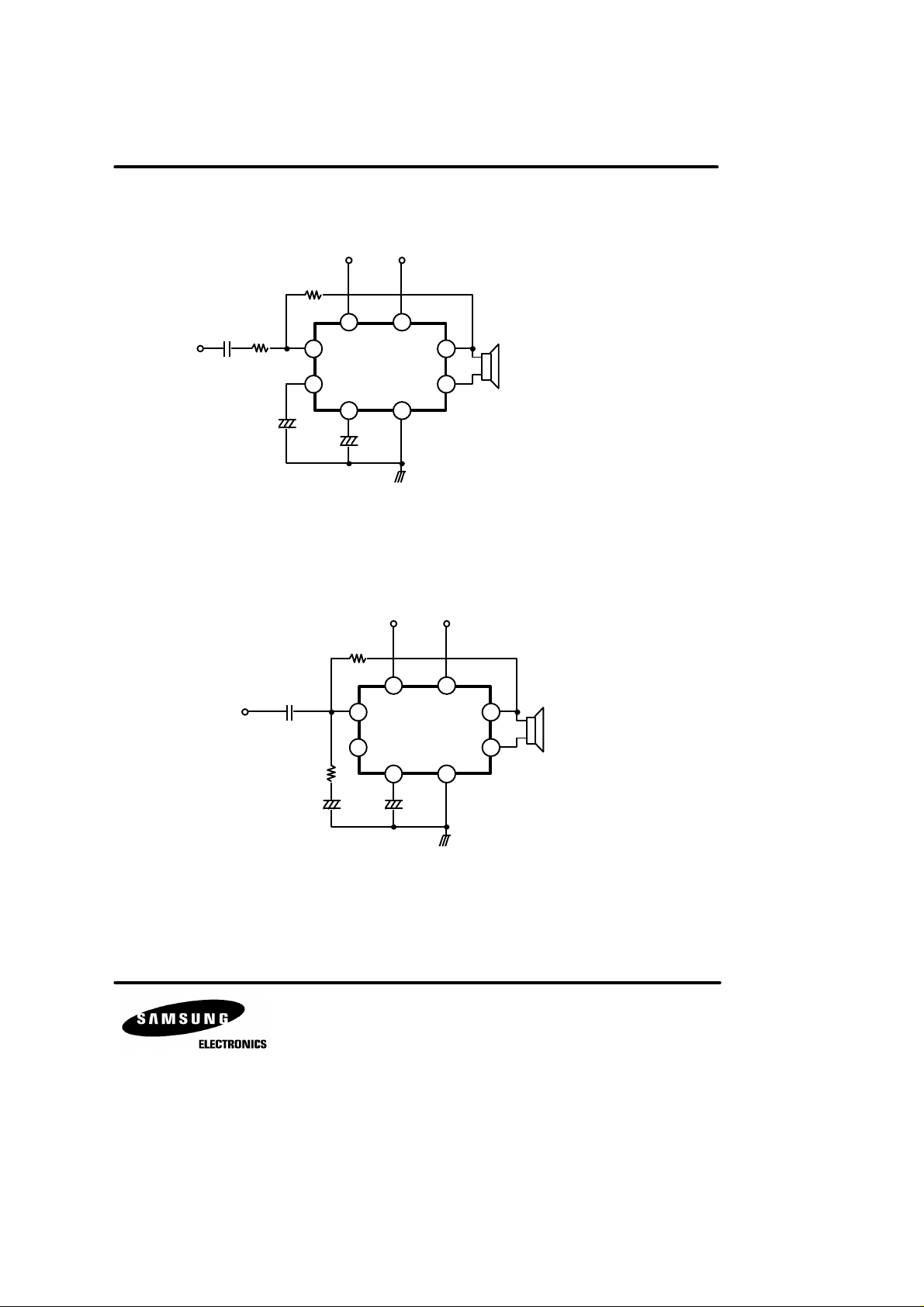
APPLICATION CIRCUIT
Vcc Mute
R
f
Audio
Input
0.1µF
R
i
+
1µF
2
1
4 7
KA8602B
8 5
+
5µF
Fig. 3
75K
Audio
Input
0.1µF
2
1
3K
+ +
0.1µF 5µF
3
6
Vcc Mute
4 7
KA8602B
8 5
Speaker
3
Speaker
6
Fig. 4
Page 5
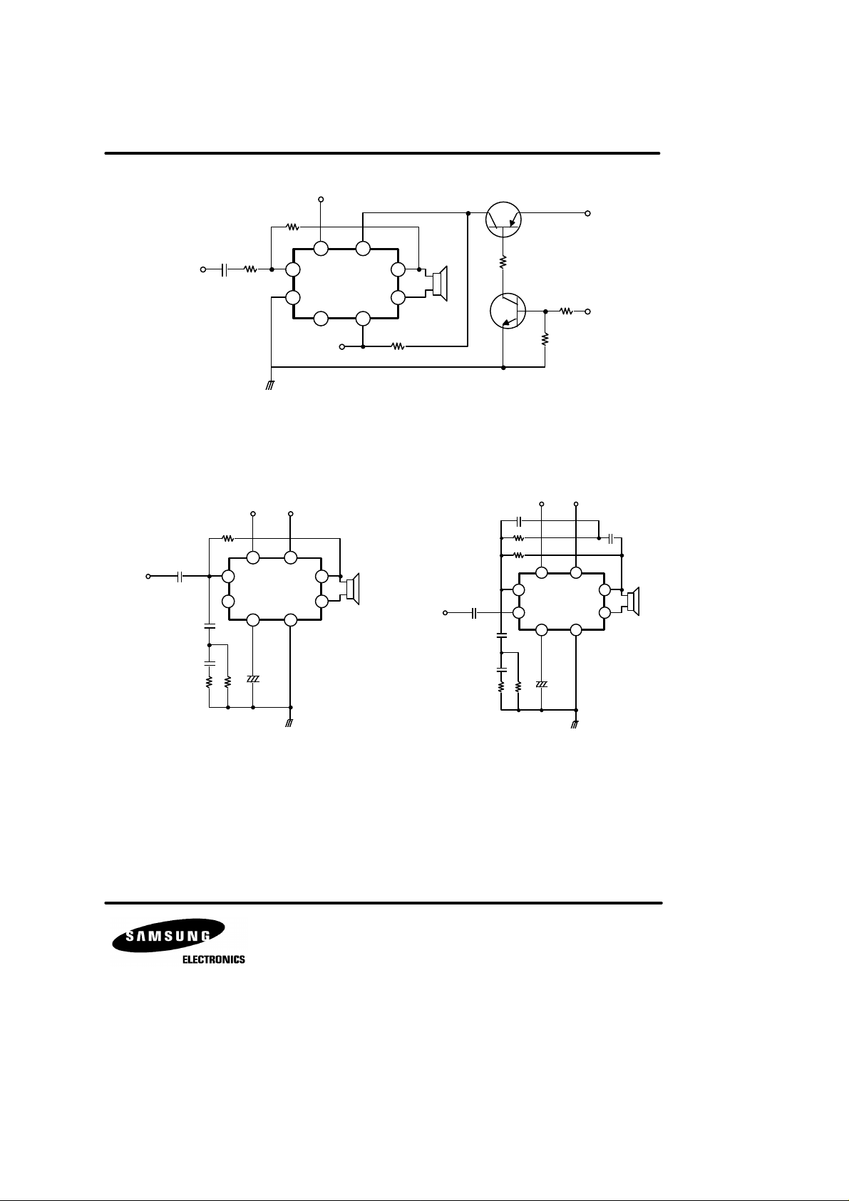
KA8602B LOW VOLTAGE AUDIO AMPLIFIER
Vcc(1.0 ~8.0V)
75K
4 7
0.1µF
Audio
Input
3K
2
KA8602B
1
8 5
VEE( -1.0 ~ -8.0V)
10K 20K
Fig. 5
Vcc Mute
75K
4 7
2
KA8602B
1
8 5
503
3
Speaker
6
Audio
Input
0.1µF
Vcc
3
6
Speaker
0.1µF
Audio
Input
4.7K
101
100K
100K
503
2
1
20K
Vcc Mute
4 7
KA8602B
8 5
Mute
100
3
Speaker
6
503
5.1K
5.1K
+
5µF
503
5.1K
5.1K
Fig. 6 Fig. 7
+
5µF
 Loading...