

Page 1
©2001 Fairchild Semiconductor Corporation
www.fairchildsemi.com
Rev. 1.0.1
Features
• Fixed Output Voltage of +3.3V
• Space Saving SMD types of DPAK
• 1V(Typ) Dropout at Io=800mA
• Output Current of 800mA
• Thermal Shutdown Protection
• Over Current Protection
• Output trimmed to +/-1% Tolerance
• No minimum Load Requ i re m en t
Description
The KA78RH33 i s a +3.3V fixed Low Dropout Voltage
Regulator specifically designed for use in low voltage operation. The maximum load current is 0.8A and the dropout
voltage is guaranteed to be 1V(Typ). The Dropout Voltage
varies with load current. The regulator consists of composite PNP-NPN pass transistors.
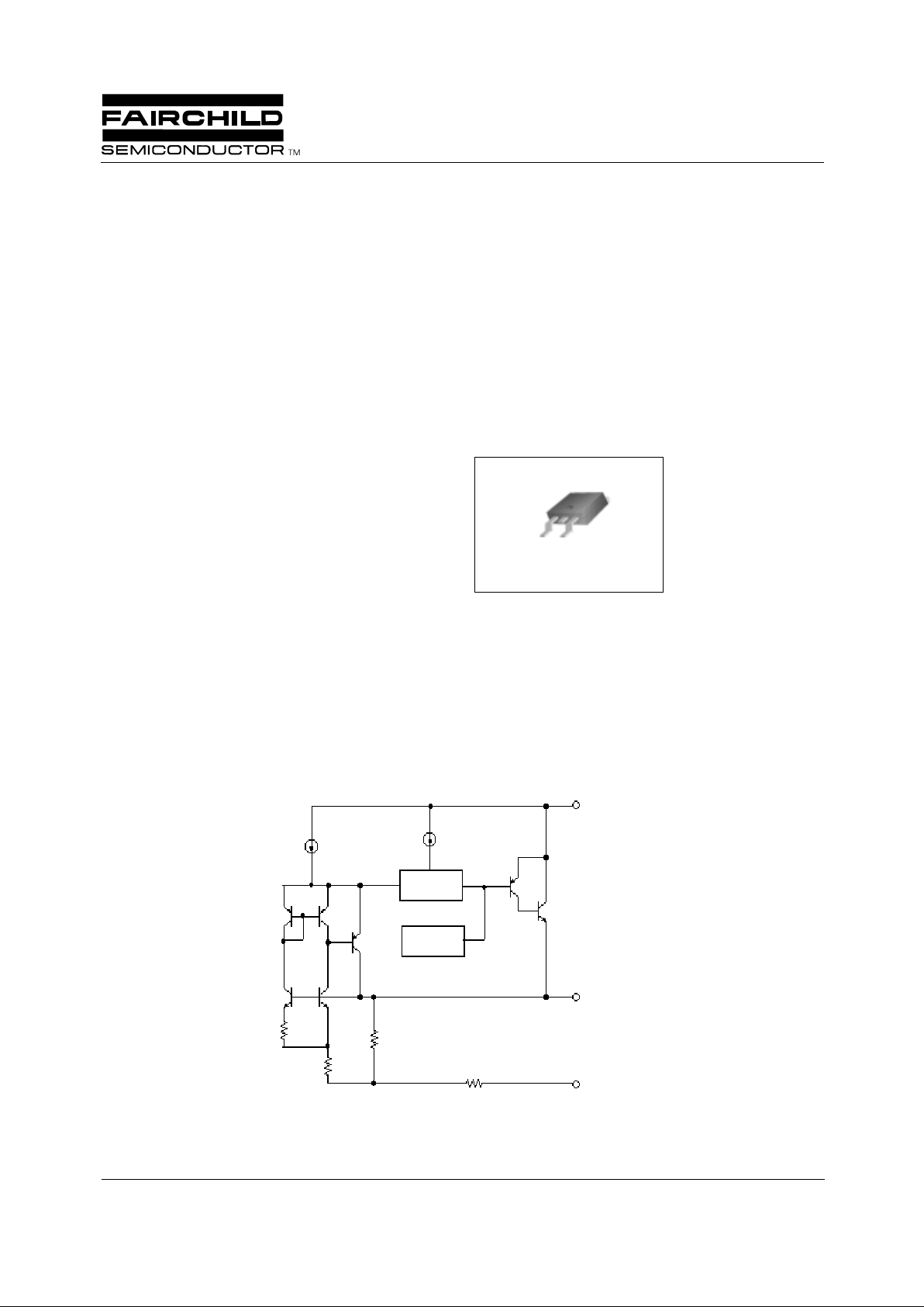
D-PAK
1. GND 2. Vout 3.Vin
1
Internal Block Diagram
3.Vin
2.Vout
1.GND
CURRENT
GENERATOR
PROTECTION
CIRCUIT
KA78RH33
Semi Low Dropout Voltage Regulator
Page 2
KA78RH33
2
Absolute Maximum Ratings
Temperature Characteristics
Electrical Characteristics
(Refer to the test circuit. Vin= 5V, Co=10uF, Ta = 25°C, unless otherwise specified.)
Parameter Symbol Value Unit
Power Supply Input Voltage Vin 15 V
Output Load Current Io 800 mA
Junction Temperature Tj 150 °C
Operating Junction Temperature Topr -25 ~ 125 °C
Storage Temperature Tstg -55 ~ 150 °C
Parameter Symbol Value Unit
Temperature Coefficient of Output Voltage △ Vo/ △ T + / -0.02 % / °C
Parameter Symbol Conditions Min. Typ. Max. Unit
Output Voltage Vout Io=10mA, Tj=25°C 3.27 3.3 3.33 V
Output Voltage Vout
Vin = 4.8V to 12V
Io = 10mA to 800mA
Tj = -25°C to 125°C
3.23 3.3 3.37 V
Line Regulation Rline Vin=4.8V to 12V, Io=10mA - 1 10 mV
Load Regulation Rload Io = 10mA to 800mA - 1 20 mV
Ripple Rejection RR
f=120Hz, Io=500mA
Vin = 6.3 +/- 1Vrms
55 - - dB
Dropout Voltage Vdrop
Io = 100mA
Io = 500mA
Io = 800mA
-
-
-
1
1.05
1.1
1.2
1.25
1.4
V
Quiescent Current Iq Vin <= 12V - 5 10 mA
Temperature Coefficient of
Output Voltage
△ Vo/ △ T
Tj = -25°C to 125°C
Io = 10mA
-0.2-mV/°C
Peak Output Current Ipk Vin = 6.3V 800 - - mA
Output Noise Voltage Vn f = 10Hz to 10KHz - 100 - µVrms
Page 3

KA78RH33
3
Typical Application
An input capacitor, Cin is not necessary for stability, but it will improve the overall performance
KA78RH33
Vin
Vout
Cin
0.1uF
Co
10uF
Gnd
Page 4

KA78RH33
4
Mechanical Dimensions
Package
Dimensions in millimeters
6.60 ±0.20
2.30 ±0.10
0.50 ±0.10
5.34 ±0.30
0.70 ±0.20
0.60 ±0.20
0.80 ±0.20
9.50 ±0.30
6.10 ±0.20
2.70 ±0.20
9.50 ±0.30
6.10 ±0.20
2.70 ±0.20
MIN0.55
0.76 ±0.10
0.50 ±0.10
1.02 ±0.20
2.30 ±0.20
6.60 ±0.20
0.76 ±0.10
(5.34)
(1.50)
(2XR0.25)
(5.04)
0.89 ±0.10
(0.10) (3.05)
(1.00)
(0.90)
(0.70)
0.91
±0.10
2.30TYP
[2.30±0.20]
2.30TYP
[2.30±0.20]
MAX0.96
(4.34)(0.50) (0.50)
D-PAK
Page 5

KA78RH33
5
Ordering Information
Product Number Package Operating Temperature
KA78RH33R D-PAK -25°C to + 125°C
Page 6

KA78RH33
2/20/01 0.0m 001
Stock#DSxxxxxxxx
2001 Fairchild Semiconductor Corporation
LIFE SUPPORT POL I CY
FAIRCHILD’S PRODUCTS ARE NOT AUTHORIZED FOR USE AS CRITICAL COMPONENTS IN LIFE SUPPORT DEVICES
OR SYSTEMS WITHOUT THE EXPRESS WRITTEN APPROVAL OF THE PRESIDENT OF FAIRCHILD SEMICONDUCTOR
CORPORATION. As used herein :
1. Life support devices or systems are devices or systems
which, (a) are intended for surgical implant into the body,
or (b) support or sustain life, and (c) whose failure to
perform when properly used in accordance with
instructions for use provided in the labeling, can be
reasonably expected to result in a significant injury of the
user.
2. A critical component in any component of a life support
device or sys tem whose failure to perform can be
reasonably expec ted to cause the failur e of the life support
device or system, or to affect its safety or effec tiveness.
www.fairchildsemi.com
DISCLAIMER
FAIRCHILD SEMICONDUCTOR RESERVES THE RIGHT TO MAKE CHANGES WITHOUT FURTHER NOTICE TO ANY
PRODUCTS HEREI N TO IMPROVE RELIABILITY, FUNCTION OR DES IGN. FAIRCHILD DOES NOT ASSUME ANY
LIABILITY ARISING OUT OF THE APPLICATION OR USE OF ANY PRODUCT OR CIRCUIT DESCRIBED HEREIN; NEITHER
DOES IT CONVEY ANY LICENSE UNDER ITS PATENT RIGHTS, NOR THE RI GHTS OF OTHERS.
 Loading...