

Page 1
J/SST270 Series
Vishay Siliconix
P-Channel JFETs
J270 SST270
J271 SST271
PRODUCT SUMMARY
Part Number V
J/SST270 0.5 to 2.0 30 6 –2
J/SST271 1.5 to 4.5 30 8 –6
FEATURES BENEFITS APPLICATIONS
D Low Cutoff Voltage: J270 <2 V
D High Input Impedance
D Very Low Noise
D High Gain
GS(off)
(V) V
(BR)GSS
Min (V) gfs Min (mS) I
Min (mA)
DSS
D Full Performance from Low-Voltage Power
Supply: Down to 2 V
D Low Signal Loss/System Error
D High System Sensitivity
D High-Quality, Low-Level Signal Amplification
D High-Gain, Low-Noise Amplifiers
D Low-Current, Low-Voltage Battery
Amplifiers
D Ultrahigh Input Impedance Pre-Amplifiers
D High-Side Switching
DESCRIPTION
The J/SST270 series consists of all-purpose amplifiers for
designs requiring p-channel operation.
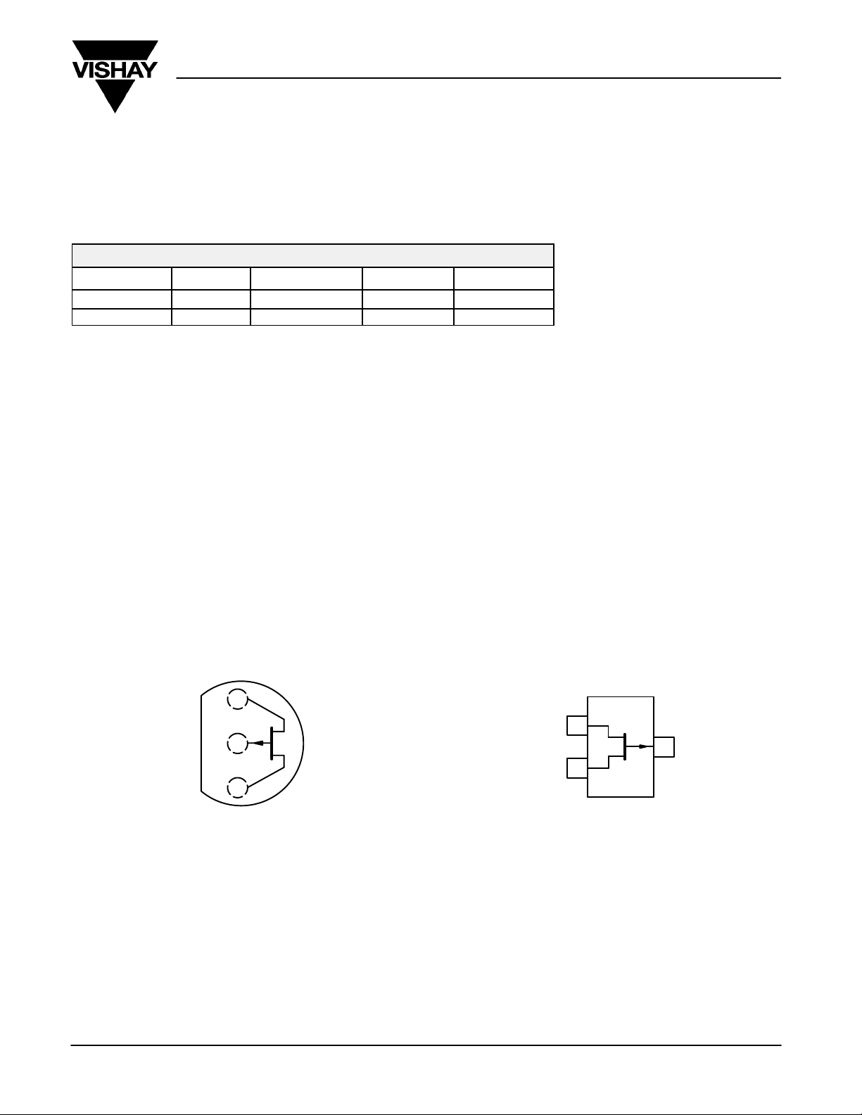
The TO-226AA (TO-92) plastic package provides a low-cost
option, while the TO-236 (SOT-23) package
TO-226AA
(TO-92)
D
G
S
1
2
3
Top View
J270
J271
provides surface-mount capability. Both the J and SST series
are available in tape-and-reel for automated assembly (see
Packaging Information).
TO-236
(SOT-23)
1
D
3
G
2
S
Top View
SST270 (S0)*
SST271 (S1)*
*Marking Code for TO-236
ABSOLUTE MAXIMUM RATINGS
Gate-Drain Voltage 30 V. . . . . . . . . . . . . . . . . . . . . . . . . . . . . . . . . . . . . . . . . . . . .
Gate-Source Voltage 30 V. . . . . . . . . . . . . . . . . . . . . . . . . . . . . . . . . . . . . . . . . . . .
Gate Current –50 mA. . . . . . . . . . . . . . . . . . . . . . . . . . . . . . . . . . . . . . . . . . . . . . . .
Storage Temperature –55 to 150_C. . . . . . . . . . . . . . . . . . . . . . . . . . . . . . . . . . .
Operating Junction Temperature –55 to 150_C. . . . . . . . . . . . . . . . . . . . . . . . . .
Document Number: 70258
S-04233—Rev. D, 02-Jul-01
Lead Temperature (
Power Dissipation
Notes
a. Derate 2.8 mW/_C above 25_C
1
/16” from case for 10 sec.) 300_C. . . . . . . . . . . . . . . . . . .
a
350 mW. . . . . . . . . . . . . . . . . . . . . . . . . . . . . . . . . . . . . . . . .
www.vishay.com
8-1
Page 2
J/SST270 Series
Vishay Siliconix
SPECIFICATIONS (TA = 25_C UNLESS OTHERWISE NOTED)
Parameter Symbol Test Conditions TypaMin Max Min Max Unit
Static
Limits
J/SST270 J/SST271
Gate-Source Breakdown Voltage V
Gate-Source Cutoff Voltage V
Saturation Drain Current
b
(BR)GSS
GS(off)
I
DSS
IG = 1 mA , VDS = 0 V
VDS = –15 V, ID = –1 nA 0.5 2.0 1.5 4.5
VDS = –15 V, VGS = 0 V –2 –15 –6 –50 mA
45 30 30
V
VGS = 20 V, VDS = 0 V 10 200 200 pA
Gate Reverse Current I
Gate Operating Current I
Drain Cutoff Current I
Gate-Source Forward Voltage V
GSS
G
D(off)
GS(F)
TA = 125_C
5 nA
VDG = –15 V, ID = –1 mA 10
VDS = –15 V, VGS = 10 V –10
IG = –1 mA , VDS = 0 V –0.7 V
pA
Dynamic
Common-Source Forward Transconductance g
Common-Source Output Conductance g
Common-Source Input Capacitance C
Common-Source
Reverse Transfer Capacitance
Equivalent Input Noise Voltage e
Notes
a. Typical values are for DESIGN AID ONLY, not guaranteed nor subject to production testing. PSCIA
b. Pulse test: PW v300 ms duty cycle v3%.
fs
os
iss
C
rss
n
VDS = –15 V, VGS = 0 V
VDS = –15 V, VGS = 0 V
f = 1 kHz
VDS = –15 V, VGS = 0 V
f = 1 MHz
VDG = –10 V, VGS = 0 V
f = 1 kHz
6 15 8 18 mS
200 500
20
4
20
mS
pF
nV⁄
√Hz
TYPICAL CHARACTERISTICS (TA = 25_C UNLESS OTHERWISE NOTED)
200
160
120
80
– Drain-Source On-Resistance ( Ω )
40
DS(on)
r
0
0681042
www.vishay.com
8-2
On-Resistance and Drain Current
vs. Gate-Source Cutoff Voltage
I
DSS
r
DS
rDS @ ID = –1 mA, VGS = 0 V
@ VDS = –15 V, VGS = 0 V
I
DSS
V
– Gate-Source Cutoff Voltage (V)
GS(off)
Forward Transconductance and Output Conductance
–100
I
DSS
–80
– Saturation Drain Current (mA)
–60
–40
–20
0
18
15
12
– Forward Transconductance (mS)
fs
g
vs. Gate-Source Cutoff Voltage
g
fs
g
os
9
6
gfs and gos @ VDS = –15 V
= 0 V, f = 1 kHz
V
GS
3
0
V
GS(off)
4
68102
– Gate-Source Cutoff Voltage (V)
250
200
150
100
50
0
g
os
– Output Conductance (µS)
Document Number: 70258
S-04233—Rev. D, 02-Jul-01
Page 3

TYPICAL CHARACTERISTICS (TA = 25_C UNLESS OTHERWISE NOTED)
Output Characteristics
VGS = 0 V
0.5 V
–1.6
–1.2
–2
Output Characteristics
VGS = 0 V
0.2 V
0.4 V
0.6 V
–2
–1.6
–1.2
J/SST270 Series
Vishay Siliconix
1.0 V
1.5 V
2.0 V
–0.8
– Drain Current (mA)
D
I
–0.4
0
0 –0.6 –0.8 –1
–25
V
GS(off)
–20
–15
–10
– Drain Current (mA)
D
I
–5
0
0 –12 –16 –20
–0.4–0.2
VDS – Drain-Source Voltage (V)
Output Characteristics
= 3 V
–8–4
VDS – Drain-Source Voltage (V)
Transfer Characteristics
–10
= 1.5 V
GS(off)
V
GS(off)
VDS = –15 VV
0.8 V
= 1.5 V
VGS = 0 V
0.5 V
1.0 V
1.5 V
2.0 V
–0.8
– Drain Current (mA)
D
I
–0.4
0
0 –0.3 –0.4 –0.5
30
24
18
12
Capacitance (pF)
6
0
01216820
–40
GS(off)
V
= 3 V
GS(off)
–0.2–0.1
VDS – Drain-Source Voltage (V)
Capacitance vs. Gate-Source Voltage
VDS = 0 V
f = 1 MHz
C
iss
C
rss
4
VGS – Gate-Source Voltage (V)
Transfer Characteristics
= 3 V
VDS = –15 VV
–8
–6
–4
– Drain Current (mA)
D
I
–2
0
0 0.2 0.4 0.6 0.8 1.0
Document Number: 70258
S-04233—Rev. D, 02-Jul-01
125_C
TA = –55_C
25_C
V
– Gate-Source Voltage (V)
GS
–32
–24
–16
– Drain Current (mA)
D
I
–8
TA = –55_C
125_C
0
012345
25_C
VGS – Gate-Source Voltage (V)
www.vishay.com
8-3
Page 4

J/SST270 Series
Vishay Siliconix
TYPICAL CHARACTERISTICS (TA = 25_C UNLESS OTHERWISE NOTED)
100
Transconductance vs. Drain Current Output Conductance vs. Drain Current
V
= 3 V
GS(off)
10
– Forward Transconductance (mS)
fs
g
1
–0.1 –1 –10
250
TA = 25_C
200
V
GS(off)
150
100
– Drain-Source On-Resistance ( Ω )
50
DS(on)
r
0
–1 –10 –100
100
25_C
– Drain Current (mA) ID – Drain Current (mA)
I
D
On-Resistance vs. Drain Current
= 1.5 V
3 V
ID – Drain Current (mA)
Noise Voltage vs. Frequency
VDS = –15 V
f = kHz
TA = –55_C
125_C
5 V
100
V
= 3 V
GS(off)
TA = –55_C
10
– Output Conductance (µS)
os
g
1
–0.1 –1 –10
300
240
180
120
60
– Drain-Source On-Resistance ( Ω )
DS(on)
r
0
–55 25 125
100 nA
On-Resistance vs. Temperature
ID = –1 mA
r
changes X 0.7%/_C
DS
V
= 1.5 V
GS(off)
–15 85
–35 5 45 65 105
TA – Temperature (_C)
Gate Leakage Current
25_C
VDS = –15 V
f = kHz
3 V
125_C
5 V
10
n – Noise Voltage nV / Hz
e
1
www.vishay.com
8-4
ID = –0.1 mA
–1 mA
VDS = –10 V
10 100 1 k 100 k10 k
f – Frequency (Hz)
10 nA
1 nA
100 pA
– Gate Leakage
10 pA
G
I
1 pA
0.1 pA
0 –40–20–10 –50
–1 mA
TA = 125_C
–10 mA
TA = 25_C
VDG – Drain-Gate Voltage (V)
–1 mA
ID = –10 mA
I
@ 125_C
GSS
I
@ 25_C
GSS
–30
Document Number: 70258
S-04233—Rev. D, 02-Jul-01
Page 5

 Loading...