

Page 1
MegaMOSTMFET
N-Channel Enhancement Mode
IXTH 14N80 V
I
R
DSS
D25
DS(on)
= 800 V
= 14 A
= 0.70
ΩΩ
Ω
ΩΩ
Symbol Test Conditions Maximum Ratings
V
DSS
V
DGR
V
GS
V
GSM
I
D25
I
DM
P
D
T
J
T
JM
T
stg
TJ= 25°C to 150°C 800 V
TJ= 25°C to 150°C; RGS = 1 MΩ 800 V
Continuous ±20 V
Transient ±30 V
TC= 25°C14A
TC= 25°C, pulse width limited by T
JM
56 A
TC= 25°C 300 W
-55 ... +150 °C
150 °C
-55 ... +150 °C
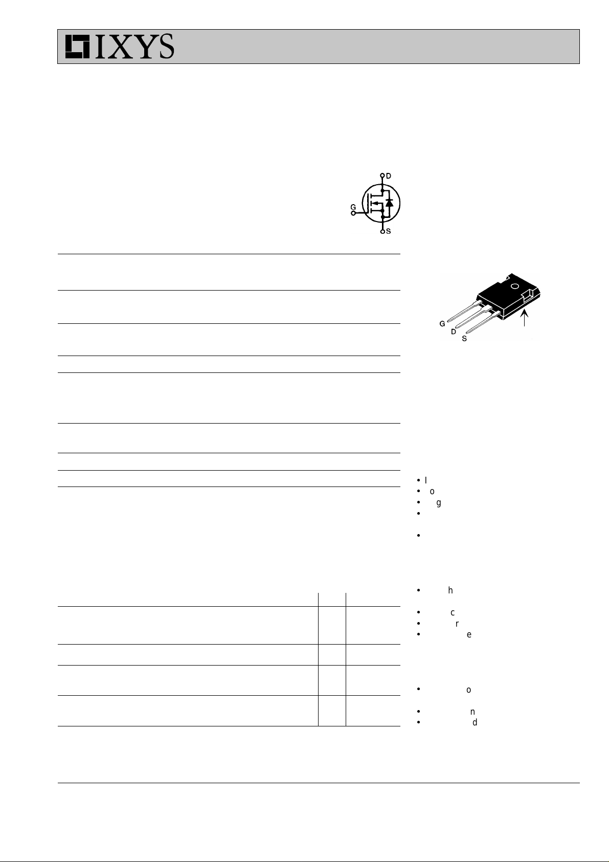
TO-247 AD
G = Gate, D = Drain,
S = Source, TAB = Drain
Max. lead temperature for soldering 300 °C
1.6 mm (0.063 in) from case for 10 s
M
d
Weight 6g
Mounting torque 1.13/10 Nm/lb.in.
Features
l
l
l
l
l
D (TAB)
International standard package
Low R
Rugged polysilicon gate cell structure
HDMOSTM process
DS (on)
Low package inductance (< 5 nH)
- easy to drive and to protect
Fast switching times
Symbol Test Conditions Characteristic Values
(TJ = 25°C, unless otherwise specified)
min. typ. max.
V
DSS
V
GS(th)
I
GSS
I
DSS
R
DS(on)
IXYS reserves the right to change limits, test conditions, and dimensions.
VGS= 0 V, ID = 3 mA 800 V
VDS= VGS, ID = 250 µA 2 4.5 V
VGS= ±20 VDC, VDS = 0 ±100 nA
VDS= 0.8 • V
VGS= 0 V TJ = 125°C1mA
DSS
VGS= 10 V, ID = 0.5 I
Pulse test, t ≤ 300 µs, duty cycle d ≤ 2 %
TJ =25°C 250 µA
D25
0.7 Ω
© 2000 IXYS All rights reserved
Applications
l
Switch-mode and resonant-mode
power supplies
l
Motor control
l
Uninterruptible Power Supplies (UPS)
l
DC choppers
Advantages
l
Easy to mount with 1 screw
(isolated mounting screw hole)
l
Space savings
l
High power density
96518F(12/97)
1 - 4
Page 2
IXTH 14N80
Symbol Test Conditions Characteristic Values
(TJ = 25°C, unless otherwise specified)
min. typ. max.
g
C
C
C
t
d(on)
t
r
t
d(off)
t
f
Q
Q
Q
R
R
fs
iss
oss
rss
g(on)
gs
gd
thJC
thCK
VDS= 10 V; ID = 0.5 • I
VGS= 0 V, VDS = 25 V, f = 1 MHz 310 pF
VGS= 10 V, VDS = 0.5 • V
RG = 2 Ω, (External) 63 100 ns
VGS= 10 V, VDS = 0.5 • V
, pulse test 8 14 S
D25
4500 pF
65 pF
20 50 ns
, ID = 0.5 I
DSS
D25
33 50 ns
32 50 ns
145 170 nC
, ID = 0.5 I
DSS
D25
30 45 nC
55 80 nC
0.42 K/W
0.25 K/W
Source-Drain Diode Characteristic Values
(TJ = 25°C, unless otherwise specified)
Symbol Test Conditions min. typ. max.
I
S
I
SM
V
SD
VGS= 0 V 14 A
Repetitive; pulse width limited by T
JM
56 A
IF = IS, VGS = 0 V, 1. 5 V
Pulse test, t ≤ 300 µs, duty cycle d ≤ 2 %
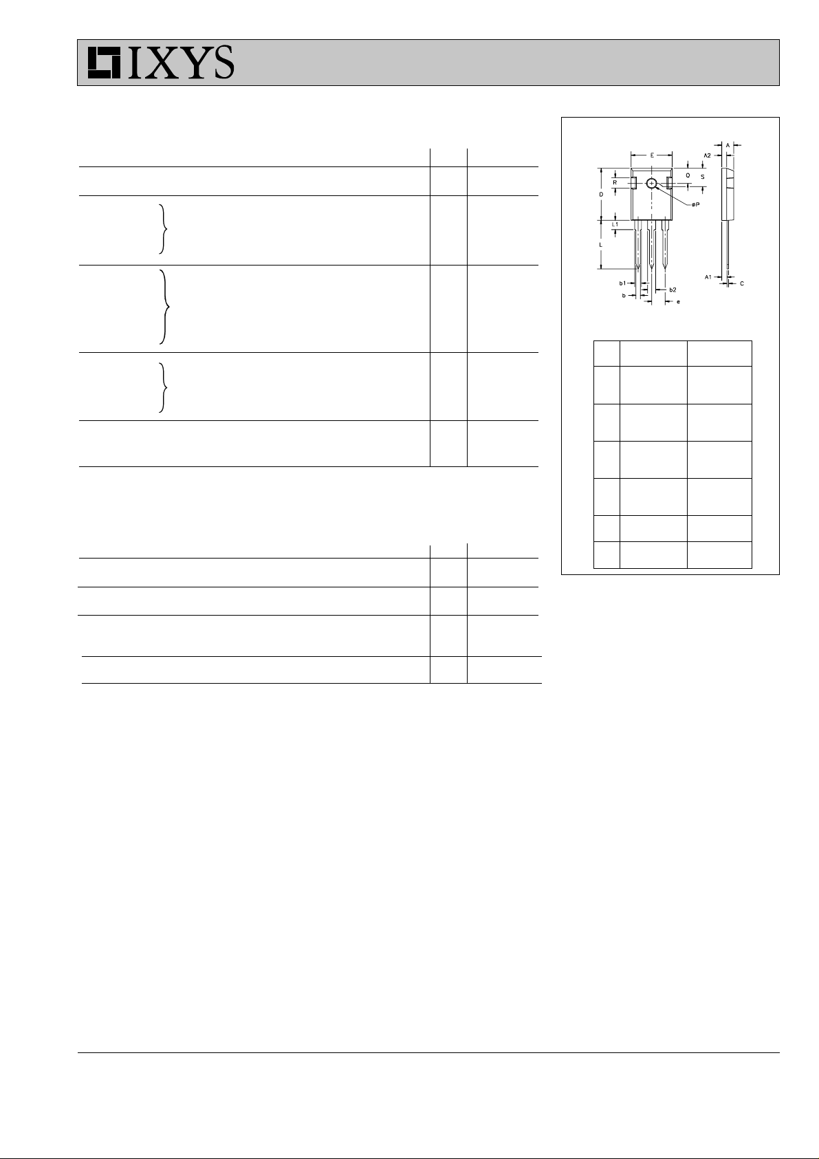
TO-247 AD Outline
1 2 3
Terminals: 1 - Gate 2 - Drain
3 - Source Tab - Drain
Dim. Millimeter Inches
Min. Max. Min. Max.
A 4.7 5.3 .185 .209
A
2.2 2.54 .087 .102
1
A22.2 2.6 .059 .098
b 1.0 1.4 .040 .055
b
1.65 2.13 .065 .084
1
b22.87 3.12 .113 .123
C .4 .8 .016 .031
D 20.80 21.46 .819 .845
E 15.75 16.26 .610 .640
e 5.20 5.72 0.205 0.225
L 19.81 20.32 .780 .800
L1 4.50 .177
∅P 3.55 3.65 .140 .144
Q 5.89 6.40 0.232 0.252
R 4.32 5.49 .170 .216
S 6.15 BSC 24 2 BSC
t
rr
IF = IS, -di/dt = 100 A/µs, VR = 100 V 800 ns
© 2000 IXYS All rights reserved
IXYS MOSFETS and IGBTs are covered by one or more of the following U.S. patents:
4,835,592 4,881,106 5,017,508 5,049,961 5,187,117 5,486,715
4,850,072 4,931,844 5,034,796 5,063,307 5,237,481 5,381,025
2 - 4
Page 3

IXTH 14N80
Figure 1. Output Characteristics at 25OC Figure 2. Output Characteristics at 125OC
20
16
12
8
- Amperes
D
I
4
0
0246810
Figure 3. R
2.6
2.4
2.2
2.0
1.8
1.6
- Normalized
1.4
DS(ON)
1.2
R
1.0
0.8
0 5 10 15 20 25
TJ = 25OC
VDS - Volts
normalized to 0.5 I
DS(on)
V
= 10V
GS
T
= 125OC
J
ID - Amperes
V
GS
8V
7V
6V
TJ = 25OC
= 9V
value vs. I
D25
5V
4V
20
= 125OC
T
J
16
V
= 9V
GS
8V
7V
6V
5V
12
8
- Amperes
D
I
4
4V
0
048121620
VDS - Volts
D
Figure 4. R
2.6
2.4
normalized to 0.5 I
DS(on)
V
= 10V
GS
value vs. T
D25
J
2.2
2.0
= 15A
I
1.8
- Normalized
1.6
DS(ON)
1.4
R
D
ID = 7.5A
1.2
1.0
25 50 75 100 125 150
TJ - Degrees C
Figure 5. Drain Current vs. Case Temperature Figure 6. Admittance Curves
20
16
12
8
- Amperes
D
I
4
0
-50 -25 0 25 50 75 100 125 150
TC - Degrees C
© 2000 IXYS All rights reserved
16
14
12
10
8
- Amperes
6
D
I
T
= 125oC
J
4
2
0
234567
VGS - Volts
T
= 25oC
J
3 - 4
Page 4

IXTH 14N80
Figure 8. Capacitance CurvesFigure 7. Gate Charge
12
V
= 400V
10
DS
= 15A
I
D
= 1mA
I
G
8
6
- Volts
GS
V
4
2
0
0 50 100 150 200 250
Gate Charge - nC
Figure 9. Source Current vs. Source to Drain Voltage
50
40
30
TJ = 125OC
20
- Amperes
D
I
10
TJ = 25OC
5000
Ciss
2500
f = 1MHz
1000
500
Coss
250
Capacitance - pF
100
Crss
50
0 5 10 15 20 25 30 35 40
VDS - Volts
Figure10. Forward Bias Safe Operating Area
100
10
- Amperes
D
I
1
TC = 25OC
0.1ms
1ms
10ms
100ms
DC
0
0.2 0.4 0.6 0.8 1.0 1.2 1.4
VSD - Volts
0.1
10 100 1000
V
- Volts
DS
Figure 11. Transient Thermal Resistance
1
D=0.5
0.1
D=0.2
- K/W
JC
R(th)
D=0.1
0.01
D=0.05
D=0.02
D=0.01
Single pulse
D = Duty Cycle
0.001
0.00001 0.0001 0.001 0.01 0.1 1 10
Pulse Width - Seconds
© 2000 IXYS All rights reserved
4 - 4
 Loading...