

High Speed IGBT
Short Circuit SOA Capability
V
CES
I
CES
t
fi
IXSH/IXST 30N60B 600 V 2.0 V 140 ns
IXSH/IXST 30N60C 600 V 2.5 V 70 ns
Symbol Test Conditions Maximum Ratings
V
CES
V
CGR
V
GES
V
GEM
I
C25
I
C90
I
CM
SSOA V
(RBSOA) Clamped inductive load, V
t
SC
(SCSOA) RG = 33 Ω, non repetitive
P
C
T
J
T
JM
T
stg
M
d
T
= 25°C to 150°C 600 V
J
T
= 25°C to 150°C; RGE = 1 MΩ 600 V
J
Continuous ±20 V
Transient ±30 V
T
= 25°C55A
C
T
= 90°C30A
C
T
= 25°C, 1 ms 110 A
C
= 15 V, T
GE
VGE= 15 V, VCE = 360 V, T
T
= 25°C 200 W
C
= 125°C, RG = 2.7 Ω I
J
= 0.8 V
CC
= 125°C 10µs
J
CES
@ 0.8 V
= 60 A
CM
CES
-55 ... +150 °C
150 °C
-55 ... +150 °C
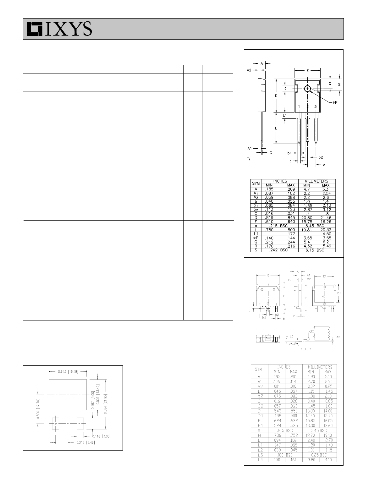
Mounting torque (TO-247) 1.13/10 Nm/lb.in.
Weight TO-247 6 g
TO-268 4 g
Maximum lead temperature for soldering 300 °C
1.6 mm (0.062 in.) from case for 10 s
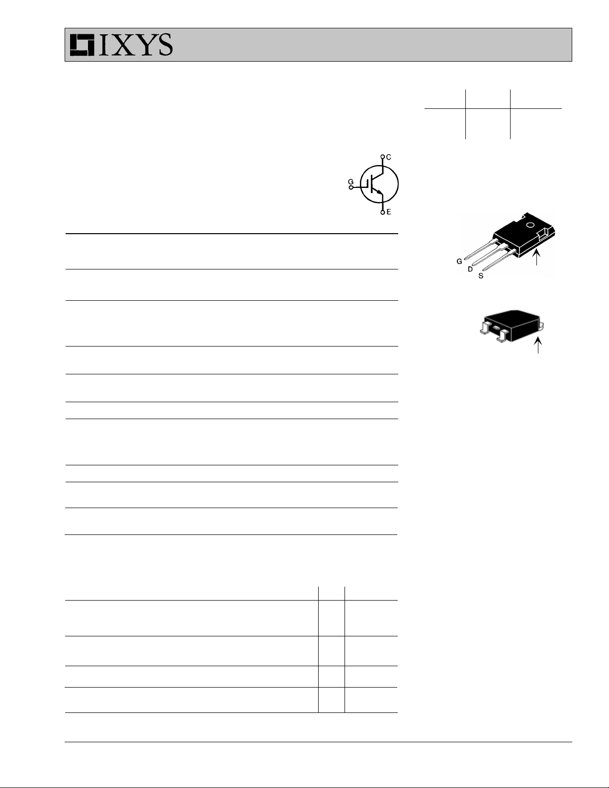
TO-247 AD (IXSH)
TO-268 (D3) ( IXST)
G
S
G = Gate
S = Source TAB = Drain
Features
l
International standard packages
l
Short Circuit SOA capability
l
High frequency IGBT
l
New generation HDMOS
TM
process
Applications
(TAB)
(TAB)
Symbol Test Conditions Characteristic Values
(T
= 25°C, unless otherwise specified)
BV
V
I
CES
I
GES
V
CES
GE(th)
CE(sat)
I
= 250 µA, V
C
IC= 2.5 mA, VCE = V
VCE= 0.8 V
VGE= 0 V T
VCE= 0 V, V
VGE= 15 V; IC = I
© 2001 IXYS All rights reserved
J
= 0 V 600 V
GE
GE
T
CES
= ±20 V ±100 nA
GE
C90
= 25°C 100 µA
J
= 125°C1mA
J
30N60B 2.0 V
30N60C 2.5 V
min. typ. max.
47V
l
AC motor speed control
l
DC servo and robot drives
l
DC choppers
l
Uninterruptible power supplies (UPS)
l
Switch-mode and resonant-mode
power supplies
Advantages
l
Easy to mount with 1 screw
(isolated mounting screw hole)
l
Surface mountable, high power case
style
l
Reduce assembly time and cost
l
High power density
98519B (11/01)
IXSH/IXST 30N60B
IXSH/IXST 30N60C
Symbol Test Conditions Characteristic Values
(T
= 25°C, unless otherwise specified)
g
C
C
C
Q
Q
Q
t
t
t
t
E
t
t
E
t
t
E
fs
ies
oes
res
g
ge
gc
d(on)
ri
d(off)
fi
off
d(on)
ri
on
d(off)
fi
off
J
IC = I
Pulse test, t ≤ 300 µs, duty cycle ≤ 2 %
; VCE = 10 V, 10 S
C90
VCE = 25 V, VGE = 0 V, f = 1 MHz 240 pF
IC = I
Inductive load, TJ = 25
I
C
VCE= 0.8 V
Note 1
Inductive load, TJ = 125
I
C
VCE= 0.8 V
Note 1
, VGE = 15 V, VCE = 0.5 V
C90
°°
°C
°°
= I
, VGE = 15 V
C90
, R
= 4.7 Ω
CES
G
= I
, VGE = 15 V
C90
, R
= 4.7 Ω
CES
G
°°
°C
°°
CES
min. typ. max.
3100 pF
30 pF
100 nC
30 nC
38 nC
30 ns
30 ns
30N60B 150 270 ns
30N60C 90 150 ns
30N60B 140 270 ns
30N60C 70 120 ns
30N60B 1.5 2.5 mJ
30N60C 0.7 1.2 mJ
35 ns
35 ns
0.5 mJ
30N60B 270 ns
30N60C 150 ns
30N60B 250 ns
30N60C 140
30N60B 2.5 mJ
30N60C 1.2 mJ
TO-247 AD Outline
1 = Gate
2 = Collector
3 = Emitter
Tab = Collector
TO-268 Outline
R
thJC
R
thCK
(TO-247) 0.25 K/W
Notes: 1. Switching times may increase for VCE (Clamp) > 0.8 V
increased RG.
0.62 K/W
, higher TJ or
CES
Min Recommended Footprint
IXYS reserves the right to change limits, test conditions, and dimensions.
IXYS MOSFETS and IGBTs are covered by one or more of the following U.S. patents: 4,835,592 4,881,106 5,017,508 5,049,961 5,187,117 5,486,715
4,850,072 4,931,844 5,034,796 5,063,307 5,237,481 5,381,025

IXSH/IXST 30N60B
IXSH/IXST 30N60C
Fig.1 Saturation Characteristics Fig.2 Output Characterstics
100
80
TJ = 25°C
VGE = 15V
13V
200
160
TJ = 25°C
VGE = 15V
13V
11V
60
11V
40
- Amperes
C
I
9V
20
7V
0
012345
VCE - Volts
120
80
- Amperes
C
I
40
0
0246810
VCE - Volts
9V
7V
5V
Fig.3 Collector-Emitter Voltage Fig.4 Temperature Dependence
vs. Gate-Emitter Voltage of Output Saturation Voltage
120
TJ = 125°C
VGS=15V
100
80
60
- Amperes
C
40
I
20
0
0246810
VCE - Volts
13V
11V
9V
7V
1.6
= 60A
VGE = 15V
I
C
1.4
1.2
= 30A
I
C
- Normalized
1.0
CE (sat)
V
0.8
IC = 15A
0.6
25 50 75 100 125 150
TJ - Degrees C
Fig.5 Input Admittance Fig.6 Temperature Dependence of
140
120
100
- Amperes
C
I
V
= 10V
CE
80
60
T
= 125°C
40
J
20
0
4 6 8 10121416
VGE - Volts
© 2001 IXYS All rights reserved
TJ = 25°C
Capacitance - pF
Breakdown and Threshold Voltage
10000
1000
100
10
0 5 10 15 20 25 30 35 40
VCE-Volts
C
C
oss
C
f = 1Mhz
iss
rss

IXSH/IXST 30N60B
IXSH/IXST 30N60C
Fig.7 Turn-Off Energy per Pulse and Fig.8 Dependence of Turn-Off Energy
1.5
Fall Time on Collector Current Per Pulse and Fall Time on R
TJ = 125°C
RG = 10Ω
1.0
- millijoules
E
(ON)
0.5
E
(ON)
E
(OFF)
0.0
0 20406080
IC - Amperes
Fig.9 Gate Charge Characteristic Curve Fig.10 Turn-Off Safe Operating Area
7.5
5.0
2.5
0.0
(OFF)
2.0
TJ = 125°C
E
1.5
E
(OFF)
IC = 60A
- milliJoules
1.0
- millijoules
(ON)
E
0.5
0.0
E
(ON)
I
C
= 15A
I
C
= 30A
0 1020304050
RG - Ohms
G
E
(ON)
8
E
6
(OFF)
- millijoules
(OFF)
(OFF)
4
2
0
E
(ON)
E
E
15
12
V
I
C
CE
=30A
= 300V
9
- Volts
GE
6
V
3
0
0 25 50 75 100 125
Qg - nanocoulombs
Fig.11 Transient Thermal Impedance
1
D=0.5
D=0.2
0.1
D=0.1
D=0.05
(K/W)
D=0.02
thJC
D=0.01
Z
0.01
D = Duty Cycle
100
10
- Amperes
C
1
I
TJ = 125°C
RG = 4.7Ω
dV/dt < 5V/ns
0.1
0 100 200 300 400 500 600
VCE - Volts
Single pulse
0.001
0.00001 0.0001 0.001 0.01 0.1 1
Pulse Width - Seconds
IXYS reserves the right to change limits, test conditions, and dimensions.
IXYS MOSFETS and IGBTs are covered by one or more of the following U.S. patents: 4,835,592 4,881,106 5,017,508 5,049,961 5,187,117 5,486,715
4,850,072 4,931,844 5,034,796 5,063,307 5,237,481 5,381,025
 Loading...