

Datasheet ISR2805DURH, ISR2805DSRH, ISR2805DKURH, ISR2805DKSRH, ISR2800DKSRH Datasheet (MSK)
...Page 1

4704 Dey Road Liverpool, N.Y. 13088 (315) 701-6751
M.S.KENNEDY CORP.
ISO 9001 CERTIFIED BY DSCC
ISR2800D
RADIATION HARDENED
HIGH-POWER, HIGH EFFICIENCY
DC-DC POWER CONVERTER
DESCRIPTION:
The ISR2800D is the first in a series of radiation-hardened, high-reliability power supplies to be offered by MSK.
The ISR2800D is specifically optimized to drive transmit/receive (T/R) modules in Phased Array Antennas (PAA), but
as a result of its high-performance capabilities and numerous built-in features, it is ideal for many other applications.
The ISR2800D utilizes two DC-DC converters to optimize power conversion efficiency and facilitate voltage sequenc-
ing necessary to protect T/R modules during power-up and power-down. A small flyback converter, referenced to
input return and switching at 200kHz, is used to provide electrical input-output isolation, generate nominal +10VDC
bias voltages for the input and output control circuits of the power supply, and generate a nominal -5VDC negative
output voltage for the T/R modules. The negative output voltage for the T/R modules is cross-regulated via a tap on
the flyback transformer and referenced to output return. A low drop-out (LDO) linear regulator is then used to further
post-regulate this output voltage to ensure tight regulation and low ripple, typically less than 5mVp-p. A single
transistor forward converter, referenced to output return and switching at 100kHz, provides the positive adjustable
output voltage. They are enclosed in a hermetic Silicon Aluminum (SiAl) package and weigh less than TBD grams.
The package utilizes rugged ceramic feed-through Glid-Cop pins and is sealed using parallel seam welding.
FEATURES:
82.5W Output Power
18-40VDC Steady-state Input Voltage Range
Adjustable Positive Output Voltage - 3.3V to 5.0V
Fixed -5V Negative Output
Typical 90% Efficiency from Half Load to Full Load
Total Dose - 100krad(Si)(max)
Single-Event Effects - LET>82MeV-cm²/mg
SEGR Hardened MOSFETs
Integrated Circuits are SEL Immune
Internal EMI Filter meets MIL-STD-461
Input Inrush Current Limiting
Remote Sense for Main Output Voltage
Soft-start Circuitry Prevents Output Voltage Overshoot
Input Undervoltage Lockout
Output Overload and Short Circuit Protection
Output Overvoltage Protection
Synchronization Capability
External Inhibit
1
Rev. - 3/01
PRELIMINARY
TYPICAL APPLICATIONS
Geostationary (GEO) Earth Orbit Satellites
Low Earth Orbit (LEO) Satellites
Deep Space Satellites/Probes
Communication Systems
PIN-OUT INFORMATION
CROW BAR
-5V OUT
VOUT RTN
+VOUT
VOUT RTN
+VOUT
VOUT RTN
+VOUT
VOUT RTN
+VOUT
REM SENSE
VOUT ADJ
VOUT OVP ADJ
PRI INHIBIT
ETERM
INPUT
INPUT RTN
INPUT
INPUT RTN
INPUT
INPUT RTN
INPUT
INPUT RTN
SEC ON/OFF
SYNC OUT
SYNC IN
1
2
3
4
5
6
7
8
9
10
11
12
13
14
15
16
17
18
19
20
21
22
23
24
25
26
Page 2
2
-0.5V to +50V
Internally Limited
-0.5V to +50V
-0.5V to +50V
-0.5V to +5.0V
+Vout ±0.5V
+300°C for 10 seconds
-55°C to 85°C
-55°C to 150°C
Input Voltage Range
Ouput Power
PRI Inhibit
Sec On/Off
Sync In
Rem Sense
Lead Temperature
Operating Temperature
Storage Temperature
ABSOLUTE MAXIMUM RATINGS
○○○○○○○○○○○
○○○○○○○○○○○○○○○
○○○○○○○○○○
○○○○○○○○
○○○○○○○○○○
Rev. - 3/01
PRELIMINARY
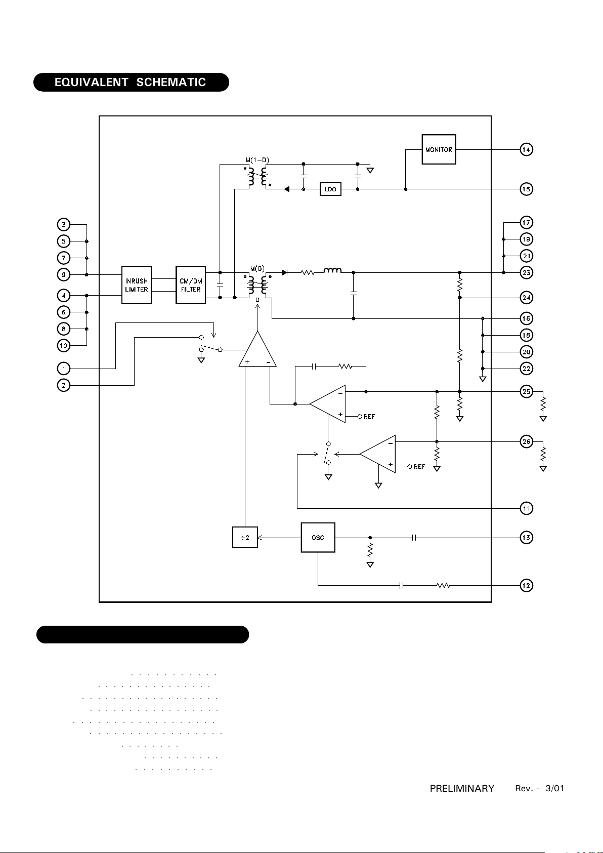
EQUIVALENT SCHEMATIC
○○○○○○○○○○○○○○○○○
○○○○○○○○○○○○○○○○○○
○○○○○○○○○○○○○○○○○
○○○○○○○○○○○○○○○○○○
Page 3
3
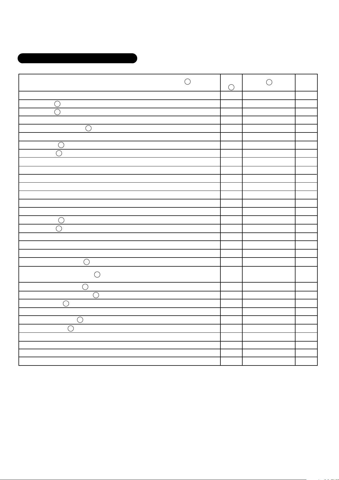
INPUT CHARACTERISTICS
Input Voltage
Input Voltage
-5VOUT
Output Converter Frequency
Output Voltage
Output Current
Output Power
Output Ripple
Output Current Limit
Output Over-voltage Limit
+VOUT
Output Converter Frequency
Output Voltage Adjustable Range
Output Voltage Regulation
Output Current
Output Power
Output Ripple
Output Current Limit
Output Over-voltage Limit
Output Step-load Response
Output Step-line Response
Output Step-line Recovery Time
Output Efficiency
+VOUT
Power Supply Efficiency
TURN-ON RESPONSE
-5VOUT Output Overshoot
-5VOUT Output Turn-on Time
+VOUT Overshoot
+VOUT Turn-on Time
Max.
40
50
240
-4.75
500
2.5
10
1.75
-5.50
115
5.00
5.0
-
80
1.0
24.0
130
1.6
1.6
50
-
-
-
200
-
500
Typ.
28
-
200
-5.00
200
1
5
1.50
-6.00
100
-
0.0
-
-
0.4
21.3
120
0.8
0.8
-
90
89
0
-
0
-
Min.
18
-0.5
160
-5.25
-
-
-
1.25
-6.50
85
3.30
-5.0
16
-
-
16.0
110
-1.6
-1.6
-
86
85
-
-
-
-
V
V
KHz
V
mA
W
mVp-p
A
V
KHz
V
%Vo
A
W
%Vo-p-p
A
%Vo
%Vo-p
%Vo-p
uS
%
%
mV
mS
mV
mS
Steady-state
Transient, ≤ 50ms
Zero Load to/from Half Load, VIN=22-40VDC
Zero Load to/from Half Load, VIN=22-40VDC
Recovery to within ±1% of VOUT
18V to/from 40V
18V to/from 40V, Recovery to within 1% of VOUT
+VOUT=5V, IOUT=8-16A; -IOUT=-200mA
+VOUT=5V, IOUT=16A; -IOUT=-500mA
Input Voltage Stepped from 0 to 28VDC
Parameter
Units
ISR2800D
Test Conditions
Group A
Subgroup
1,2,3
1,2,3
4,5,6
1,2,3
1,2,3
1,2,3
4,5,6
1,2,3
1,2,3
4,5,6
1,2,3
1,2,3
1,2,3
1,2,3
4,5,6
1,2,3
1,2,3
4,5,6
4,5,6
4,5,6
1,2,3
1,2,3
-
4,5,6
-
4,5,6
ELECTRICAL SPECIFICATIONS
Rev. A 10/99
PRELIMINARY
Output Step-load Recovery Time
4,5,6
Continued on next page
-
-50
uS
1
4
5
2
3
2
3
2
2
2
3
3
3
3
3
3
3
Page 4

4
ELECTRICAL SPECIFICATIONS CONTINUED
Rev. - 3/01
PRELIMINARY
NOTES:
1 -55°C ≤ Tc ≤ 85°C, V
IN=18-40VDC, IOUT-MAIN=0-16A, IOUT-AUX=0-500mA, unless otherwise specified
2 This parameter is an operating condition and is verified during device testing.
3 This parameter shall be guaranteed by design and need not be tested.
4 Typical parameters are representative of actual device performance but are for reference only.
5 Subgroup 1,4 TA=TC=+25°C
2,5 T
A=TC=+125°C
3,6 T
A=TC=-55°C
PRI INHIBIT INPUT
Input Voltage Range
Open Circuit Voltage
Input (Sink) Current
SEC ON/OFF
Input Voltage Range
Open Circuit Voltage
Input (Sink) Current
POWER DISSIPATION
Load Fault
PRI Input Inhibit Active
Sec Output Inhibit Active
MISC
Line Rejection
Isolation
Unit Weight
CAPACITIVE LOAD
-5VOUT
+VOUT
SHORT CIRCUIT RECOVERY TIME
-5VOUT
+VOUT
SYNC OUT
Amplitude
SYNC IN
Input Threshold
Frequency Range
Input Current
Min Pulse Width
CROW BAR
Output High Voltage
Output High Current
Max.
50
18
2
50
12
2.5
10
0.05
2
-
-
TBD
TBD
288
200
500
5.0
-
400
75
500
12
20
Typ.
-
-
-
-
-
-
-
-
-
60
-
-
-
-
-
-
-
-
-
-
-
-
V
V
mA
V
V
mA
W
W
W
dB
MΩ
grams
µF
µF
mS
mS
V
V
KHz
mA
nS
V
mA
Main Output Short Circuit
IOUT=0A
DC to 50KHz
Input to Output, Input to Case, Output to Case Tested at 100VDC
No effect on DC Performance.
Outputs returns to within 1% of nominal voltage
IOUT≤10mA
VSYNC=3.5V
Parameter
Units
ISR2800D
Test Conditions
Group A
Subgroup
1,2,3
1,2,3
1,2,3
1,2,3
1,2,3
1,2,3
1,2,3
1,2,3
1,2,3
4,5,6
1
-
-
-
4
4
1,2,3
1,2,3
4,5,6
1,2,3
4,5,6
1,2,3
1,2,3
Min.
-0.5
9
-
-0.5
6
-
-
-
-
40
100
-
-
-
-
3.5
3.5
250
-
20
9
10
2
4
5
2
3
3
3
3
3
3
3
Page 5

5
Rev. - 3/01
PRELIMINARY
PRI INHIBIT - Allows on/off control from circuits referenced to the input return. Main and auxiliary outputs
are on when this pin is left open and off when this pin is shorted to input return.
ETERM - Allows control of PRI Inhibit pin in electrically noisy environments. This pin bypasses the internal
EMI filter to the internal ground reference and must be isolated. Connecting this pin to the PRI inhibit will
disable the unit.
INPUT - Input power terminals to connect to primary power source. All of these pins must be connected by
the user.
INPUT RTN - Input power terminals to connect to primary power source. All of these pins must be con-
nected by the user.
SEC ON/OFF - Allows on/off control from circuits referenced to the output return. +Vout and -5Vout
outputs are on when this pin is left open. +Vout is off when this pin is shorted to output return.
SYNC OUT - Allows user to synchronize other devices to the operating frequency of the converter. This AC
coupled pin can drive up to 50Ω with an output level of 3.4V.
SYNC IN - Allows user control of the converter operating frequency within a limited range. If unused,
connect to output return, or leave open. This pin has an input impedance of 50Ω.
CROW BAR - Allows user control to ensure proper voltage sequencing during fault conditions. This com-
mand may be used to activate a crowbar circuit on the main output to guarantee proper power down
sequencing. This output should normally be buffered (e.g. to drive the gate of a FET) in timing critical
sequencing applications. For non-critical timing or high impedance input devices, it may be used directly.
Otherwise, it should be left open.
-5VOUT - Provides 2.5W of negative five volt, low noise bias power.
SEC RTN - Output power return terminals to connect to isolated secondary loads. This is the return ground
reference for both the outputs. All of these pins must be connected by the user.
+VOUT - Main adjustable output voltage. Output power terminals connect to isolated secondary loads.
This output is adjustable from 3.3V to 5V. All of these pins must be connected by the user.
REM SENSE - Remote sense allows user to connect to a remote location near the load for point of regulation.
This overcomes a limited amount of voltage drop in the distribution network. Otherwise, connect this pin to
the +Vout output.
VOUT ADJ - Allows adjustment of the +Vout voltage over the allowable range using an external resistor
from this pin to the output return.
VOUT OVP ADJ - Allows adjustment of the over-voltage protection (OVP) threshold to match the (adjust-
able) main output voltage. Threshold is adjusted by connecting a resistor from this pin to the output return.
APPLICATION NOTES
ISR2800D PIN DESCRIPTIONS
Page 6

6
Rev. - 3/01
PRELIMINARY
APPLICATION NOTES CONT'D
BASIC ARCHITECTURE:
MSK power converters utilize two DC-DC converters to opti-
mize power efficiency and to provide internal housekeeping power
while magnetically isolating the power bus from the load. A small
flyback converter, referenced to input return, is used to provide
electrical input-output isolation and will generate nominal +10VDC
bias voltages for the input and output control circuits of the power
supply. A single transistor forward converter, referenced to out-
put return, provides the main output voltage.
FLYBACK CONVERTER:
The flyback converter uses peak current-mode Pulse Width
Modulator (PWM) control and operates in discontinuous conduc-
tion-mode. Regulation is achieved by sampling the input bias volt-
age directly and feeding it back to the control circuit of the flyback
converter, which is referenced to input return.
FORWARD CONVERTER:
The forward converter uses voltage Mode Pulse Width Modu-
lator (PWM) control with input voltage feed-forward and operates
in continuous conduction-mode. Regulation is achieved by sam-
pling the output voltage directly and feeding it back to the control
circuit of the forward converter, which is referenced to output
return. Since the main output voltage is directly regulated without
the use of magnetically-coupled feedback, superior voltage regula-
tion can be achieved. A single-stage L-C output filter reduces the
typical output ripple to less than 25mVp-p.
SYNCHRONOUS RECTIFICATION:
Synchronous rectification is used to achieve high-conversion
efficiency over a half to full output load range and allows con-
verter operation in continuous conduction-mode down to zero out-
put load. This capability results in far superior dynamic perfor-
mance when the load is stepped to or from a zero load condition,
and is particularly critical in pulsed Phased Array Antenna and
modern microprocessor applications which have high peak current
demands and fast load transients.
INPUT EMI FILTER:
The input EMI filter is comprised of a multi-stage L-C filter
which provides attenuation of the differential-mode emissions from
the power supply. A balun, in conjuction with very small line-to-
chassis and return-to-chassis capacitors, provides attenuation of
the common-mode emissions from the power supply. Together
these components enable the power supply to meet the conducted
emission requirements of MIL-STD-461.
INRUSH CURRENT LIMITING:
Inrush current limiting circuitry limits initial peak input charg-
ing current at turn-on to less than two times maximum steady-
state input current. Consequently, even when the input voltage to
the power supply is instantaneously stepped, peak charging cur-
rent is well controlled.
UNDERVOLTAGE LOCKOUT:
An undervoltage lockout circuit prevents the power supply from
operating when the input line voltage is too low to maintain the
output voltage. The converter will not start until the line voltage
rises to approximately 17V and will shut down when the input
voltage drops below approximatley 16V. The approximate 1V of
hysteresis reduces the possibility of line noise interfereing with
the converter during power-up and power-down.
SOFT-START:
Soft-start circuitry associated with both the flyback and for-
ward converters is guaranteed to prevent output voltage over-
shoot during power-up for both the auxiliary and main output volt-
ages.
USER-ADJUSTABLE MAIN OUTPUT:
The +VOUT output voltage is user-adjustable over a range of
3.3VDC to 5VDC. Setting the positive output voltage is accom-
plished by using a single external resistor. The output voltage
may be programmed by the user to any desired voltage within this
range. The table below shows the value of resistance necessary
to set several common output voltages. The equation below may
be used to determine the resistor value required for other set points.
The output voltage may be adjusted up to 6V and down to 3V, but
some performance specifications will not be met.
Output Voltage Adjust Resistor Value (in KΩ)
f(Vout) = -6.7
f(3.0) = 2.98 x 10³
f(3.3) = 141.95
f(5.0) = 8.22
f(5.2) = 5.97
OVERVOLTAGE PROTECTION (OVP):
Overvoltage protection is provided for both the negative and
positive output voltages of the power supply. The overvoltage
protection circuit for the negative output voltage limits peak volt-
age to approximately 120% of nominal. The overvoltage limit for
the positive output voltage is programmable with a single external
resistor. It is recommended that this overvoltage limit be set at
approximately 120% of nominal.
The overvoltage protection is programmable over a limited range
using only a single external resistor. The OVP voltage may be
programmed by the user to any desired voltage within this range.
The OVP set point should be coordinated with the positive output
voltage and set to approximately 110% to 120% of the nominal
output. The table below shows the value of resistance necessary
to set the OVP to 120% for several common output voltages. The
equation below may be used to determine the resistor value re-
quired for other set points.
Output Voltage Over-Voltage Protection (OVP) Adjust Resistor Value
(in KΩ)
g(OVP) = -3.44
g(3.6) = 238.12
g(3.96) = 22.51
g(6) = 0.84
g(6.24) = 0.46
VOLTAGE SEQUENCING:
Output voltage sequencing is provided to protect T/R modules
from damage when used in PAA applications. During power-up,
the positive output voltage remains off until the negative output
voltage has reached normal regulation limits. During power-down,
a crowbar command is available to ensure that the positive output
voltage falls to 10% or less of its steady state value before the
negative output voltage falls more than 20% from its nominal value.
During fault mode the crowbar command allows user control of
the crowbar circuit on the positive output to ensure proper voltage
sequencing for application specific requirements.
2.5
0.04975Vout-0.1484166
10.4667
OVP-3.55667
Page 7

7
Rev. - 3/01
PRELIMINARY
APPLICATION NOTES CONT'D
RADIATION PERFORMANCE
MSK converters give you superior radiation performance with-
out the highs and lows of using "typical" DC-DC converters. The
design represents a break from the traditional hardening method
of simply replacing commercial die elements with radiation screened
die in an off-the-shelf DC-DC converter design.
Special design techniques implemented at both the module
level and the transistor circuit element level were used to harden
the DC-DC converters. Here are some of the engineering steps
taken to guarantee the radiation performance.
TOTAL DOSE HARDNESS:
The converters employ a fully magnetically-isolated configura-
tion allowing the positive converter output to be regulated directly
without the use of opto-couplers. Galvanic isolation between in-
put and output is provided by the flyback converter and a small
gate-drive transformer which couples the PWM drive signal to the
main switching MOSFET. This approach provides optimum out-
put voltage regulation and avoids the gain degrading effects of
total ionizing dose on opto-couplers which can result in converter
failure.
SINGLE-EVENT EFFECTS HARDNESS:
All critical ICs in the converter use a latch-up immune,
dielectrically-isolated, BiCMOS process that prevents converter
components from entering a potentially catastrophic latched state.
The heart of the DC-DC converter is the Single-Event Effects
hardened PWM. The chip has SEU-immune CMOS soft-start con-
trol logic which will not upset in a heavy ion environment. The on-
chip overcurrent comparator employs a redundant cross-checking
comparator design. Error amp circuitry incorporates redundant
wire OR differential input stages which prevent the amplifier out-
put from over-ranging, which could cause excessive output pulse
widths leading to overcurrent fault sequencing, transformer core
saturation or power switch overstress. The toggle Flip/Flop (F/F)
and all pulse control logic functions have been designed in SEU-
immune CMOS to keep pulse phase integrity from being upset.
The PWM used in the flyback circuitry incorporates these
same improvements with the exception of the soft-start func-
tion.
DC-DC converters use comparator ICs to control various
converter functions such as input inrush current limiting, input
undervoltage lockout, start-up regulator shutdown, output ov-
ervoltage protection, and main/auxiliary output voltage sequenc-
ing. A high-energy ion striking the comparator can cause any
of these functions to fail or inadvertantly activate causing un-
wanted power supply interruptions. The MSK converters em-
ploy a new hardened, SEU immune, quad comparator. The
chip uses triple redundant bipolar comparators for analog preci-
sion, and is backed by SEU-immune voting logic which ensures
that no single-particle error can propagate to the output.
The potential for catastrophic single-event gate rupture in
MOSFET's has led to the development of MOSFET's with ox-
ide structures which resist breakdown up to fully rated MOSFET
voltage potential under fully off-biased conditions. All MOSFET's
used in the converters mitigate Single-Event Gate Rupture ef-
fects up to 82 MeV-cm²/mg.
A PROVEN DESIGN METHODOLOGY
The power supplies were developed using a proven, conserva-
tive design methodology which includes selecting radiation-hard-
ened and established reliability components and fully de-rated to
the requirements of MIL-STD-975, MIL-STD-1547 and GSFC PPL-
21 Appendix B. Proprietary radiation-hardened silicon gate (RSG)
process for integrated circuits ensures total dose capability to
300krads and immunity to single-event latch-up (SEL). Radiation-
hardened power MOSFETs virtually eliminate the possibility of
single-event gate rupture and single-event burn-out. Direct regu-
lation is utilized instead of opto-couplers to minimize temperature,
radiation and aging sensitivity. The Cadence Analog Work Bench
(AWB) tool set, including Sensitivity/Worst Case and Monte Carlo
tools, was used extensively to predict and optimize circuit perfor-
mance for both beginning and end-of-life. Thorough design analy-
sis include Worst Case, Component Stress and Reliability (MTBF).
MSK's DC-DC converters offer high reliability through "tried
and true" methods of passive component procurement and hybrid
construction techniques. All stacked capacitors are procured, pre-
assembled (stacked) and up screened by the capacitor manufac-
turer. Capacitor mounting procedures are performed per the
supplier's guidelines. Magnetics, resistors and capacitors are all
procured to the highest standards. Full component level traceabil-
ity is maintained on all high-rel lots. Final hybrid assembly and
screening is available up to MIL-PRF-38534 Class K or Class H
requirements.
Page 8

8
Rev. - 3/01
PRELIMINARY
TYPICAL SYSTEM OPERATION
A typical application shows the ISR2805DSKE connections to an arbitrary load. The remote
sense line is used to eliminate voltage drop in the positive distribution lead. The negative output
provides bias to hold the gate of FET drive transistors off in radiation environments. A FET crowbar
circuit is driven directly to discharge the filter capacitance at the load during shutdown. The two
resistors connected to the OVP and VOUT ADJ pins set the output over voltage limit and output
voltage to the required values. Also illustrated is a connection to synchronize two converters to a
master clock. An isolated connection is shown to inhibit both converter outputs from the primary
referenced input voltage as well as a secondary ON/OFF command referenced to the output to
shutdown the positive output.
Page 9

9
The information contained herein is believed to be accurate at the time of printing. MSK reserves the right to make
changes to its products or specifications without notice, however, and assumes no liability for the use of its products.
Please visit out website for the most recent revision of this datasheet.
MECHANICAL SPECIFICATIONS
M.S. Kennedy Corp.
4704 Dey Road, Liverpool, New York 13088
Phone (315) 701-6751
FAX (315) 701-6752
www.mskennedy.com
ISR2800DKSRH
The above example is a Class K adjustable dual output rad-hard converter
RAD-HARD
LEAD CONFIGURATIONS
S= STRAIGHT; U= BENT UP; D= BENT DOWN
SCREENING
BLANK= INDUSTRIAL; E= EXTENDED RELIABILITY;
H= CLASS H; K= CLASS K
DUAL OUTPUT
OUTPUT VOLTAGE
+ADJ/-5V
NOMINAL INPUT VOLTAGE
GENERAL PART NUMBER
ORDERING INFORMATION
NOTE: ALL DIMENSIONS ARE ±0.010 INCHES UNLESS OTHERWISE LABELED.
ESD Triangle indicates Pin 1.
Rev. - 3/01
PRELIMINARY
 Loading...