

Page 1
Data Sheet June 2002
ISL9N2357D3ST
30V, 0.007 Ohm, 35A, N-Channel
UltraFET
UltraFET® Trench from Fairchild is a new advanced
MOSFET technology that achieves the lowest possible onresistance per silicon area while maintaining fast switching
and low gat e charge. The reduced c onduction and s wi tching
losses extend battery life in notebook PCs, cellular
telephones and other portable information appliances and
improve the overall efficiency of high frequency DC-DC
converters used to power the latest microprocessors.
®
Trench Power MOSFET
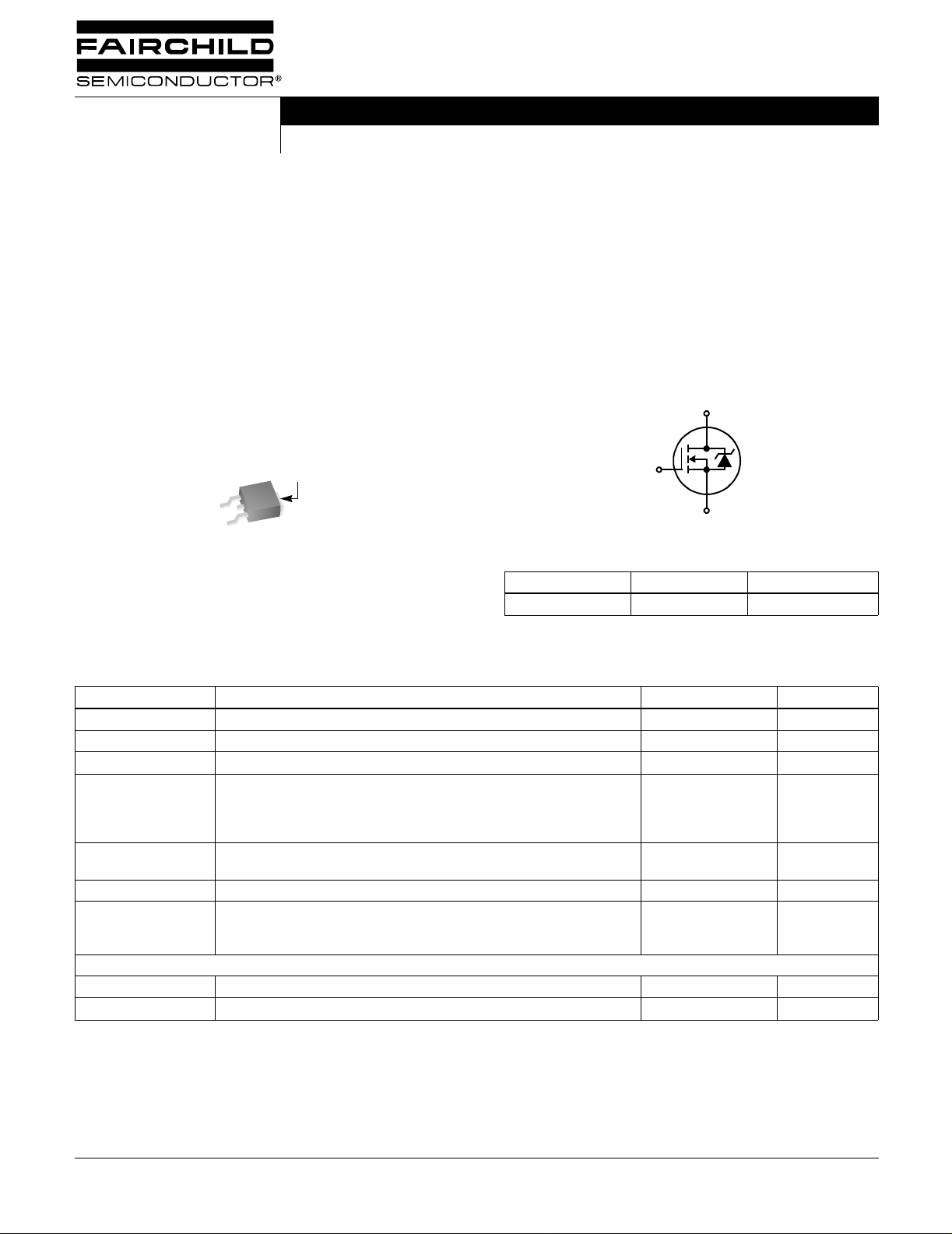
Packaging
ISL9N2357D3ST
JEDEC TO-252AA
DRAIN (FLANGE)
GATE
SOURCE
UltraFET® Trench
Features
•r
•Q
•Q
•C
Symbol
Ordering Information
ISL9N2357D3ST TO-252AA N2357D
NOTE: When ordering, use the entire part number.
e.g., ISL9N2357D3ST.
= 0.006Ω Typical, V
DS(ON)
Total 85nC Typical, VGS = 10V
g
16nC Typical
gd
5600pF Typical
ISS
G
PART NUMBER PACKAGE BRAND
D
S
GS
= 10V
Absolute Maximum Ratings T
SYMBOL PARAMETER ISL9N2357D3ST UNITS
V
DSS
V
DGR
V
GS
I
D
I
D
I
DM
P
D
T
, T
J
STG
T
L
T
pkg
THERMAL SPECI FICATIONS
R
θJC
R
θJA
NOTE:
1. T
= 25oC to 150oC.
J
CAUTION: Stresses above those listed in “ Absolute M aximum Ratings” may cause perm anent damage to the device. This is a stre ss only rating and operation of the
device at these or any other conditions above those indicated in the operational sections of this specification is not implied.
Drain to Source Voltage (Note 1) 30 V
Drain to Gate Voltage (RGS = 20kΩ) (Note 1) 30 V
Gate to Source Voltage ±20 V
Drain Current
Continuous (T
Continuous (T
Pulsed Drain Current
Power Dissipation
Derate Above 25
Operating and Storage Temperature -55 to 175
Maximum Temperature for Soldering
Leads at 0.063in (1.6mm) from Case for 10s
Package Body for 10s, See Techbrief TB334
Thermal Resistance Junction to Case, TO-252 1.5
Thermal Resistance Junction to Ambient TO-252 100
= 25oC, Unless Otherwise Specified
C
= 25oC, VGS = 10V) (Figure 2)
C
= 100oC, VGS = 10V)
C
o
C
35
35
Figure 4
100
0.67
300
260
A
A
A
W
W/oC
o
C
o
C
o
C
o
C/W
o
C/W
©2002 Fairchild Semiconductor Corporation ISL9N2357D3ST Rev. B1
Page 2

ISL9N2357D3ST
Electrical Specifications T
= 25oC, Unless Otherwise Specified
C
PARAMETER SYMBOL TEST CONDITIONS MIN TYP MAX UNITS
OFF STATE SPECIFICATIONS
Drain to Source Breakdown Voltage BV
Zero Gate Voltage Drain Current I
Gate to Source Leakage Current I
ON STATE SPECIFICATIONS
Gate to Source Threshold Voltage V
Drain to Source ON Resistance r
SWITCHING SPECIFICATIONS (V
GS
= 10V)
Turn-On Time t
Turn-On Delay Time t
Rise Time t
Turn-Off Delay Time t
Fall Time t
Turn-Off Time t
GATE CHARGE SPECIFICATIONS
Total Gate Charge at 20V Q
Total Gate Charge at 10V Q
Threshold Gate Charge Q
Gate to Source Gate Charge Q
Gate to Drain “Miller” Charge Q
CAPACITANCE SPECIFICATIONS
Input Capacitance C
Output Capacitance C
Reverse Transfer Capacitance C
DSSID
DSS
GSS
GS(TH)VGS
DS(ON)ID
ON
d(ON)
d(OFF)
OFF
g(TOT)VGS
g(10)
g(TH)
ISS
VDS = 25V, VGS = 0V - - 1 µA
V
DS
VGS = ±20V - - ±100 nA
VDD = 15V, ID = 20A
V
GS
R
GS
(Figures 14, 15)
r
f
VGS = 0V to 10V - 85 130 nC
VGS = 0V to 2V - 11 17 nC
gs
gd
VDS = 25V, VGS = 0V,
f = 1MHz
OSS
RSS
(Figure 10)
= 250µA, VGS = 0V (Figure 9) 30 - - V
= 25V, VGS = 0V, TC = 150oC - - 250 µA
= VDS, ID = 250µA (Figure 8) 2 - 4 V
= 35A, VGS = 10V (Figure 7) - 0.006 0.007 Ω
- - 144 ns
= 10V,
= 9.1Ω
-27-ns
-69-ns
-84-ns
-53-ns
- - 207 ns
= 0V to 20V VDD = 15V,
I
= 20A,
D
= 1.0mA
I
g(REF)
(Figures 11, 12, 13)
- 172 258 nC
-23-nC
-16-nC
- 5600 - pF
- 526 - pF
- 355 - pF
Source to Drain Diode Specifications
PARAMETER SYMBOL TEST CONDITIONS MIN TYP MAX UNITS
I
Source to Drain Diode Voltage V
Reverse Recovery Time t
Reverse Recovered Charge Q
©2002 Fairchild Semiconductor Corporation ISL9N2357D3ST Rev. B1
SD
rr
RR
= 20A - - 1.25 V
SD
I
= 10A - - 1.0 V
SD
ISD = 20A, dISD/dt = 100A/µs--34ns
ISD = 20A, dISD/dt = 100A/µs--29nC
Page 3
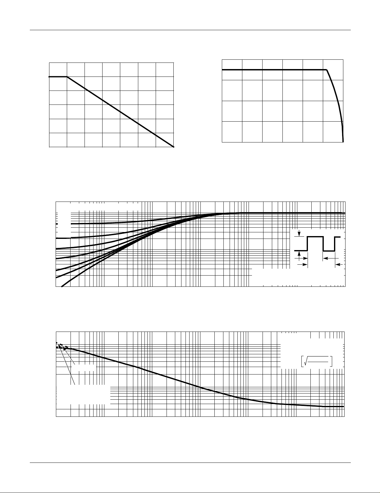
Typical Performance Curves
ISL9N2357D3ST
1.2
1.0
0.8
0.6
0.4
0.2
POWER DISSIPATION MULTIPLIER
0
0255075100 175
125
150
TC, CASE TEMPERATURE (oC)
FIGURE 1. NORMALIZED POWER DISSIPATION vs CASE
TEMPERATURE
2
DUTY CYCLE - DESCENDING ORDER
0.5
1
0.2
0.1
0.05
0.02
0.01
0.1
, NORMALIZED
θJC
Z
THERMAL IMPEDANCE
0.01
-5
10
-4
10
-3
10
t, RECTANGULAR PULSE DURATION (s)
40
30
20
, DRAIN CURRENT (A)
10
D
I
0
25 50 75 100 125 150 175
TC, CASE TEMPERATURE (oC)
FIGURE 2. MAXIMUM CONTINUOUS DRAIN CURRENT vs
CASE TEMPERATURE
P
DM
t
NOTES:
DUTY FACTOR: D = t
PEAK TJ = PDM x Z
-2
10
-1
10
θJC
10
1/t2
x R
0
θJC
+ T
1
t
2
C
1
10
FIGURE 3. NORMALIZED MAXIMUM TRANSIENT THERMAL IMPEDANCE
2000
1000
VGS = 10V
100
TRANSCONDUCTANCE
, PEAK CURRENT (A)
DM
I
MAY LIMIT CURRENT
IN THIS REGION
10
-5
10
-4
10
-3
10
-2
10
-1
10
t, PULSE WIDTH (s)
TC = 25oC
FOR TEMPERATURES
ABOVE 25
CURRENT AS FOLLOWS:
I = I
o
C DERATE PEAK
150 - T
25
0
10
125
C
10
FIGURE 4. PEAK CURRENT CAPABILITY
©2002 Fairchild Semiconductor Corporation ISL9N2357D3ST Rev. B1
1
Page 4

Typical Performance Curves (Continued)
ISL9N2357D3ST
80
PULSE DURATION = 80µs
DUTY CYCLE = 0.5% MAX
= 15V
V
DD
60
40
, DRAIN CURRENT (A)
20
D
I
0
23456
VGS, GATE TO SOURCE VOLTAGE (V)
TJ = 175oC
TJ = 25oC
TJ = -55oC
80
= 10V
V
GS
60
40
, DRAIN CURRENT (A)
20
D
I
0
0.511.52
VDS, DRAIN TO SOURCE VOLTAGE (V)
VGS = 7V
VGS = 6V
FIGURE 5. TRANSFER CHARACTERISTICS FIGURE 6. SATURATION CHARACTERISTICS
1.6
PULSE DURATION = 80µs
DUTY CYCLE = 0.5% MAX
1.4
1.2
1.0
ON RESIST ANCE
0.8
NORMALIZED DRAIN TO SOURCE
0.6
-80 -40 0 40 80 120 160 200
TJ, JUNCTION TEMPERATURE (oC)
VGS = 10V, ID = 20A
1.2
1.0
0.8
NORMALIZED GATE
0.6
THRESHOLD VOLTAGE
0.4
-80 -40 0 40 80 120 160 200
TJ, JUNCTION TEMPERATURE (oC)
VGS = 5V
TC = 25oC
PULSE DURATION = 80µs
DUTY CYCLE = 0.5% MAX
VGS = VDS, ID = 250µA
FIGURE 7. NORMALIZED DRAIN TO SOURCE ON
RESISTANCE vs JUNCTION TEMPERATURE
1.2
ID = 250µA
1.1
1.0
BREAKDOWN VOLTAGE
NORMALIZED DRAIN TO SOURCE
0.9
-80 -40 0 40 80 120 160 200
T
, JUNCTION TEMPERATURE (oC)
J
FIGURE 9. NORMALIZED DRAIN TO SOURCE BREAKDOWN
FIGURE 8. NORMALIZED GA TE THRESHOLD VOLTAGE vs
JUNCTION TEMPERATURE
10000
C
= CGS + C
ISS
C
≅ C
OSS
1000
C
RSS
C, CAPACITANCE (pF)
V
= 0V, f = 1MHz
100
GS
0.1 1 10
GD
+ C
DS
GD
= C
GD
VDS, DRAIN TO SOURCE VOLTAGE (V)
FIGURE 10. CAPACITANCE vs DRAIN TO SOURCE VOLTAGE
30
VOLTA GE vs JUNCTION TEMPERATURE
©2002 Fairchild Semiconductor Corporation ISL9N2357D3ST Rev. B1
Page 5

Typical Performance Curves (Continued)
10
VDD = 15V
8
6
ISL9N2357D3ST
, GATE TO SOURCE VOLTAGE (V)
GS
V
NOTE: Refer to Fairchild Application Notes AN7254 and AN7260.
FIGURE 11. GATE CHARGE WAVEFORMS FOR CONSTANT GATE CURRENT
Test Circuits and Waveforms
V
DS
V
GS
DUT
I
g(REF)
4
WAVEFORMS IN
DESCENDING ORDER:
2
0
0 20406080100
ID = 35A
I
= 20A
D
= 5A
I
D
Qg, GATE CHARGE (nC)
V
R
L
+
V
DD
-
DD
V
0
I
g(REF)
GS
V
GS
= 2V
V
DS
Q
g(10)
Q
g(TH)
Q
gs
Q
gd
0
Q
g(TOT)
VGS = 10V
V
= 20V
GS
FIGURE 12. GATE CHARGE TEST CIRCUIT FIGURE 13. GATE CHARGE WAVEFORMS
V
DS
R
L
V
GS
+
V
DD
-
V
DS
0
DUT
R
GS
V
GS
V
GS
10%
0
t
d(ON)
90%
t
ON
50%
t
10%
r
PULSE WIDTH
t
d(OFF)
90%
t
OFF
50%
t
f
90%
10%
FIGURE 14. SWITCHING TIME TEST CIRCUIT FIGURE 15. SWITCHING TIME WAVEFORM
©2002 Fairchild Semiconductor Corporation ISL9N2357D3ST Rev. B1
Page 6

PSPICE Electrical Model
.SUBCKT ISL9N2357 2 1 3 ; rev Aug 2000
CA 12 8 2.5e-9
CB 15 14 2.1e-9
CIN 6 8 5.2e-9
ISL9N2357D3ST
DBODY 7 5 DBODYMOD
DBREAK 5 11 DBREAKMOD
DPLCAP 10 5 DPLCAPMOD
EBREAK 11 7 17 18 33.39
EDS 14 8 5 8 1
EGS 13 8 6 8 1
ESG 6 10 6 8 1
EVTHRES 6 21 19 8 1
EVTEMP 20 6 18 22 1
IT 8 17 1
LDRAIN 2 5 1.0e-9
LGATE 1 9 4.3e-9
LSOURCE 3 7 1.6e-9
GATE
1
MMED 16 6 8 8 MMEDMOD
MSTRO 16 6 8 8 MSTROMOD
MWEAK 16 21 8 8 MWEAKMOD
RBREAK 17 18 RBREAKMOD 1
RDRAIN 50 16 RDRAINMOD 2.8e-3
RGATE 9 20 1.68
RLDRAIN 2 5 10
RLGATE 1 9 43
RLSOURCE 3 7 16
RSLC1 5 51 RSLCMOD 1e-6
RSLC2 5 50 1e3
RSOURCE 8 7 RSOURCEMOD 1.8e-3
RVTHRES 22 8 RVTHRESMOD 1
RVTEMP 18 19 RVTEMPMOD 1
S1A 6 12 13 8 S1AMOD
S1B 13 12 13 8 S1BMOD
S2A 6 15 14 13 S2AMOD
S2B 13 15 14 13 S2BMOD
VBAT 22 19 DC 1
LGATE
RLGATE
RGATE
9
CA
-
ESG
+
EVTEMP
+
-
18
22
20
S1A
12
13
8
S1B
EGS EDS
6
8
13
10
RSLC2
6
14
13
+
+
6
8
-
-
DPLCAP
EVTHRES
+
19
8
S2A
S2B
15
CB
CIN
-
+
-
5
51
5
51
21
MSTRO
14
5
8
RSLC1
+
ESLC
-
50
RDRAIN
16
8
MMED
DBREAK
EBREAK
MWEAK
RSOURCE
RBREAK
17 18
IT
8
RVTHRES
LDRAIN
RLDRAIN
11
+
17
18
DBODY
DRAIN
2
-
LSOURCE
7
RLSOURCE
RVTEMP
19
SOURCE
3
-
VBAT
+
22
ESLC 51 50 VALUE={(V(5,51)/ABS(V(5,51)))*(PWR( V(5,51)/(1e-6*550),3))}
.MODEL DBODYMOD D (IS = 1.01e-12 RS = 3.5e-3 ikf = 15 TRS1 = 1. 01e-3 TRS2 = 1.21e-6 CJO = 6.8 e-10 TT = 6.7e-9 M = 0.35)
.MODEL DBREAKMOD D (RS = 0.068 TRS1 = 1.12e-3 TRS2 = 1.25e-6)
.MODEL DPLCAPMOD D (CJO = 8.5e-10 I S = 1e-30 N = 10 M = 0.31)
.MODEL MMEDMOD NMOS (VTO = 3.5 KP = 6.0 IS = 1e-30 N = 10 TOX = 1 L = 1u W = 1u RG = 1.68)
.MODEL MSTROMOD NMOS (VTO = 4.1 KP = 110 IS = 1e-30 N = 10 TOX = 1 L = 1u W = 1u)
.MODEL MWEAKMOD NMOS (VTO = 3.0 KP = 0.03 IS = 1e-30 N = 10 TOX = 1 L = 1u W = 1u RG = 16.8 RS = 0.1)
.MODEL RBREAKMOD RES (TC1 = 1.01e-3 TC2 = 1.07e-7)
.MODEL RDRAINMOD RES (TC1 = 4.5e-3 TC2 = 8.0e-6)
.MODEL RSLCMOD RES (TC1 = 1.02e-4 TC2 = -1.13e-6)
.MODEL RSOURCEMOD RES (TC1 = 1.0e-3 TC2 = 1e-6)
.MODEL RVTHRESMOD RES (TC1 = -3.0e-3 TC2 = -1.5e-5)
.MODEL RVTEMPMOD RES (TC1 = -4.0e-3 TC2 = 1.25e-6)
.MODEL S1AMOD VSWITCH (RON = 1e-5 ROFF = 0.1 VON = -6.0 VOFF= -1.5)
.MODEL S1BMOD VSWITCH (RON = 1e-5 ROFF = 0.1 VON = -1.5 VOFF= -6.0)
.MODEL S2AMOD VSWITCH (RON = 1e-5 ROFF = 0.1 VON = -0.7 VOFF= 0)
.MODEL S2BMOD VSWITCH (RON = 1e-5 ROFF = 0.1 VON = 0 VOFF= -0.7)
.ENDS
NOTE: For further discussion of the PSPICE model, consult A New PSPICE Sub-Circuit for the Power MOSFET Featuring Globa l
Temperature Options; IEEE P ower Electronics Specialist Conference Records, 1991, written by William J. Hepp and C. Frank Wheatley.
©2002 Fairchild Semiconductor Corporation ISL9N2357D3ST Rev. B1
Page 7

ISL9N2357D3ST
SABER Electrical Model
REV Aug 2000
template ISL9N2357 n2,n1,n3
electrical n2,n1, n3
{
var i iscl
dp..model dbodym od = (isl = 1.01e-12, rs = 3.5e -3, ikf=15, trs1 = 1.01 e-3, trs2 = 1.21e-6, cjo = 6.8e-10, tt = 6.7e-9, m = 0.35)
dp..model dbreakmod = (rs = 0.068, trs1 = 1.12e-3, trs2 = 1.25e-6)
dp..model dplcapmod = (cjo = 8.5e-10, isl = 10e-30, nl=10, m = 0..31)
m..model mmedmod = (type=_n, vto = 3.5, kp = 6.0, is = 1e-30, tox = 1)
m..model mstrongmod = (type=_n, vto = 4.1, kp = 110, is = 1e-30, tox = 1)
m..model mweakmod = (type=_n, vto = 3.0, kp = 0.03, is = 1e-30, tox = 1, rs=0.1)
sw_vcsp..model s1amod = (ron = 1e-5, roff = 0.1, von = -6.0, voff = -1.5)
sw_vcsp..model s1bmod = (ron =1e-5, roff = 0.1, von = -1.5, voff = -6.0)
sw_vcsp..model s2amod = (ron = 1e-5, roff = 0.1, von = -0.7, voff = 0)
sw_vcsp..model s2bmod = (ron = 1e-5, roff = 0.1, von = 0, voff = -0.7)
c.ca n12 n8 = 2.5e-9
c.cb n15 n14 = 2.1e-9
c.cin n6 n8 = 5.5e-9
dp.dbody n7 n5 = model=dbodymod
dp.dbreak n5 n11 = model=dbreakmod
dp.dplcap n10 n5 = mo del=dplcapmod
i.it n8 n17 = 1
l.ldrain n2 n5 = 1.0e-9
l.lgate n1 n9 = 4.3e-9
l.lsource n3 n7 = 1.6e-9
GATE
LGATE
1
RLGATE
RGATE
9
m.mmed n16 n6 n8 n8 = model=mmedmod, l=1u, w=1u
m.mstrong n16 n6 n8 n8 = model=mstrongmod, l=1u, w=1u
m.mweak n16 n21 n8 n8 = model= mweakmod, l=1u, w=1u
res.rbreak n17 n18 = 1, tc1 = 1.01e-3, tc2 = 1.07e-7
res.rdrain n50 n16 = 2.8e-3, tc1 = 4.5e-3, tc2 = 8.0e-6
12
res.rgate n9 n20 = 1.6 8
res.rldrain n2 n5 = 10
res.rlgate n1 n9 = 43
res.rlsource n3 n7 = 16
res.rslc1 n5 n51= 1e-6, tc1 = 1.02e-4, tc2 = -1.13e-6
CA
res.rslc2 n5 n50 = 1e3
res.rsource n8 n7 = 1. 8e-3, tc1 = 1.0e-3, tc2 =1e-6
res.rvtemp n18 n19 = 1, tc1 = -4.0e-3, tc2 = 1.25e-6
res.rvthres n22 n8 = 1, tc1 = -3.0e-3, tc2 = -1 .5e-5
spe.ebreak n11 n7 n17 n18 = 33.39
spe.eds n14 n8 n5 n8 = 1
spe.egs n13 n8 n6 n8 = 1
spe.esg n6 n10 n6 n8 = 1
spe.evtemp n20 n6 n18 n22 = 1
spe.evthres n6 n21 n19 n8 = 1
sw_vcsp.s1a n6 n12 n13 n8 = model=s1amod
sw_vcsp.s1b n13 n12 n13 n8 = model=s1bmod
sw_vcsp.s2a n6 n15 n14 n13 = model=s2amod
sw_vcsp.s2b n13 n15 n14 n13 = model=s2bmod
v.vbat n22 n19 = dc=1
ESG
EVTEMP
+
18
22
20
S1A
13
S1B
EGS EDS
DPLCAP
10
RSLC2
-
6
8
EVTHRES
+
+
6
-
S2A
14
13
8
S2B
13
+
+
6
8
-
-
5
RSLC1
51
ISCL
MMED
DBREAK
11
MWEAK
EBREAK
RSOURCE
RBREAK
17 18
IT
8
RVTHRES
50
RDRAIN
16
21
-
19
8
MSTRO
CIN
15
CB
8
14
+
5
8
-
+
17
18
-
7
RLSOURCE
RVTEMP
19
-
+
22
LDRAIN
RLDRAIN
DBODY
LSOURCE
VBAT
DRAIN
2
SOURCE
3
equations {
i (n51->n50) +=iscl
iscl: v(n51,n50) = ((v(n 5,n51)/(1e-9+abs(v(n5,n51))))*((abs(v(n5, n51)*1e6/550))** 3))
}
}
©2002 Fairchild Semiconductor Corporation ISL9N2357D3ST Rev. B1
Page 8

SPICE Thermal Model
REV 23March 2000
ISL9N2357T
CTHERM1 th 6 3.0e-3
CTHERM2 6 5 4.0e-3
CTHERM3 5 4 4.8e-3
CTHERM4 4 3 5.2e-3
CTHERM5 3 2 8.5e-3
CTHERM6 2 tl 5.0e-2
RTHERM1 th 6 3.5e-3
RTHERM2 6 5 8.5e-3
RTHERM3 5 4 5.7e-2
RTHERM4 4 3 2.5e-1
RTHERM5 3 2 4.3e-1
RTHERM6 2 tl 4.5e-1
ISL9N2357D3ST
RTHERM1
RTHERM2
JUNCTION
th
CTHERM1
6
CTHERM2
5
SABER Thermal Model
SABER thermal model ISL9N2357T
template thermal_model th tl
thermal_c th, tl
{
ctherm.ctherm1 th 6 = 3.0e-3
ctherm.ctherm2 6 5 = 4.0e-3
ctherm.ctherm3 5 4 = 4.8e-3
ctherm.ctherm4 4 3 = 5.2e-3
ctherm.ctherm5 3 2 = 8.5e-3
ctherm.ctherm6 2 tl = 5.0e-2
rtherm.rtherm1 th 6 = 3.5e-3
rtherm.rtherm2 6 5 = 8.5e-3
rtherm.rtherm3 5 4 = 5.7e-2
rtherm.rtherm4 4 3 = 2.5e-1
rtherm.rtherm5 3 2 = 4.3e-1
rtherm.rtherm6 2 tl = 4.5e-1
}
RTHERM3
RTHERM4
RTHERM5
RTHERM6
CTHERM3
4
CTHERM4
3
CTHERM5
2
CTHERM6
CASE
tl
©2002 Fairchild Semiconductor Corporation ISL9N2357D3ST Rev. B1
Page 9

TRADEMARKS
The following are registered and unregistered trademarks Fairchild Semiconductor owns or is authorized to use and is
not intended to be an exhaustive list of all such trademarks.
ACEx
Bottomless
CoolFET
CROSSVOL T
DenseTrench
DOME
EcoSPARK
E2CMOS
EnSigna
TM
TM
FACT
FACT Quiet Series
STAR*POWER is used under license
FAST
FASTr
FRFET
GlobalOptoisolator
GTO
HiSeC
2
I
C
ISOPLANAR
LittleFET
MicroFET
MicroPak
MICROWIRE
OPTOLOGIC
â
OPTOPLANAR
PACMAN
POP
Power247
PowerTrench
â
QFET
QS
QT Optoelectronics
Quiet Series
SILENT SWITCHER
SMART START
SPM
STAR*POWER
Stealth
SuperSOT-3
SuperSOT-6
SuperSOT-8
SyncFET
TinyLogic
TruTranslation
ââ
UHC
UltraFET
VCX
DISCLAIMER
FAIRCHILD SEMICONDUCTOR RESERVES THE RIGHT TO MAKE CHANGES WITHOUT FURTHER
NOTICE TO ANY PRODUCTS HEREIN TO IMPROVE RELIABILITY, FUNCTION OR DESIGN. FAIRCHILD
DOES NOT ASSUME ANY LIABILITY ARISING OUT OF THE APPLICATION OR USE OF ANY PRODUCT
OR CIRCUIT DESCRIBED HEREIN; NEITHER DOES IT CONVEY ANY LICENSE UNDER ITS PATENT
RIGHTS, NOR THE RIGHTS OF OTHERS.
LIFE SUPPORT POLICY
â
FAIRCHILDS PRODUCTS ARE NOT AUTHORIZED FOR USE AS CRITICAL COMPONENTS IN LIFE SUPPORT
DEVICES OR SYSTEMS WITHOUT THE EXPRESS WRITTEN APPROVAL OF FAIRCHILD SEMICONDUCTOR CORPORATION.
As used herein:
1. Life support devices or systems are devices or
systems which, (a) are intended for surgical implant into
the body, or (b) support or sustain life, or (c) whose
failure to perform when properly used in accordance
with instructions for use provided in the labeling, can be
reasonably expected to result in significant injury to the
user.
PRODUCT STATUS DEFINITIONS
Definition of Terms
Datasheet Identification Product Status Definition
Advance Information
Preliminary
No Identification Needed
Formative or
In Design
First Production
Full Production
2. A critical component is any component of a life
support device or system whose failure to perform can
be reasonably expected to cause the failure of the life
support device or system, or to affect its safety or
effectiveness.
This datasheet contains the design specifications for
product development. Specifications may change in
any manner without notice.
This datasheet contains preliminary data, and
supplementary data will be published at a later date.
Fairchild Semiconductor reserves the right to make
changes at any time without notice in order to improve
design.
This datasheet contains final specifications. Fairchild
Semiconductor reserves the right to make changes at
any time without notice in order to improve design.
Obsolete
Not In Production
This datasheet contains specifications on a product
that has been discontinued by Fairchild semiconductor.
The datasheet is printed for reference information only.
Rev. H5
 Loading...