

®
www.BDTIC.com/Intersil
ISL97634
Data Sheet March 7, 2008
White LED Driver with Wide PWM
Dimming Range
The ISL97634 represents an efficient and highly integrated
PWM boost LED driver that is suitable for 1.8” to 3.5” LCDs
that employ 2 to 7 white LEDs for backligh ti n g. With
integrated Schottky diode, OVP, and wide range of PWM
dimming capability , the ISL97634 provides a simple, reliable,
and flexible solution to the backlight designers.
The ISL97634 features a wide range of PWM dimming
control capability. It allows dimming frequency as low as DC
to 32kHz beyond audible spectrum. The ISL97634 also
features a feedback disconnect switch to prevent the output
from being modulated by the PWM dimming signal that
minimizes system disturbance.
The ISL97634 is available in the 8 Ld TDFN (2mmx3mm)
package. There are 14V , 18V, and 26V OVP options that are
suitable for 3 LEDS, 4 LEDs, and 7 LEDs (3.5V/20mA type)
backlight applications respectively. The ISL97634 is
specified for operation over the -40°C to +85°C ambient
temperature at input voltage from 2.4V to 5.5V.
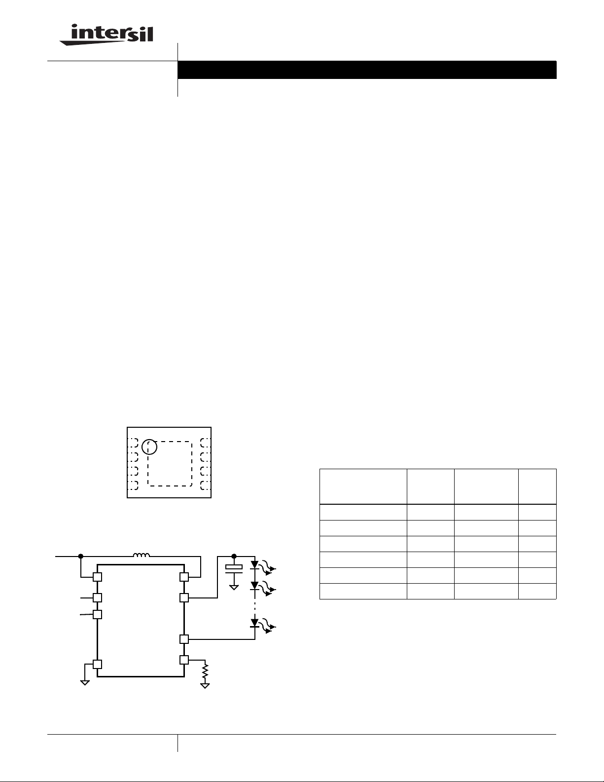
Pinout
ISL97634
(8 LD TDFN)
TOP VIEW
GND
VIN
PWM/EN
NC
1
2
3
4
8
7
6
5
LX
VOUT
FBSW
FB
Typical Application Circuit
VIN
PWM/EN
NC
GND
10µH or 22µH
LX
VOUT
FBSW
FB
VIN
FN6264.3
Features
• Drives Up to 7 LEDs in Series (3.5V/20mA type)
• OVP (14V , 18V, and 26V for 3, 4 and 7 LEDs Applications)
• PWM Dimming Control From DC to 32kHz
• Output Disconnect Switch
• Integrated Schottky Diode
• 2.4V to 5.5V Input
• 85% Efficiency
• 1.4MHz Switching Frequency Allows Small LC
• 1µA Shutdown Current
• Internally Compensated
• 8 Ld TDFN (2mmx3mm)
• Pb-Free (RoHS Compliant)
Applications
• LED Backlighting for:
- Cell phones
- Smartphones
-MP3
-PMP
- Automotive Navigation Panel
- Portable GPS
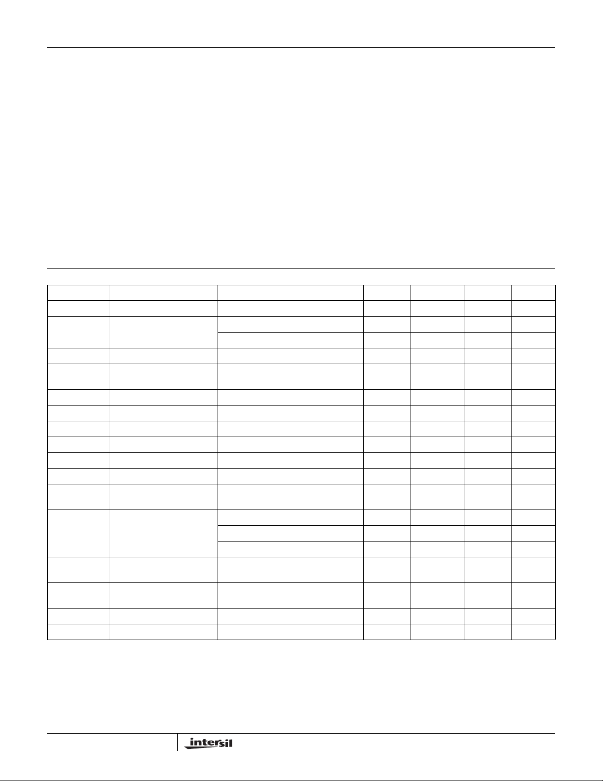
Ordering Information
PART
NUMBER
(Note)
ISL97634IRT14Z-T ELE 8 Ld 2x3 TDFN L8.2x3A
ISL97634IRT14Z-TK ELE 8 Ld 2x3 TDFN L8.2x3A
ISL97634IRT18Z-T ELF 8 Ld 2x3 TDFN L8.2x3A
ISL97634IRT18Z-TK ELF 8 Ld 2x3 TDFN L8.2x3A
ISL97634IRT26Z-T ELG 8 Ld 2x3 TDFN L8.2x3A
ISL97634IRT26Z-TK ELG 8 Ld 2x3 TDFN L8.2x3A
*Please refer to TB347 for details on reel specifications
NOTE: These Intersil Pb-free plastic packaged products employ
special Pb-free material sets; molding compounds/die attach
materials and 100% matte tin plate PLUS ANNEAL - e3 termination
finish, which is RoHS compliant and compatible with both SnPb and
Pb-free soldering operations. Intersil Pb-free products are MSL
classified at Pb-free peak reflow temperatures that meet or exceed
the Pb-free requirements of IPC/JEDEC J STD-020..
PART
MARKING
PACKAGE
(Pb-free)
Tape & Reel
PKG.
DWG.
#
1
CAUTION: These devices are sensitive to electrostatic discharge; follow proper IC Handling Procedures.
1-888-INTERSIL or 1-888-468-3774
| Intersil (and design) is a registered trademark of Intersil Americas Inc.
All other trademarks mentioned are the property of their respective owners.
Copyright Intersil Americas Inc. 2006-2008. All Rights Reserved
ISL97634
www.BDTIC.com/Intersil
Absolute Maximum Ratings (T
Input Voltage (V
LX Voltage . . . . . . . . . . . . . . . . . . . . . . . . . . . . . . . . . . .-0.3V to 28V
FBSW Voltage . . . . . . . . . . . . . . . . . . . . . . . . . . . . . . . .-0.3V to 28V
All Other Pins. . . . . . . . . . . . . . . . . . . . . . . . . . . . . . . . . .-0.3V to 6V
) . . . . . . . . . . . . . . . . . . . . . . . . . . . . .-0.3V to 6V
IN
Operating Conditions
Temperature Range . . . . . . . . . . . . . . . . . . . . . . . . . .-40°C to +85°C
CAUTION: Do not operate at or near the maximum ratings listed for extended periods of time. Exposure to such conditions may adversely impact product reliability and
result in failures not covered by warranty.
IMPORTANT NOTE: All parameters having Min/Max specifications are guaranteed over temperature of -40°C to +85°C unless otherwise stated. Typ values are for
information purposes only at TJ = TC = TA = +25°C.
NOTE:
1. θ
is measured in free air with the component mounted on a high effective thermal conductivity test board with “direct attach” features. See
JA
Tech Brief TB379.
2. For θ
, the “case temp” location is the center of the exposed metal pad on the package underside.
JC
Electrical Specifications V
PARAMETER DESCRIPTION CONDITION MIN TYP MAX UNIT
V
IN
I
IN
f
SW
DMAX Maximum Switching Duty
I
LIM
R
SW(LX)
ILEAK LX Switch Leakage Current VLX = 28V 0.01 1 µA
VFB Feedback Voltage 90 95 100 mV
IFB FB Pin Bias Current VFB = 95mV 1 µA
R
SW(FBSW)
V
DIODE
OVP Overvoltage Protection ISL97634IRT14Z 14 V
VIL Logic Low Voltage of
VIH Logic High Voltage of
PWM_on Minimum PWM On-Time 1.5 µs
EN_delay EN to Vout Delay 200 µs
Supply Voltage 2.4 5.5 V
Supply Current PWM/EN = 3V, enabled, not switching 0.8 1.5 mA
Switching Frequency 1,300 1,450 1,600 kHz
Cycle
LX Current 400 470 mA
LX Switch ON-Resistance ILX = 100mA 900 mΩ
FBSW Switch ON-Resistance 10 Ω
Schottky Diode Forward
Voltage
PWM/EN
PWM/EN
= +25°C) Thermal Information
A
Thermal Resistance θ
8 Ld TDFN Package (Notes 1, 2). . . . . 77 12
Maximum Junction Temperature . . . . . . . . . . . . . . . . . . . . . .+125°C
Storage Temperature . . . . . . . . . . . . . . . . . . . . . . .-65°C to +150°C
Pb-free reflow profile . . . . . . . . . . . . . . . . . . . . . . . . . .see link below
http://www.intersil.com/pbfree/Pb-FreeReflow.asp
= V
IN
= 3V
PWM/EN
PWM/EN = 0V, disabled 1 µA
IDIODE = 100mA, TA = +25°C 600 850 mV
ISL97634IRT18Z 18 V
ISL97634IRT26Z 26 28 V
(°C/W) θ
JA
90 95 %
0.6 V
1.5 V
JC
(°C/W)
2
FN6264.3
March 7, 2008
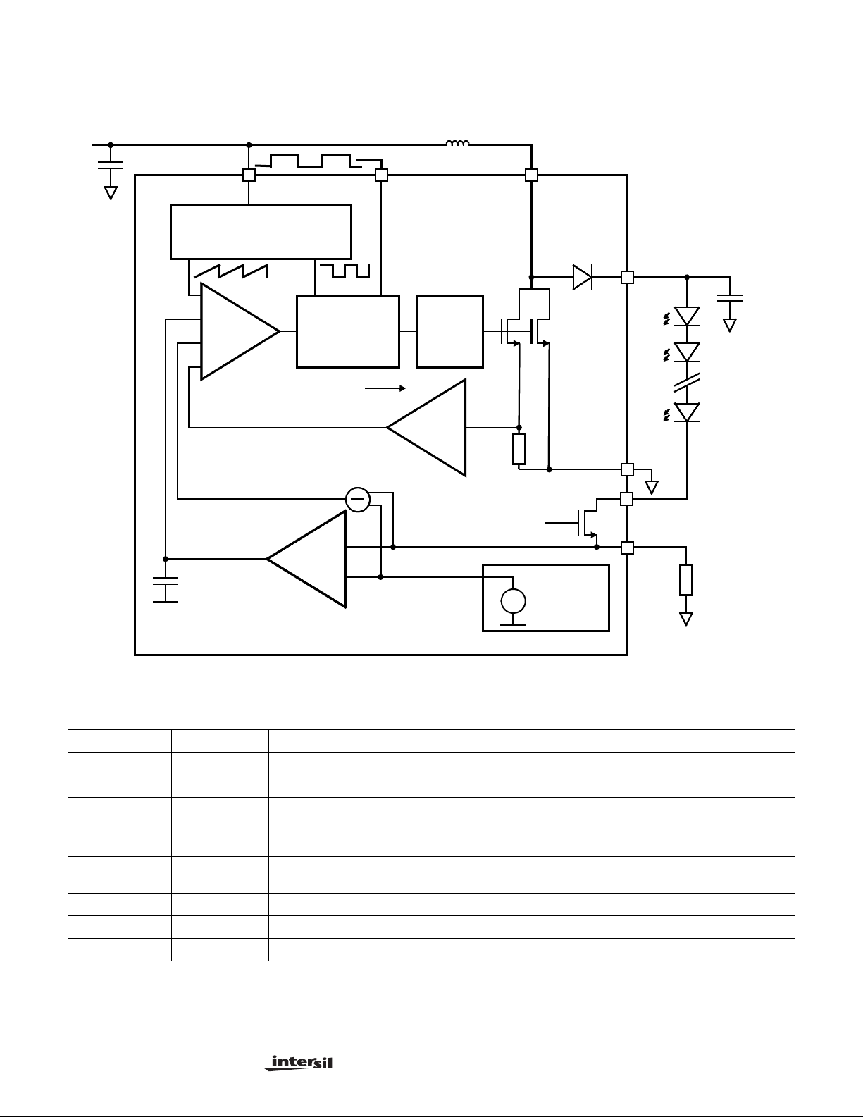
Block Diagram
www.BDTIC.com/Intersil
VIN (2.4V TO 5.5V)
CIN
ISL97634
L
VIN PWM/EN LX
1.4MHZ OSCILLATOR AND RAMP
GENERATOR
PWM
COMPARATOR
GM AMP
GM AMP
COMPENSATION
COMPENSATION
CONTROLLER
GM
AMPLIFIER
ISL97634
DRIVER
CURRENT
SENSE
95mV
VOUT
COUT
FET PWM LOGIC
2 LEDs to 7 LEDS
GND
FBSW
PWM/EN
FB
BANDGAP
REFERENCE
GENERATOR
RSET
Pin Description
PIN NUMBER PIN NAME DESCRIPTION
1 GND Ground Pin. Conn ect to local grou nd.
2 VIN In put Supply Pin. Connect to the input supply voltage, the inductor and the input supply de coupling capacitor .
3 PWM/EN PWM or Enable Pin. Connect external PWM signal allows pulse width modulation current operation. Enable
signal allows peak current operation or disable signal shuts dow n th e de vice.
4 NC No Connect
5 FB Feedback Pin. Connect the sense resistor between FB and ground. The cathode of bot tom LED ca n also
be connected at this pin if the output current is not to b e P WMed.
6 FBSW FB Disconnect Switch. Connect to the cathode of the bottom LED if the output current to be PWMed.
7 VOUT Output Pin. Connect to the anode of the top LED and the output filter capacitor.
8 LX Switching Pin. Connect to inductor.
3
FN6264.3
March 7, 2008

Typical Performance Curves
www.BDTIC.com/Intersil
ISL97634
90
85
80
75
70
65
EFFICIENCY (%)
60
55
50
7 LEDs, 22µH
0 20406080100
3 LEDs, 10µH
3 LEDs, 22µH
PWM DUTY CYCLE (%)
4 LEDs, 10µH
7 LEDs, 10µH
ILED_peak = 25mA
VIN = 4V
RSET = 4Ω
= 1kHz
f
PWM
1.0
0.8
0.6
0.4
(mA)
q
I
0.2
0.0
-0.2
0246
135
V
(V)
IN
FIGURE 1. EFFICIENCY vs PWM DUTY CYCLE FIGURE 2. QUIESCENT CURRENT vs VIN (PWM/EN = HI)
(mA)
O
I
20.08
20.04
20.00
19.76
19.74
19.72
19.70
(mA)
O
I
19.68
19.96
19.92
0 5 10 15 20 25 30
FIGURE 3. LOAD REGULATION (V
100
7 LEDs
90
V
= 4V
IN
80
RSET = 4Ω
L = 10µH
70
60
50
40
FB VOLTAGE (mV)
30
20
10
0
0 20 40 60 80 100 120
V
(V)
OUT
1kHz
20kHz
32kHz
DUTY CYCLE (%)
= 4V) FIGURE 4. LINE REGULATION
IN
19.66
19.64
19.62
2.5 3.0 3.5 4.0 4.5 5.0 5.5
V
(V)
IN
V
OUT
LX
PWM/EN
ILED
VIN = 4V
R
L
= 4Ω
1
= 22µH
1
FIGURE 5. DIMMNG LINEARITY (FB VOLT AGE) vs DUTY
FIGURE 6. PWM DIMMING AT 1kHz, D = 1%
CYCLE
4
FN6264.3
March 7, 2008

V
www.BDTIC.com/Intersil
OUT
LX
ISL97634
V
OUT
LX
PWM/EN
VIN = 4V
= 4
Ω
R
1
ILED
FIGURE 7. PWM DIMMING AT 1kHz, D = 1% ZOOM IN FIGURE 8. PWM DIMMING AT 1kHz, D = 99%
L1 = 22µH
V
R1 = 4
Ω
VIN = 4V
L1 = 22µH
PWM/EN
OUT
LX
ILED
PWM/EN
ILED
VIN = 4V
= 4
Ω
R
1
L1 = 22µH
FIGURE 9. PWM DIMMING AT 20kHz, D = 50%
Detailed Description
The ISL97634 uses a constant frequency, current mode
control scheme to provide excellent line and load
regula tion. There are three OVP models for driving 3, 4
and 7 LEDs (3.5V/20mA type) and their OVP thresholds
are set at 14V, 18V and 26V respectively. The ISL97634
operates from an input voltage of 2.4V to 5.5V and ambient
temperature from -40°C to +85°C. The switching frequency
is around 1.45MHz and allows the driver circuit to employ
small LC components. The peak forward current of the LED
is set using the R
LED peak current is given by Equation1:
V
FB
---------------
=
I
LED
R
SET
PWM Dimming
The ISL97634’s PWM/EN pin can be tied permanently to
high for a fixed current operation. On the other hand, the
ISL97634 can be applied with an external PWM signal to
resistor. In the steady state mode, the
SET
5
(EQ. 1)
pulse width modulated output current. It is well understood
that the LED brightness is a linear function of the LED
current. In addition, the average LED current corresponds to
the duty cycle “D” of the PWM signal as shown in
Equation 2:
V
FB
I
LED-AVG
---------------
R
SET
D⋅=
(EQ. 2)
As a result, PWM signal provides a means to dim the LED
brightness. PWM dimming offers the best LEDs matching
over DC dimming. It is because the LED peak current
operating point is far away from the knee of the diode I-V
curve where part to part variations are high. The PWM
dimming test results are shown in Figure 6 with two PWM
frequencies, 1kHz and 20kHz. The vertical scale parameter
FB is proportional to the current and therefore the
brightness.
For the ISL97634, PWM dimming provides linear dimming
adjustment with low frequency signal, such as 1kHz and
FN6264.3
March 7, 2008

ISL97634
www.BDTIC.com/Intersil
below. The applied PWM dimming signal can be up to
32kHz; however, the dimming linearity is compromised at
low duty cycles as their durations are too short for the
ISL97634’s control loop to respond properly. This
non-ideality behavior does not cause any functional
problem. The PWM dimming linear responses in Figure 5
are expanded in Figure 10. At 1kHz PWM dimming, the duty
cycle can virtually vary from below 1% to DC. On the other
hand, at 20kHz PWM dimming, the linearity range is from
5% to DC only.
10
7 LEDs
9
V
= 4V
IN
RSET = 4Ω
8
L = 10µH
7
6
5
4
FB VOLTAGE (mV)
3
2
1
0
024681012
FIGURE 10. DIMMING LINEARITY vs DUTY CYCLES ZOOM IN
1kHz
20kHz
32kHz
DUTY CYCLE (%)
The low level non-linearity effects at high frequency PWM
dimming is also reflected in the efficiency measurements in
Figure 11.
90
85
80
75
70
65
EFFICIENCY (%)
60
55
50
0 5 10 15 20 25 30
FIGURE 11. EFFICIENCY vs PWM DIMMING FREQUENCIES
ILED (mA)
3 LEDs
V
= 4V
IN
RSET = 4
L = 22µH
Ω
Feedback Disconnect Switch
The ISL97634 functions properly without using the FBSW.
However, the output cap a citor will disch arge during the PWM
off time resulting in poor dimming linearity at low duty cycles.
The output discharge effect can be seen in Figure 12.
Moreover, the output is modulated by the PWM signal that
may create interference to other systems.
.
V
OUT
LX
PWM/EN
VIN = 4V
ILED
FIGURE 12. PWM DIMMING AT 1kHz WITHOUT USING FBSW
R1 = 4Ω
L1 = 22µH
The FBSW should be used for PWM dimming as illustrated
in “Typical Application Circuit” on page 1. During the PWM
off time, the FBSW is opened. The LEDs are floating and
therefore the output capacitor has no path to discharge. The
LED current responds accurately with the PWM signal (see
Figure 13). The output switches very quickly to the target
current with minimal settling ringing and without being
modulated by the PWM signal, and therefore minimizes any
system disturbance.
V
OUT
LX
PWM/EN
ILED
FIGURE 13. PWM DIMMING AT 1kHz USING FBSW
VIN = 4V
Ω
R1 = 4
L1 = 22µH
Overvoltage Protection
The ISL97634 comes with overvoltage protection. The OVP
trip points are at 14V, 18V and 26V for ISL97634IRT14Z,
ISL97634IRT18Z and ISL97634IRT26Z respectively. The
maximum numbers of LEDs and OVP threshold are shown in
Table 1. When the device reaches the OVP, the LX stops
switching, disabling the boost circuit until V
below the OVP threshold. At this point, LX will be allowed to
switch again. The OVP event will not cause the device to
shutdown.
There are three OVP options so that the 3 LEDs application
should use the 14V OVP device and the 7 LEDs application
should use the 26V OVP device. An output capacitor that is
falls about 7%
OUT
6
FN6264.3
March 7, 2008

ISL97634
www.BDTIC.com/Intersil
only rated for the required voltage range can therefore be
used, which will optimize the component costs in so me cases.
TABLE 1.
PART NO. OVP
ISL97634IRT14Z 14V 3 70mA
ISL97634IRT18Z 18V 4 50mA
ISL97634IRT26Z 26V 7 30mA
MAX NO. OF
LEDS MAX ILED
Shutdown
When PWM/EN is taken low the ISL97634 enters into the
power-down mode where the supply current is reduced to
less than 1µA. The device resumes normal when the
PWM/EN goes high.
Components Selection
The input capacitance is typically 0.22µF. The output
capacitor should be in the range of 0.22µF to 1µF. X5R or
X7R type of ceramic capacitors of the appropriate voltage
rating are recommended.
When choosing an inductor, make sure the average and
peak current ratings are adequate by using Equations 3, 4 and
5 (80% efficiency assumed):
I
⋅
LEDVOUT
I
LAVG
I
LPKILAVG
---------------------------------
=
0.8 V
⋅
IN
1
-- -
Δ⋅+=
I
L
2
(EQ. 3)
(EQ. 4)
Compensation
The product of the output capacitor and the load create a
pole while the inductor creates a right half plane zero. Both
of these attributes degrade the phase margin but the
ISL97634 has internal compensation network that ensures
the device operates reliably under the specified conditions.
The internal compensation and the highly integrated
functions of the ISL97634 make it a design friendly device to
be used in high volume, high reliability applications.
Applications
Analog Dimming
Analog dimming is usually not recommended because of the
brightness non-linearity at low levels dimming. However,
some systems are EMI or noise sensitive that analog
dimming may be more suitable than PWM dimming under
those situations. The ISL97632 is part of the same family as
the ISL97634 and has been designed with a serial interface
to give access to 32 separate dimming levels. Alternatively
analog dimming can be achieved by applying a variable DC
voltage (V
current. As the DC dimming signal voltage increases above
VFB, the voltages drop on R
voltage drop on RSET decreases. Thus, the LED current
decreases as shown in Equation 6:
=
I
LED
If V
DIM
brightness will increase.
) at FB pin (see Figure 14) to adjust the LED
Dim
and R2 increase and the
1
VFBR1R2+()V
------------------------------------------------------------------------- -
R⋅
R
2
SET
⋅–⋅
DimR1
(EQ. 6)
is taken below FB, the inverse will happen and the
V
INVOUTVIN
---------------------------------------------------
Δ
I
=
L
LV
⋅⋅
–()⋅
OUTfOSC
(EQ. 5)
Where:
• ΔI
is the peak-to-peak inductor current ripple in Amps
L
• L is the inductance in H
is the switching frequency, typically 1.45MHz
•f
OSC
The ISL97634 supports a wide range of inductance values
(10µH to ~82µH). For lower inductor values or lighter loads,
the boost inductor current may become discontinuous. For
high boost inductor values, the boost inductor current will be
in continuous mode.
In addition to the inductor value and switching frequency, the
input voltage, number of LEDs and the LED current also
affects whether the converter operates in continuous
conduction or discontinuous conduction mode.
Both operating modes are allowed and normal. The
discontinuous conduction mode yields lower efficiency due
to higher peak current.
The DC dimming signal voltage can be a variable DC voltage
from a POT, a DCP (Digitally Controlled Potentiometer), or a
DC voltage generated by filtering a high frequency PWM
control signal.
L1
22µH
V
IN
3.3V
C1
1µF
FIGURE 14. ANALOG DIMMING CONTROL APPLICATION
CIRCUIT
V
LX
LX
IN
V
OUT
ISL97634
PWM FB
GND
R2
As brightness is directly proportional to LED currents, V
R1
3.3k
LEDs
C2
0.22µF
R
SET
4.75Ω
V
Dim
Dim
may be calculated for any desired “relative brightness” (F)
using Equation 7:
R
2
Dim
-------
R
1
V
Where F = I
⋅⋅=
V
LED
FB
R
⎛⎞
1
-------
1
⎜⎟
⎝⎠
(dimmed)/I
F–+
R
2
(undimmed).
LED
(EQ. 7)
7
FN6264.3
March 7, 2008

ISL97634
www.BDTIC.com/Intersil
These equations are valid for values of R1 and R2 such that
both R
>>RSET and R2>>RSET.
1
The analog dimming circuit can be tailored to a desired
relative brightness for different V
ranges using
Dim
Equation 8.
V
Dim_maxVFB
-------------------------------------------------------------------
R
=
2
Where V
V
Dim_max
–()R1•[]
1F
–()•[]
FB
min
is the maximum V
voltage and F
Dim
(EQ. 8)
min
the minimum relative brightness (i.e., the brightness with
V
Dim_max
i.e., V
i.e., V
applied).
Dim_max
Dim_max
= 5V, F
= 1V, F
= 10% (i.e., 0.1), R2 = 189k
min
= 10% (i.e., 0.1), R2 = 35k
min
Efficiency Improvement
Figure 1 shows the efficiency measurement s during PWM
operation. The choice of the inductor has a significant impact
on the power efficiency. As shown in Equation 4, the higher
the inductance, the lower the peak current, therefore, the
lower the conduction and switching losses. On the other hand,
it has also a higher series resistance. Neverthe less, the
efficiency improvement effect by lowering the peak current is
greater than the resistance increases with larger value of
inductor. Effi ciency can also be improved for systems that
have high supply voltages. Since the ISL97634 can only
supply from 2.4V to 5.5V, V
high supply voltage for the boost circuit as shown in Figure 15
and the efficiency improvement is shown in Figure 16.
Vs = 12V
C1
1µF
VIN = 2.7V TO 5.5V
0.1µF
C2
FIGURE 15. SEPARATE HIGH INPUT VOLT AGE FOR HIGHER
L1
1 2
22µH
VIN
ISL97634
PWM/EN
EFFICIENCY OPERATION
must be separated from the
IN
LX
VOUT
FBSW
FB
GND
C3
0.22µF
R1
D1
D2
D3
D4
D5
D6
4Ω
is
.
90
85
80
EFFICIENCY (%)
75
70
0 5 10 15 20 25 30
FIGURE 16. EFFICIENCY IMPROVEMENT WITH 9 AND 12V
VS = 12V
INPUTS
ILED (mA)
VS = 9V
VIN = 4V
7 LEDs
L1 = 22µH
R1 = 4Ω
f
PWM
8 LEDs Operation
For medium size LCDs that need more than 7 low power LEDs
for backlighting, such as a portable media player or automotive
navigation panel displays, the voltage range of the ISL97634 is
not sufficient. However, the ISL97634 can be used as an LED
controller with an external protection MOSFET connected in
cascode fashion to achieve higher output voltage. A conceptual
8 LEDs driver circuit is shown in Figure 17. A 60V logic level NChannel MOSFET is configured such that its drain ties between
the inductor and the anode of Schottky diode, its gate ties to the
input, and its source ties to the ISL97634 LX node connecting
to the drain of the internal switch. When the internal switch
turns on, it pulls the source of M1 down to ground and LX
conducts as normal. When the internal switch turns off, the
source of M1 will be pulled up by the follower action of M1,
limiting the maximum voltage on the ISL97634 LX pin to below
V
, but allowing the output voltage to go much higher than the
IN
breakdown limit on the LX pin. The switch current limit and
maximum duty cycle will not be changed by this setup, so input
voltage will need to be carefully considered to make sure that
the required output voltage and current levels are achievable.
Because the source of M1 is effectively floating when the
internal LX switch is off, the drain-to-source capacitance of M1
may be sufficient to capacitively pull the node high enough to
break down the gate oxide of M1. To prevent this, V
be connected to V
, allowing the internal Schottky diode to
IN
limit the peak voltage. This will also hold the VOUT pin at a
known low voltage, preventing the built in OVP function from
causing problems. This OVP function is effectively useless in
this mode as the real output voltage is outside its intended
range. If the user wants to implement their own OVP protection
(to prevent damage to the output capacitor), they should insert
a zener diode from VOUT to the FB pin. In this setup, it would
be wise not to use the FBSW to FB switch, as otherwise, the
zener diode will have to be a high power one capable of
dissipating the entire LED load power. Then the LED stack can
then be connected directly to the sense resistor via a 10kΩ
resistor to FB. A zener can be placed from VOUT to the FB pin
allowing an overvoltage event to pull-up on FB with a low
breakdown current (and thus low power zener diode) as a
result of the 10kΩ resistor.
OUT
should
8
FN6264.3
March 7, 2008

ISL97634
www.BDTIC.com/Intersil
V
= 2.7V TO 5.5V
IN
C1
1µF
C2
0.1µF
FIGURE 17. CONCEPTUAL 8 LEDs HIGH VOLTAGE DRIVER
L1
12
2.2µ
VOUT
VIN
PWM/EN
ISL97634
FBSW
GND
LX
FB
M1
R1
D0
10BQ100
FQT13N06L
SK011C226KAR
6.3Ω
C3
4.7µF
D1
D2
D3
D4
D5
D6
D7
D8
SEPIC Operation
For applications where the output voltage is not always
above the input voltage, a buck or boost regulation is
needed. A SEPIC (Single Ended Primary Inductance
Converter) topology, shown in Figure 18, can be considered
for such an application. A single cell Li-ion battery operating
a cellular phone backlight or flashlight is one example. The
battery voltage is between 2.5V and 4.2V, depending on the
state of charge. On the other hand, the output may require
only one 3V to 4V medium power LED for illumination
because the light guard of the backlight assembly is
optimized for cost efficiency trade-off reason.
In fact, a SEPIC configured LED driver is flexible enough to
allow the output to be well above or below the input voltage,
unlike the previous example. Another example is when the
number of LEDs and input requirements are different from
platform to platform, a common circuit and PCB that fit all the
platforms in some cases may be beneficial enough that it
outweighs the disadvantage of adding additional component
cost. L
The simplest way to understand SEPIC topology is to think
about it as a boost regulator where the input voltage is level
shifted downward at the same magnitude and the lowest
reference level starts at -V
and L2 can be a coupled inductor in one p ackage.
1
VIN = 2.7V TO 5.5V
C1
1µF
C2
0.1µF
L1
1
2
22µH
VOUT
ISL97634
FBSW
LX
FB
GND
VIN
SDIN
FIGURE 18. SEPIC LED DRIVER
IN
C3
V
A
1µF
R1
rather than 0V.
V
1Ω
B
D0
L2
22µH
C4 0.22µF
D1
The SEPIC works as follows; assume the circuit in Figure 18
operates normally when the ISL97634 internal switch opens
and it is in the PWM off state. After a short duration where few
LC time constants elapsed, the circuit is considere d in the
steady-state within the PWM off period that L
shorted. V
charged to V
is therefore shorted to the ground and C3 is
B
with VA = VIN. When the ISL97634 internal
IN
switch closes and the circuit is in the PWM on-state, V
pulled to ground. Since the voltage in C
instantaneously, V
is shifted downward and becomes -VIN.
B
The next cycle when the ISL97634 switch opens, V
and L2 are
1
is now
cannot be changed
3
A
boosts
B
up to the targeted output like the standard boost regulator
operation, except the lowest reference point is at -V
. The
IN
output is approximated in Equation 9:
=
------------------
1D–()
(EQ. 9)
V
OUTVIN
D
where D is the on-time of the PWM duty cycle.
The convenience of SEPIC comes with some trade-off in
addition to the additional L and C costs. The effi cie ncy is
usually lowered because of the relatively large efficien cy loss
through the Schottky diode if the output voltage is low. The L
series resistance also contributes additional loss. Figure 19
shows the efficiency measurement of a single LED application
as the input varies between 2.7V and 4.2V.
Note V
is considered the level-shifted LX node of a standard
B
boost regulator. The higher the input volt age, the lower the V
voltage will be during PWM on period. The result is that the
efficiency will be lower at higher input voltages be cause the
SEPIC has to work harder to boost up to the required level.
This behavior is the opposite to the standard boost regulator’s
and the comparison is shown in Figure 19.
76
72
68
EFFICIENCY (%)
64
60
0
FIGURE 19. EFFICIENCY MEASUREMENT OF A SINGLE LED
VIN = 2.7V
VIN = 4.2V
1 LED
L
= L2 = 22µH
1
C
= 1µF
3
= 4.7Ω
R
1
5101520
SEPIC DRIVER
ILED (mA)
PCB Layout Considerations
The layout is very import ant for the converter to function
properly. R
and GND pins. Longer traces to the LEDs are acceptable.
Similarly, the supply decoupling cap and the output filter cap
should be as close as possible to the VIN and VOUT pins.
The heat of the IC is mainly dissipated through the thermal pad
of the package. Maximizing the copper area connected to this
pad if possible. In addition, a solid ground plane is always
helpful for the EMI performance.
must be located as close as possible to the FB
SET
2
B
9
FN6264.3
March 7, 2008

ISL97634
www.BDTIC.com/Intersil
Thin Dual Flat No-Lead Plastic Package (TDFN)
(DATUM A)
NX (b)
5
INDEX
AREA
SEATING
(DATUM B)
6
INDEX
AREA
NX L
8
A
6
C
PLANE
(A1)
D
TOP VIEW
SIDE VIEW
D2
D2/2
12
N
N-1
e
(Nd-1)Xe
REF.
BOTTOM VIEW
2X
A3
NX b
L8.2x3A
ABC0.15
2X
0.15
CB
E
//
A
87
NX k
E2
E2/2
5
0.10
C
L
0.10
0.08
L
C
C
BAMC
8 LEAD THIN DUAL FLAT NO-LEAD PLASTIC PACKAGE
MILLIMETERS
SYMBOL
NOTESMIN NOMINAL MAX
A 0.70 0.75 0.80 A1 - - 0.05 A3 0.20 REF -
b 0.20 0.25 0.32 5,8
D 2.00 BSC -
D2 1.50 1.65 1.75 7,8
E 3.00 BSC E2 1.65 1.80 1.90 7,8
e 0.50 BSC -
k0.20 - - L 0.30 0.40 0.50 8
N 8 2
Nd 4 3
Rev. 0 6/04
NOTES:
1. Dimensioning and tolerancing conform to ASME Y14.5-1994.
2. N is the number of terminals.
3. Nd refers to the number of terminals on D.
4. All dimensions are in millimeters. Angles are in degrees.
5. Dimension b applies to the metallized terminal and is measured
between 0.25mm and 0.30mm from the terminal tip.
6. The configuration of the pin #1 identifier is optional, but must be
located within the zone indicated. The pin #1 identifier may be
either a mold or mark feature.
7. Dimensions D2 and E2 are for the exposed p ads which provide
improved electrical and thermal performance.
8. Nominal dimensions are provided to assist with PCB Land
Pattern Design efforts, see Intersil Technical Brief TB389.
SECTION "C-C"
FOR EVEN TERMINAL/SIDE
CC
e
TERMINAL TIP
All Intersil U.S. products are manufactured, assembled and tested utilizing ISO9000 quality systems.
Intersil Corporation’s quality certifications can be viewed at www.intersil.com/design/quality
Intersil products are sold by description only. Intersil Corporation reserves the right to make changes in circuit design, software and/or specifications at any time without
notice. Accordingly, the reader is cautioned to verify that data sheets are current before placing orders. Information furnished by Intersil is believed to be accurate and
reliable. However, no responsibility is assumed by Intersil or its subsidiaries for its use; nor for any infringements of patents or other rights of third parties which may result
from its use. No license is granted by implic atio n or other wise u nde r any p a tent or patent rights of Intersil or its subsidiaries.
For information regarding Intersil Corporation and its products, see www.intersil.com
10
FN6264.3
March 7, 2008
 Loading...