

Datasheet ISL95870AHRUZ, ISL95870AIRUZ, ISL95870BHRZ, ISL95870BIRZ, ISL95870HRUZ Datasheet (Intersil) [ru]
...Page 1
PWM DC/DC Controller with VID Inputs for Portable
RTN
GND
SREF
EN
C
BOOT
L
O
C
SEN
R
OCSET
Q
HS
Q
LS
3.3V TO 25V
0.5V TO 5V
R
O
CO
CIN
V
IN
V
OUT
C
SOFT
C
VCC
C
PVCC
GPIO
8
7
6
5
13
14
15
16
VO
OCSET
FB
FSEL
VCC
PVCC
LGATE
PGND
11
UGATE
BOOT
2
1
12
9
PGOOD
PHASE
4
3
10
+5V
R
VCC
R
PGOOD
RTN1
R
FB
R
OFS
R
OFS1
R
FB1
RTN1
0
GPU Core-Voltage Regulator
ISL95870, ISL95870A, ISL95870B
The ISL95870, ISL95870A, ISL95870B ICs are Single-Phase
Synchronous-Buck PWM regulators featuring Intersil’s
proprietary R
4
Technology™. The wide 3.3V to 25V input
voltage range is ideal for systems that run on battery or
AC-adapter power sources. The ISL95870A and ISL95870B
are low-cost solutions for applications requiring dynamically
selected slew-rate controlled output voltages. The soft-start
and dynamic setpoint slew-rates are capacitor programmed.
Voltage identification logic-inputs select four (ISL95870A,
ISL95870B) resistor-programmed setpoint reference voltages
that directly set the output voltage of the converter between
0.5V and 1.5V, and up to 5V with a feedback voltage divider.
3
Compared with R
modulator, the R4 modulator has
equivalent light-load efficiency, faster transient performance,
accurately regulated frequency control and all internal
compensation. These updates, together with integrated
MOSFET drivers and schottky bootstrap diode, allow for a
high-performance regulator that is highly compact and needs
few external components. The differential remote sensing for
output voltage and selectable switching frequency are another
two new functions. For maximum efficiency, the converter
automatically enters diode-emulation mode (DEM) during
light-load conditions such as system standby.
Features
• Input Voltage Range: 3.3V to 25V
• Output Voltage Range: 0.5V to 5V
• Precision Regulation
-Proprietary R
- ±0.5% System Accuracy Over -10°C to +100°C
• Optimal Transient Response
- Intersil’s R
•Output Remote Sense
• Extremely Flexible Output Voltage Programmability
- 2-Bit VID Selects Four Independent Setpoint Voltages for
ISL95870B
- 2-Bit VID Selects Four Dependent or Three Independent
Setpoint Voltages for ISL95870A
- Simple Resistor Programming of Setpoint Voltages
• Selectable 300kHz, 500kHz, 600kHz or 1MHz PWM
Frequency in Continuous Conduction
• Automatic Diode Emulation Mode for Highest Efficiency
• Power-Good Monitor for Soft-Start and Fault Detection
4
™ Frequency Control Loop
4
™ Modulator Technology
December 2, 2013
FN6899.1
Applications
• Mobile PC Graphical Processing Unit VCC Rail
• Mobile PC I/O Controller Hub (ICH) VCC Rail
• Mobile PC Memory Controller Hub (GMCH) VCC Rail
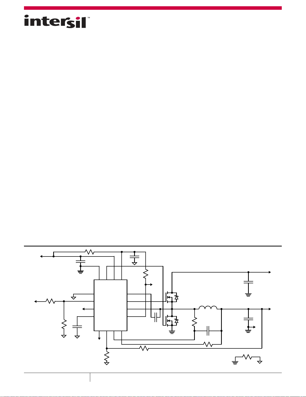
FIGURE 1. ISL95870 APPLICATION SCHEMATIC WITH ONE OUTPUT VOLTAGE SETPOINT AND DCR CURRENT SENSE
1
CAUTION: These devices are sensitive to electrostatic discharge; follow proper IC Handling Procedures.
1-888-INTERSIL or 1-888-468-3774
Intersil (and design) and R3 Technology are trademarks owned by Intersil Corporation or one of its subsidiaries.
| Copyright Intersil Americas LLC 2009, 2013. All Rights Reserved
All other trademarks mentioned are the property of their respective owners.
Page 2

ISL95870, ISL95870A, ISL95870B
Table of Contents
Applications Schematics: ISL95870 . . . . . . . . . . . . . . . . . . . . . . . . . . . . . . . . . . . . . . . . . . . . . . . . . . . . . . . . . . . . . . . . . . . . . . . . . . . . 3
Applications Schematics: ISL95870A. . . . . . . . . . . . . . . . . . . . . . . . . . . . . . . . . . . . . . . . . . . . . . . . . . . . . . . . . . . . . . . . . . . . . . . . . . . 4
Applications Schematics: ISL95870B. . . . . . . . . . . . . . . . . . . . . . . . . . . . . . . . . . . . . . . . . . . . . . . . . . . . . . . . . . . . . . . . . . . . . . . . . . . 5
Block Diagram . . . . . . . . . . . . . . . . . . . . . . . . . . . . . . . . . . . . . . . . . . . . . . . . . . . . . . . . . . . . . . . . . . . . . . . . . . . . . . . . . . . . . . . . . . . . . . 6
ISL95870 Functional Pin Descriptions . . . . . . . . . . . . . . . . . . . . . . . . . . . . . . . . . . . . . . . . . . . . . . . . . . . . . . . . . . . . . . . . . . . . . . . . . . 8
ISL95870A Functional Pin Descriptions. . . . . . . . . . . . . . . . . . . . . . . . . . . . . . . . . . . . . . . . . . . . . . . . . . . . . . . . . . . . . . . . . . . . . . . . . 9
ISL95870B Functional Pin Descriptions. . . . . . . . . . . . . . . . . . . . . . . . . . . . . . . . . . . . . . . . . . . . . . . . . . . . . . . . . . . . . . . . . . . . . . . . 10
Absolute Maximum Ratings . . . . . . . . . . . . . . . . . . . . . . . . . . . . . . . . . . . . . . . . . . . . . . . . . . . . . . . . . . . . . . . . . . . . . . . . . . . . . . . . . . 12
Thermal Information . . . . . . . . . . . . . . . . . . . . . . . . . . . . . . . . . . . . . . . . . . . . . . . . . . . . . . . . . . . . . . . . . . . . . . . . . . . . . . . . . . . . . . . . 12
Recommended Operating Conditions . . . . . . . . . . . . . . . . . . . . . . . . . . . . . . . . . . . . . . . . . . . . . . . . . . . . . . . . . . . . . . . . . . . . . . . . . 12
Electrical Specifications . . . . . . . . . . . . . . . . . . . . . . . . . . . . . . . . . . . . . . . . . . . . . . . . . . . . . . . . . . . . . . . . . . . . . . . . . . . . . . . . . . . . 12
Theory of Operation. . . . . . . . . . . . . . . . . . . . . . . . . . . . . . . . . . . . . . . . . . . . . . . . . . . . . . . . . . . . . . . . . . . . . . . . . . . . . . . . . . . . . . . . . 15
Power-On Reset . . . . . . . . . . . . . . . . . . . . . . . . . . . . . . . . . . . . . . . . . . . . . . . . . . . . . . . . . . . . . . . . . . . . . . . . . . . . . . . . . . . . . . . . . . . . . . . . . 15
Start-Up Timing . . . . . . . . . . . . . . . . . . . . . . . . . . . . . . . . . . . . . . . . . . . . . . . . . . . . . . . . . . . . . . . . . . . . . . . . . . . . . . . . . . . . . . . . . . . . . . . . . 15
Start-Up and Voltage-Step Operation for ISL95870 . . . . . . . . . . . . . . . . . . . . . . . . . . . . . . . . . . . . . . . . . . . . . . . . . . . . . . . . . . . . . . . . . . . 15
Start-Up and Voltage-Step Operation for ISL95870A, ISL95870B . . . . . . . . . . . . . . . . . . . . . . . . . . . . . . . . . . . . . . . . . . . . . . . . . . . . . . . 15
Output Voltage Programming for ISL95870 . . . . . . . . . . . . . . . . . . . . . . . . . . . . . . . . . . . . . . . . . . . . . . . . . . . . . . . . . . . . . . . . . . . . . . . . . 16
Output Voltage Programming for ISL95870A . . . . . . . . . . . . . . . . . . . . . . . . . . . . . . . . . . . . . . . . . . . . . . . . . . . . . . . . . . . . . . . . . . . . . . . . 16
Output Voltage Programming for ISL95870B . . . . . . . . . . . . . . . . . . . . . . . . . . . . . . . . . . . . . . . . . . . . . . . . . . . . . . . . . . . . . . . . . . . . . . . . 17
High Output Voltage Programming . . . . . . . . . . . . . . . . . . . . . . . . . . . . . . . . . . . . . . . . . . . . . . . . . . . . . . . . . . . . . . . . . . . . . . . . . . . . . . . . . 18
R4 Modulator . . . . . . . . . . . . . . . . . . . . . . . . . . . . . . . . . . . . . . . . . . . . . . . . . . . . . . . . . . . . . . . . . . . . . . . . . . . . . . . . . . . . . . . . . . . . . . . . . . . 18
Stability . . . . . . . . . . . . . . . . . . . . . . . . . . . . . . . . . . . . . . . . . . . . . . . . . . . . . . . . . . . . . . . . . . . . . . . . . . . . . . . . . . . . . . . . . . . . . . . . . . . . . . . . 19
Transient Response. . . . . . . . . . . . . . . . . . . . . . . . . . . . . . . . . . . . . . . . . . . . . . . . . . . . . . . . . . . . . . . . . . . . . . . . . . . . . . . . . . . . . . . . . . . . . . 19
Diode Emulation . . . . . . . . . . . . . . . . . . . . . . . . . . . . . . . . . . . . . . . . . . . . . . . . . . . . . . . . . . . . . . . . . . . . . . . . . . . . . . . . . . . . . . . . . . . . . . . . 20
Overcurrent. . . . . . . . . . . . . . . . . . . . . . . . . . . . . . . . . . . . . . . . . . . . . . . . . . . . . . . . . . . . . . . . . . . . . . . . . . . . . . . . . . . . . . . . . . . . . . . . . . . . . 20
Overvoltage. . . . . . . . . . . . . . . . . . . . . . . . . . . . . . . . . . . . . . . . . . . . . . . . . . . . . . . . . . . . . . . . . . . . . . . . . . . . . . . . . . . . . . . . . . . . . . . . . . . . . 21
Undervoltage . . . . . . . . . . . . . . . . . . . . . . . . . . . . . . . . . . . . . . . . . . . . . . . . . . . . . . . . . . . . . . . . . . . . . . . . . . . . . . . . . . . . . . . . . . . . . . . . . . . 21
Over-Temperature . . . . . . . . . . . . . . . . . . . . . . . . . . . . . . . . . . . . . . . . . . . . . . . . . . . . . . . . . . . . . . . . . . . . . . . . . . . . . . . . . . . . . . . . . . . . . . . 21
PGOOD Monitor . . . . . . . . . . . . . . . . . . . . . . . . . . . . . . . . . . . . . . . . . . . . . . . . . . . . . . . . . . . . . . . . . . . . . . . . . . . . . . . . . . . . . . . . . . . . . . . . . 21
Integrated MOSFET Gate-Drivers . . . . . . . . . . . . . . . . . . . . . . . . . . . . . . . . . . . . . . . . . . . . . . . . . . . . . . . . . . . . . . . . . . . . . . . . . . . . . . . . . . . 21
Adaptive Shoot-Through Protection. . . . . . . . . . . . . . . . . . . . . . . . . . . . . . . . . . . . . . . . . . . . . . . . . . . . . . . . . . . . . . . . . . . . . . . . . . . . . . . . . 21
General Application Design Guide . . . . . . . . . . . . . . . . . . . . . . . . . . . . . . . . . . . . . . . . . . . . . . . . . . . . . . . . . . . . . . . . . . . . . . . . . . . . 22
Selecting the LC Output Filter . . . . . . . . . . . . . . . . . . . . . . . . . . . . . . . . . . . . . . . . . . . . . . . . . . . . . . . . . . . . . . . . . . . . . . . . . . . . . . . . . . . . . 22
Selecting the Input Capacitor. . . . . . . . . . . . . . . . . . . . . . . . . . . . . . . . . . . . . . . . . . . . . . . . . . . . . . . . . . . . . . . . . . . . . . . . . . . . . . . . . . . . . . 22
Selecting the Bootstrap Capacitor. . . . . . . . . . . . . . . . . . . . . . . . . . . . . . . . . . . . . . . . . . . . . . . . . . . . . . . . . . . . . . . . . . . . . . . . . . . . . . . . . . 23
Driver Power Dissipation. . . . . . . . . . . . . . . . . . . . . . . . . . . . . . . . . . . . . . . . . . . . . . . . . . . . . . . . . . . . . . . . . . . . . . . . . . . . . . . . . . . . . . . . . . 23
MOSFET Selection and Considerations . . . . . . . . . . . . . . . . . . . . . . . . . . . . . . . . . . . . . . . . . . . . . . . . . . . . . . . . . . . . . . . . . . . . . . . . . . . . . . 23
Layout Considerations. . . . . . . . . . . . . . . . . . . . . . . . . . . . . . . . . . . . . . . . . . . . . . . . . . . . . . . . . . . . . . . . . . . . . . . . . . . . . . . . . . . . . . . . . . . . 24
Revision History. . . . . . . . . . . . . . . . . . . . . . . . . . . . . . . . . . . . . . . . . . . . . . . . . . . . . . . . . . . . . . . . . . . . . . . . . . . . . . . . . . . . . . . . . . . . 25
About Intersil . . . . . . . . . . . . . . . . . . . . . . . . . . . . . . . . . . . . . . . . . . . . . . . . . . . . . . . . . . . . . . . . . . . . . . . . . . . . . . . . . . . . . . . . . . . . . . 25
L16.2.6x1.8A
16 LEAD ULTRA THIN QUAD FLAT NO-LEAD PLASTIC PACKAGE . . . . . . . . . . . . . . . . . . . . . . . . . . . . . . . . . . . . . . . . . . . . . . . . . . . . . . . . . 26
L20.3.2x1.8
20 LEAD ULTRA THIN QUAD FLAT NO-LEAD PLASTIC PACKAGE (UTQFN) . . . . . . . . . . . . . . . . . . . . . . . . . . . . . . . . . . . . . . . . . . . . . . 27
L20.3x4
20 LEAD QUAD FLAT NO-LEAD PLASTIC PACKAGE . . . . . . . . . . . . . . . . . . . . . . . . . . . . . . . . . . . . . . . . . . . . . . . . . . . . . . . . . . . . . . . . 28
2
FN6899.1
December 2, 2013
Page 3
ISL95870, ISL95870A, ISL95870B
RTN
GND
SREF
EN
C
BOOT
L
O
C
SEN
R
OCSET
Q
HS
Q
LS
3.3V TO 25V
0.5V TO 5V
R
O
CO
CIN
V
IN
V
OUT
C
SOFT
C
VCC
C
PVCC
GPIO
8
7
6
5
13
14
15
16
VO
OCSET
FB
FSEL
VCC
PVCC
LGATE
PGND
11
UGATE
BOOT
2
112
9
PGOOD
PHASE
4
310
+5V
R
VCC
R
PGOOD
RTN1
R
FB
R
OFS
R
OFS1
R
FB1
RTN1
0
RTN
GND
SREF
EN
C
BOOT
L
O
C
SEN
R
OCSET
Q
HS
Q
LS
3.3V TO 25V
0.5V TO 5V
R
O
CO
CIN
V
IN
V
OUT
C
SOFT
C
VCC
C
PVCC
GPIO
8
7
6
5
13
14
15
16
VO
OCSET
FB
FSEL
VCC
PVCC
LGATE
PGND
11
UGATE
BOOT
2
112
9
PGOOD
PHASE
4
310
+5V
R
VCC
R
PGOOD
RTN1
R
FB
R
OFS
R
SEN
R
OFS1
R
FB1
RTN1
0
Applications Schematics: ISL95870
FIGURE 2. ISL95870 APPLICATION SCHEMATIC WITH ONE OUTPUT VOLTAGE SETPOINT AND DCR CURRENT SENSE
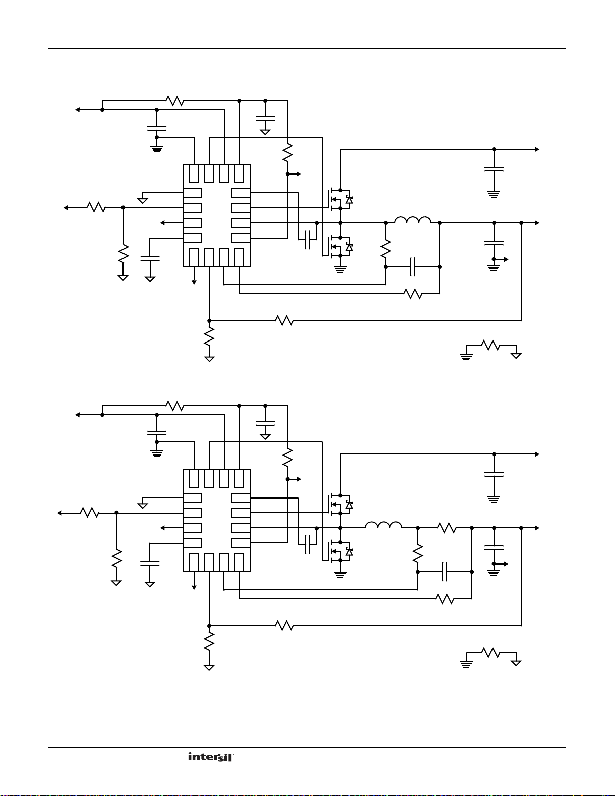
FIGURE 3. ISL95870 APPLICATION SCHEMATIC WITH ONE OUTPUT VOLTAGE SETPOINT AND RESISTOR CURRENT SENSE
3
FN6899.1
December 2, 2013
Page 4
ISL95870, ISL95870A, ISL95870B
VCC
BOOT
UGATE
PHASE
EN
PGOOD
FSEL
VO
PGND
GND
RTN
VID1
VID0
SREF
SET0
SET1
FB
LGATE
PVCC
L
O
C
BOOT
C
SEN
R
OCSET
Q
HS
Q
LS
RTN1
3.3V TO 25V
0.5V TO 5V
R
O
CO
CIN
V
IN
V
OUT
C
SOFT
R
SET1RSET2RSET3
C
VCC
+5V
R
VCC
C
PVCC
GPIO
2
3
4
5
6
7
8
9
19
18
17
16
15
14
13
12
110
11 20
R
PGOOD
OCSET
R
FB
R
OFS
R
OFS1
R
FB1
RTN1
0
VCC
BOOT
UGATE
PHASE
EN
PGOOD
FSEL
VO
PGND
GND
RTN
VID1
VID0
SREF
SET0
SET1
FB
LGATE
PVCC
L
O
C
BOOT
C
SEN
R
OCSET
Q
HS
Q
LS
RTN1
3.3V TO 25V
0.5V TO 5V
R
O
CO
CIN
V
IN
V
OUT
C
SOFT
R
SET1RSET2RSET3
C
VCC
+5V
C
PVCC
GPIO
2
3
4
5
6
7
8
9
19
18
17
16
15
14
13
12
110
11 20
R
PGOOD
OCSET
R
FB
R
OFS
R
SEN
R
OFS1
R
FB1
RTN1
R
VCC
0
Applications Schematics: ISL95870A
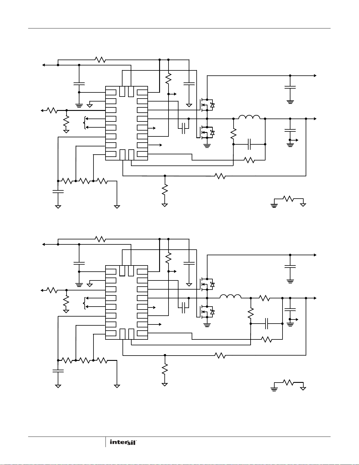
FIGURE 4. ISL95870A APPLICATION SCHEMATIC WITH FOUR OUTPUT VOLTAGE SETPOINTS AND DCR CURRENT SENSE
FIGURE 5. ISL95870A APPLICATION SCHEMATIC WITH FOUR OUTPUT VOLTAGE SETPOINTS AND RESISTOR CURRENT SENSE
4
FN6899.1
December 2, 2013
Page 5
ISL95870, ISL95870A, ISL95870B
VO
BOOT
UGATE
PHASE
EN
PGOOD
FSEL
RTN
VID1
VID0
SREF
SET0
SET1
PVCC
VCC
L
O
C
BOOT
C
SEN
R
OCSET
Q
HS
Q
LS
3.3V TO 25V
0.5V TO 5V
R
O
CO
CIN
V
IN
V
OUT
C
SOFT
C
VCC
+5V
R
VCC
C
PVCC
GPIO
1
2
3
4
5
6
15
14
13
12
11
189
10 17
R
PGOOD
PGND
LGATE
16
7
8
20
19
R
SET1
R
SET2
R
SET3
R
SET4
R
FB
R
OFS
SET2
FB
OCSET
RTN1
R
OFS1
R
FB1
RTN1
GND
0
VO
BOOT
UGATE
PHASE
EN
PGOOD
FSEL
RTN
VID1
VID0
SREF
SET0
SET1
PVCC
VCC
L
O
C
BOOT
C
SEN
R
OCSET
Q
HS
Q
LS
3.3V TO 25V
0.5V TO 5V
R
O
CO
CIN
V
IN
V
OUT
C
SOFT
C
VCC
+5V
R
VCC
C
PVCC
GPIO
1
2
3
4
5
6
15
14
13
12
11
189
10 17
R
PGOOD
PGND
LGATE
16
7
8
20
19
R
SET1
R
SET2
R
SET3
R
SET4
R
FB
R
OFS
SET2
FB
OCSET
R
SEN
RTN1
R
OFS1
R
FB1
RTN1
GND
0
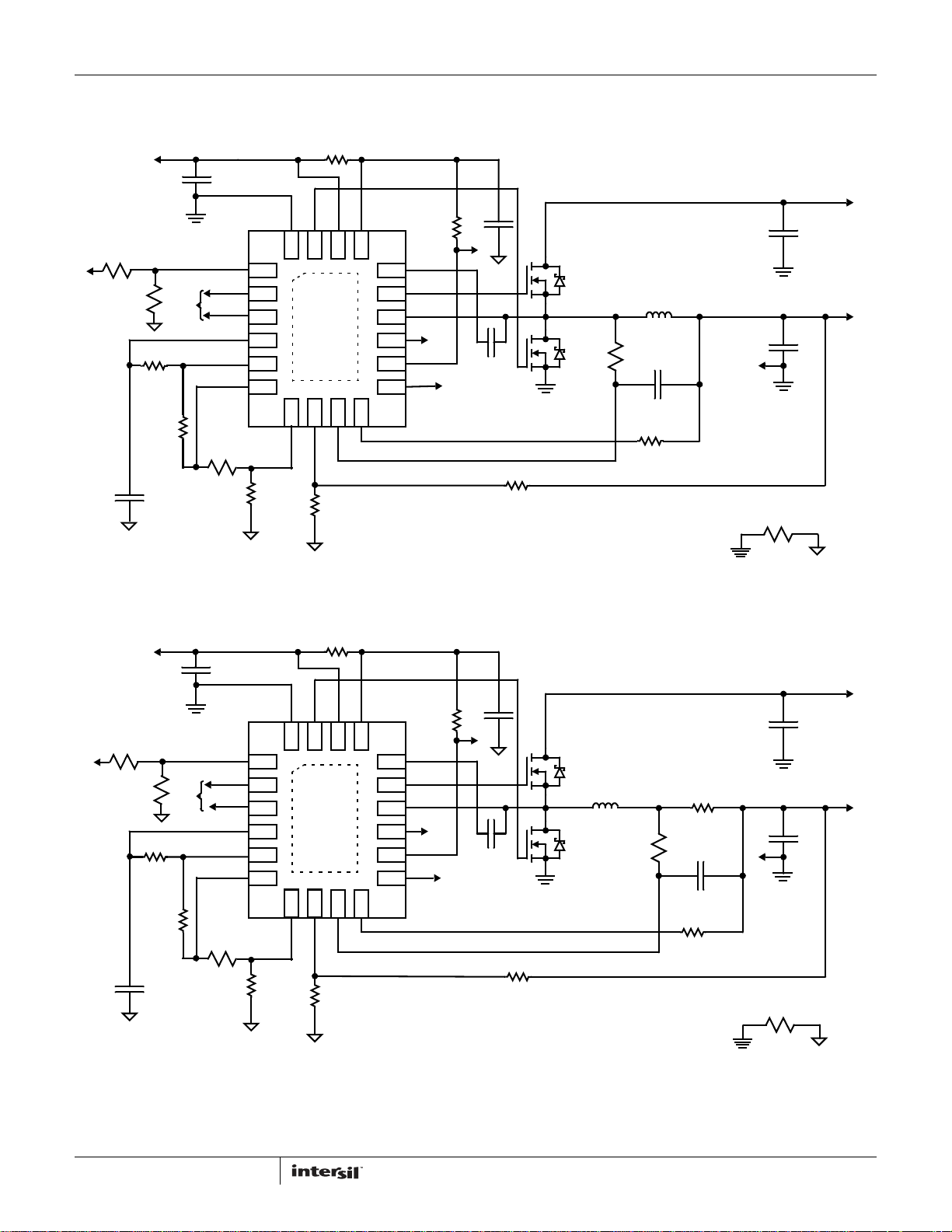
Applications Schematics: ISL95870B
FIGURE 6. ISL95870B APPLICATION SCHEMATIC WITH FOUR OUTPUT VOLTAGE SETPOINTS AND DCR CURRENT SENSE
FIGURE 7. ISL95870B APPLICATION SCHEMATIC WITH FOUR OUTPUT VOLTAGE SETPOINTS AND RESISTOR CURRENT SENSE
5
FN6899.1
December 2, 2013
Page 6
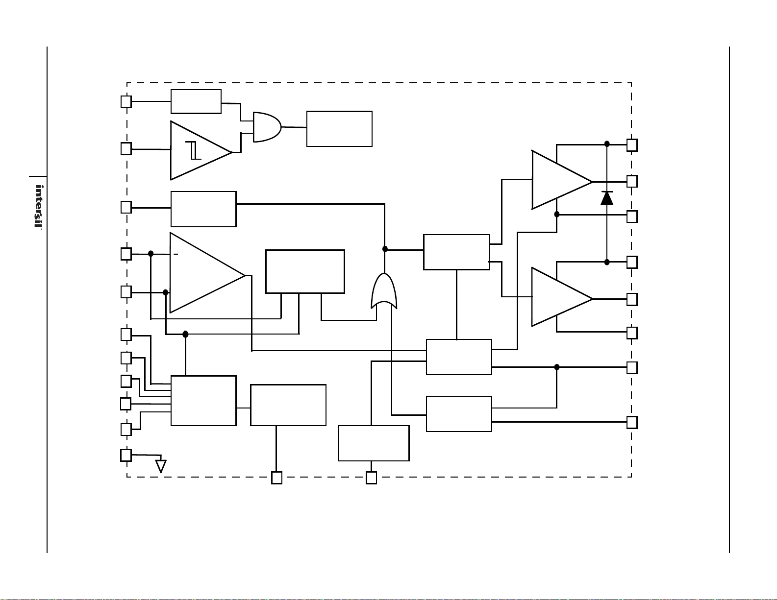
Block Diagram
FIGURE 8. SIMPLIFIED FUNCTIONAL BLOCK DIAGRAM OF ISL95870, ISL95870A, ISL95870B
DRIVER
DRIVER
BOOT
UGATE
PHASE
PVCC
LGATE
PGND
OVERCURRENT
OVERVOLTAGE/
SOFT-START
CIRCUITRY
R
4
MODULATOR
DEAD-TIME
GENERATION
PGOOD
CIRCUITRY
REFERENCE
VOLTAGE
CIRCUITRY
POR
VO
OCSET
*SET 0
*SET 1
**SET2
*VID1
*VID0
FB
PGOOD
SREF
VCC
RTN
EN
INTERNAL
COMPENSATION
AMPLIFIER
+
GND
REMOTE SENSE
CIRCUITRY
FSEL
Fs SELECTION
CIRCUITRY
*ISL95870A, ISL95870B ONLY
**ISL95870B ONLY
UNDERVOLTAGE
6
ISL95870, ISL95870A, ISL95870B
December 2, 2013
FN6899.1
Page 7
Pin Configurations
12
11
10
9
16
15
14
13
5
6
7
8
1
2
3
4
GND
RTN
EN
SREF
BOOT
UGATE
PHASE
PGOOD
PGND
LGATE
PVCC
VCC
FSEL
FB
OCSET
VO
19
18
17
16
15
14
13
1
20
10
11
2
3
4
5
6
7
8
PGND
GND
RTN
VID1
VID0
SREF
SET0
VCC
BOOT
UGATE
PHASE
EN
PGOOD
FSEL
LGATE
PVCC
FB
OCSET
9
SET1
12
VO
10VO
9OCSET
8FB
7SET2
4
SREF
3VID0
1
2
20
PGND
19
LGATE18PVCC
17
VCC
RTN
VID1
5
6
SET0
SET1
16
15
14
13
BOOT
UGATE
PHASE
EN
12
11
PGOOD
FSEL
GND
ISL95870, ISL95870A, ISL95870B
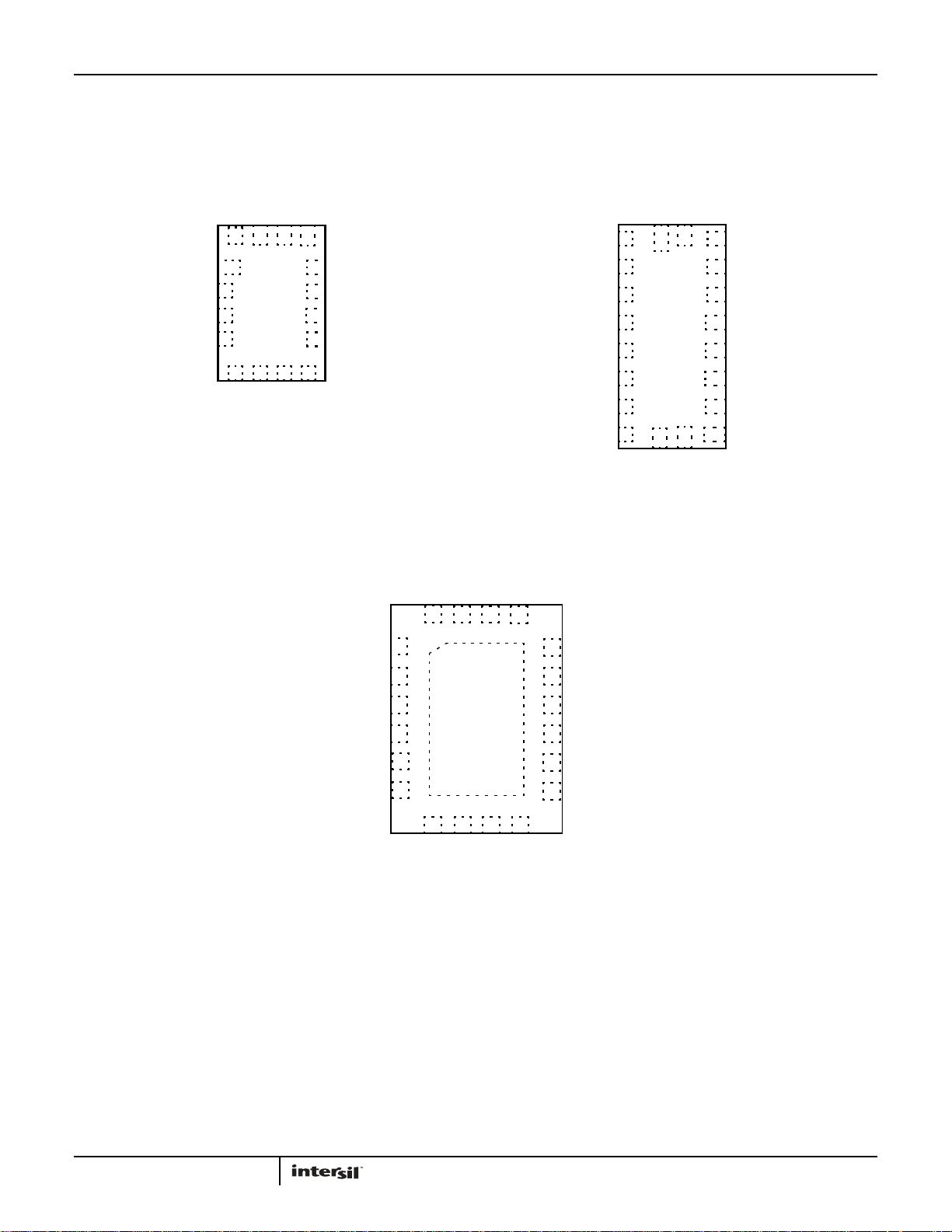
ISL95870
(16 LD 2.6X1.8 µTQFN)
TOP VIEW
ISL95870A
(20 LD 3.2X1.8 µTQFN)
TOP VIEW
ISL95870B
(20 LD 3X4 QFN)
TOP VIEW
7
FN6899.1
December 2, 2013
Page 8

ISL95870, ISL95870A, ISL95870B
ISL95870 Functional Pin Descriptions
PIN NUMBER SYMBOL DESCRIPTION
1 GND IC ground for bias supply and signal reference.
2 RTN Negative remote sense input of V
divider should be used at RTN pin, i.e. keep R
3 EN Enable input for the IC. Pulling EN above the rising threshold voltage initializes the soft-start sequence.
4 SREF Soft-start and voltage slew-rate programming capacitor input. Connects internally to the inverting input of the V
setpoint amplifier.
5 FSEL Input for programming the regulator switching frequency. Pull this pin to VCC for 1MHz switching. Pull this pin to GND
with a 100kΩ resistor for 600kHz switching. Leave this pin floating for 500kHz switching. Pull this pin directly to GND
for 300kHz switching.
6 FB Voltage feedback sense input. Connects internally to the inverting input of the control-loop error amplifier. The converter
is in regulation when the voltage at the FB pin equals the voltage on the SREF pin.
7 OCSET Input for the overcurrent detection circuit. The overcurrent setpoint programming resistor R
pin to the sense node.
8 VO Output voltage sense input for the R
detection circuit.
9 PGOOD Power-good open-drain indicator output. This pin changes to high impedance when the converter is able to supply
regulated voltage.
10 PHASE Return current path for the UGATE high-side MOSFET driver, V
polarity detector input.
11 UGATE High-side MOSFET gate driver output. Connect to the gate terminal of the high-side MOSFET of the converter.
12 BOOT Positive input supply for the UGATE high-side MOSFET gate driver. The BOOT pin is internally connected to the cathode
of the Schottky boot-strap diode. Connect an MLCC between the BOOT pin and the PHASE pin.
13 VCC Input for the IC bias voltage. Connect +5V to the VCC pin and decouple with at least a MLCC to the GND pin.
14 PVCC Input for the LGATE and UGATE MOSFET driver circuits. The PVCC pin is internally connected to the anode of the Schottky
boot-strap diode. Connect +5V to the PVCC pin and decouple with a MLCC to the PGND pin.
15 LGATE Low-side MOSFET gate driver output. Connect to the gate terminal of the low-side MOSFET of the converter.
16 PGND Return current path for the LGATE MOSFET driver. Connect to the source of the low-side MOSFET.
. If resistor divider consisting of RFB and R
OUT
4
modulator. The VO pin also serves as the reference input for the overcurrent
= RFB, and R
FB1
= R
OFS1
IN
OFS
sense input for the R4 modulator, and inductor current
is used at FB pin, the same resistor
OFS
.
connects from this
OCSET
SET
voltage
8
FN6899.1
December 2, 2013
Page 9

ISL95870, ISL95870A, ISL95870B
ISL95870A Functional Pin Descriptions
PIN NUMBER SYMBOL DESCRIPTION
1 LGATE Low-side MOSFET gate driver output. Connect to the gate terminal of the low-side MOSFET of the converter.
2 PGND Return current path for the LGATE MOSFET driver. Connect to the source of the low-side MOSFET.
3 GND IC ground for bias supply and signal reference.
4 RTN Negative remote sense input of V
divider should be used at RTN pin, i.e. keep R
5 VID1 Logic input for setpoint voltage selector. Use in conjunction with the VID0 pin to select among four setpoint reference
voltages.
6 VID0 Logic input for setpoint voltage selector. Use in conjunction with the VID1 pin to select among four setpoint reference
voltages.
7 SREF Soft-start and voltage slew-rate programming capacitor input and setpoint reference voltage programming resistor input.
Connects internally to the inverting input of the V
8 SET0 Voltage set-point programming resistor input.
9 SET1 Voltage set-point programming resistor input.
10 FB Voltage feedback sense input. Connects internally to the inverting input of the control-loop error transconductance
amplifier. The converter is in regulation when the voltage at the FB pin equals the voltage on the SREF pin.
11 OCSET Input for the overcurrent detection circuit. The overcurrent setpoint programming resistor R
pin to the sense node.
12 VO Output voltage sense input for the R
detection circuit.
13 FSEL Input for programming the regulator switching frequency. Pull this pin to VCC for 1MHz switching. Pull this pin to GND
with a 100kΩ resistor for 600kHz switching. Leave this pin floating for 500kHz switching. Pull this pin directly to GND
for 300kHz switching.
14 PGOOD Power-good open-drain indicator output. This pin changes to high impedance when the converter is able to supply
regulated voltage.
15 EN Enable input for the IC. Pulling EN above the rising threshold voltage initializes the soft-start sequence.
16 PHASE Return current path for the UGATE high-side MOSFET driver, V
polarity detector input.
17 UGATE High-side MOSFET gate driver output. Connect to the gate terminal of the high-side MOSFET of the converter.
18 BOOT Positive input supply for the UGATE high-side MOSFET gate driver. The BOOT pin is internally connected to the cathode
of the Schottky boot-strap diode. Connect an MLCC between the BOOT pin and the PHASE pin.
19 VCC Input for the IC bias voltage. Connect +5V to the VCC pin and decouple with at least a MLCC to the GND pin.
20 PVCC Input for the LGATE and UGATE MOSFET driver circuits. The PVCC pin is internally connected to the anode of the Schottky
boot-strap diode. Connect +5V to the PVCC pin and decouple with a MLCC to the PGND pin.
. If resistor divider consisting of RFB and R
OUT
4
modulator. The VO pin also serves as the reference input for the overcurrent
= RFB, and R
FB1
voltage setpoint amplifier.
SET
OFS1
sense input for the R4 modulator, and inductor current
IN
= R
OFS
is used at FB pin, the same resistor
OFS
.
connects from this
OCSET
9
FN6899.1
December 2, 2013
Page 10

ISL95870, ISL95870A, ISL95870B
ISL95870B Functional Pin Descriptions
PIN NUMBER SYMBOL DESCRIPTION
1 RTN Negative remote sense input of V
resistor divider should be used at RTN pin, i.e. keep R
2 VID1 Logic input for setpoint voltage selector. Use in conjunction with the VID0 pin to select among four setpoint reference
voltages.
3 VID0 Logic input for setpoint voltage selector. Use in conjunction with the VID1 pin to select among four setpoint reference
voltages.
4 SREF Soft-start and voltage slew-rate programming capacitor input and setpoint reference voltage programming resistor
input. Connects internally to the inverting input of the V
5 SET0 Voltage set-point programming resistor input.
6 SET1 Voltage set-point programming resistor input.
7 SET2 Voltage set-point programming resistor input.
8 FB Voltage feedback sense input. Connects internally to the inverting input of the control-loop error transconductance
amplifier. The converter is in regulation when the voltage at the FB pin equals the voltage on the SREF pin.
9 OCSET Input for the overcurrent detection circuit. The overcurrent setpoint programming resistor R
pin to the sense node.
10 VO Output voltage sense input for the R
detection circuit.
11 FSEL Input for programming the regulator switching frequency. Pull this pin to VCC for 1MHz switching. Pull this pin to GND
with a 100kΩ resistor for 600kHz switching. Leave this pin floating for 500kHz switching. Pull this pin directly to GND
for 300kHz switching.
12 PGOOD Power-good open-drain indicator output. This pin changes to high impedance when the converter is able to supply
regulated voltage.
13 EN Enable input for the IC. Pulling EN above the rising threshold voltage initializes the soft-start sequence.
14 PHASE Return current path for the UGATE high-side MOSFET driver, V
current polarity detector input.
15 UGATE High-side MOSFET gate driver output. Connect to the gate terminal of the high-side MOSFET of the converter.
16 BOOT Positive input supply for the UGATE high-side MOSFET gate driver. The BOOT pin is internally connected to the
cathode of the Schottky boot-strap diode. Connect an MLCC between the BOOT pin and the PHASE pin.
17 VCC Input for the IC bias voltage. Connect +5V to the VCC pin and decouple with at least a MLCC to the GND pin.
18 PVCC Input for the LGATE and UGATE MOSFET driver circuits. The PVCC pin is internally connected to the anode of the
Schottky boot-strap diode. Connect +5V to the PVCC pin and decouple with a MLCC to the PGND pin.
19 LGATE Low-side MOSFET gate driver output. Connect to the gate terminal of the low-side MOSFET of the converter.
20 PGND Return current path for the LGATE MOSFET driver. Connect to the source of the low-side MOSFET.
Bottom Pad GND IC ground for bias supply and signal reference.
. If resistor divider consisting of RFB and R
OUT
4
modulator. The VO pin also serves as the reference input for the overcurrent
= RFB, and R
FB1
voltage setpoint amplifier.
SET
IN
OFS1
sense input for the R4 modulator, and inductor
is used at FB pin, the same
OFS
= R
.
OFS
OCSET
connects from this
10
FN6899.1
December 2, 2013
Page 11

ISL95870, ISL95870A, ISL95870B
Ordering Information
PART NUMBER
(Note 2)
ISL95870HRUZ-T (Notes 1, 4) GAV -10 to +100 16 Ld 2.6x1.8 µTQFN L16.2.6x1.8A
ISL95870AHRUZ-T (Notes 1, 4) GAW -10 to +100 20 Ld 3.2x1.8 µTQFN L20.3.2x1.8
ISL95870BHRZ (Note 3) 870B -10 to +100 20 Ld 3x4 QFN L20.3x4
ISL95870BHRZ-T (Notes 1, 3) 870B -10 to +100 20 Ld 3x4 QFN L20.3x4
ISL95870IRUZ-T (Notes 1, 4) GAZ -40 to +100 16 Ld 2.6x1.8 µTQFN L16.2.6x1.8A
ISL95870AIRUZ-T (Notes 1, 4) GAX -40 to +100 20 Ld 3.2x1.8 µTQFN L20.3.2x1.8
ISL95870BIRZ (Note 3) 870I -40 to +100 20 Ld 3x4 QFN L20.3x4
ISL95870BIRZ-T (Notes 1, 3) 870I -40 to +100 20 Ld 3x4 QFN L20.3x4
NOTES:
1. Please refer to TB347
2. For Moisture Sensitivity Level (MSL), please see device information page for ISL95870
see techbrief TB363
3. These Intersil Pb-free plastic packaged products employ special Pb-free material sets, molding compounds/die attach materials, and 100% matte
tin plate plus anneal (e3 termination finish, which is RoHS compliant and compatible with both SnPb and Pb-free soldering operations). Intersil
Pb-free products are MSL classified at Pb-free peak reflow temperatures that meet or exceed the Pb-free requirements of IPC/JEDEC J STD-020.
4. These Intersil Pb-free plastic packaged products employ special Pb-free material sets; molding compounds/die attach materials and NiPdAu plate
- e4 termination finish, which is RoHS compliant and compatible with both SnPb and Pb-free soldering operations. Intersil Pb-free products are MSL
classified at Pb-free peak reflow temperatures that meet or exceed the Pb-free requirements of IPC/JEDEC J STD-020.
for details on reel specifications.
.
PART
MARKING
TEMP RANGE
(°C)
PACKAGE
(Pb-Free)
, ISL95870A,ISL95870B. For more information on MSL please
PKG.
DWG. #
11
FN6899.1
December 2, 2013
Page 12

ISL95870, ISL95870A, ISL95870B
Absolute Maximum Ratings Thermal Information
VCC, PVCC, PGOOD, FSEL to GND. . . . . . . . . . . . . . . . . . . . . . -0.3V to +7.0V
VCC, PVCC to PGND . . . . . . . . . . . . . . . . . . . . . . . . . . . . . . . . . -0.3V to +7.0V
GND to PGND . . . . . . . . . . . . . . . . . . . . . . . . . . . . . . . . . . . . . . -0.3V to +0.3V
EN, SET0, SET1, SET2, VO,
VID0, VID1, FB, RTN, OCSET, SREF . . . . . . . . . . . . -0.3V to GND, VCC + 0.3V
BOOT Voltage (V
BOOT To PHASE Voltage (V
BOOT-GND
) . . . . . . . . . . . . . . . . . . . . . . . . . . . . . -0.3V to 33V
BOOT-PHASE
). . . . . . . . . . . . . . . . -0.3V to 7V (DC)
-0.3V to 9V (<10ns)
PHASE Voltage . . . . . . . . . . . . . . . . . . . . . . . . . . . . . . . . . . GND - 0.3V to 28V
GND -8V (<20ns Pulse Width, 10µJ)
UGATE Voltage. . . . . . . . . . . . . . . . . . . . . . . . . . V
V
- 5V (<20ns Pulse Width, 10µJ) to V
LGATE Voltage . . . . . . . . . . . . . . . . . . . . . . . . . GND - 0.3V (DC) to VCC + 0.3V
PHASE
- 0.3V (DC) to V
PHASE
BOOT
BOOT
. . . . . . . . . . . . . . . . . . GND - 2.5V (<20ns Pulse Width, 5µJ) to VCC + 0.3V
ESD Rating
Human Body Model . . . . . . . . . . . . . . . . . . . . . . . . . . . . . . . . . . . . . . . . 2kV
Machine Model . . . . . . . . . . . . . . . . . . . . . . . . . . . . . . . . . . . . . . . . . . . 200V
Charged Device Model . . . . . . . . . . . . . . . . . . . . . . . . . . . . . . . . . . . . . . 1kV
Latch Up. . . . . . . . . . . . . . . . . . . . . . . . . . . JEDEC Class II Level A at +125°C
CAUTION: Do not operate at or near the maximum ratings listed for extended periods of time. Exposure to such conditions may adversely impact product
reliability and result in failures not covered by warranty.
ΝΟΤΕΣ:
5. θ
is measured with the component mounted on a high effective thermal conductivity test board in free air. See Tech Brief TB379 for details.
JA
is measured in free air with the component mounted on a high effective thermal conductivity test board with “direct attach” features. See Tech
6. θ
JA
Brief TB379
7. F or θ
.
, the “case temp” location is the center of the exposed metal pad on the package underside.
JC
Thermal Resistance (Typical) θ
(°C/W) θJC (°C/W)
JA
16 Ld UTQFN (Note 5) . . . . . . . . . . . . . . . . . 90 N/A
20 Ld UTQFN (Note 5) . . . . . . . . . . . . . . . . . 88 N/A
20 Ld QFN (Notes 6, 7) . . . . . . . . . . . . . . . . 44 5
Junction Temperature Range . . . . . . . . . . . . . . . . . . . . . . . -55°C to +150°C
Operating Temperature Range:
For “H” Version Parts . . . . . . . . . . . . . . . . . . . . . . . . . . . . . . -10°C to +100°C
For “I” Version Parts . . . . . . . . . . . . . . . . . . . . . . . . . . . . . . .-40°C to +100°C
Storage Temperature. . . . . . . . . . . . . . . . . . . . . . . . . . . . . .-65°C to +150°C
Pb-Free Reflow Profile . . . . . . . . . . . . . . . . . . . . . . . . . . . . . . . see link below
http://www.intersil.com/pbfree/Pb-FreeReflow.asp
Recommended Operating Conditions
Ambient Temperature Range:
For “H” Version Parts . . . . . . . . . . . . . . . . . . . . . . . . . . . . . . -10°C to +100°C
For “I” Version Parts . . . . . . . . . . . . . . . . . . . . . . . . . . . . . . .-40°C to +100°C
Converter Input Voltage to GND . . . . . . . . . . . . . . . . . . . . . . . . . 3.3V to 25V
VCC, PVCC to GND. . . . . . . . . . . . . . . . . . . . . . . . . . . . . . . . . . . . . . . . . 5V ±5%
Electrical Specifications All typical specifications T
-40°C to +100°C, unless otherwise stated.
PARAMETER SYMBOL TEST CONDITIONS
VCC and PVCC
VCC Input Bias Current I
VCC Shutdown Current I
PVCC Shutdown Current I
PVCCoff
VCC POR THRESHOLD
Rising VCC POR Threshold Voltage V
Falling VCC POR Threshold Voltage
VCC_THR
V
VCC_THF
REGULATION
System Accuracy
PWM
Switching Frequency Accuracy F
VO
VO Input Impedance R
VO Reference Offset Current I
VO Input Leakage Current I
VCCoff
VOSSVENTHR
VOoff
EN = 5V, VCC = 5V, FB = 0.55V, SREF < FB - 1.2 1.9 mA
VCC
EN = GND, VCC = 5V - 0 1.0 µA
EN = GND, PVCC = 5V - 0 1.0 µA
VID0 = VID1 = VCC, PWM Mode = CCM
(For “H” Version Parts, T
VID0 = VID1 = VCC, PWM Mode = CCM -0.75 +0.5 %
PWM Mode = CCM
(For “H” Version Parts, T
SW
PWM Mode = CCM -22 - +15 %
EN = 5V - 600 - kΩ
VO
EN = GND, VO = 3.6V - 0 - µA
= +25°C, VCC = 5V. Boldface limits apply over the operating temperature range,
A
MIN
(Note 11) TYP
MAX
(Note 11) UNIT
4.40 4.52 4.60 V
4.10 4.22 4.35 V
-0.5 - +0.5 %
= -10°C to +100°C)
A
-15 - +15 %
= -10°C to +100°C)
A
< EN, SREF = Soft-Start Mode - 8.5 - µA
12
FN6899.1
December 2, 2013
Page 13

ISL95870, ISL95870A, ISL95870B
Electrical Specifications All typical specifications T
-40°C to +100°C, unless otherwise stated. (Continued)
PARAMETER SYMBOL TEST CONDITIONS
ERROR AMPLIFIER
FB Input Bias Current I
SREF (Note 8)
Soft-Start Current I
Voltage Step Current I
POWER GOOD
PGOOD Pull-down Impedance R
PGOOD Leakage Current I
GATE DRIVER
UGATE Pull-Up Resistance (Note 9) R
UGATE Source Current (Note 9) I
UGSRC
UGATE Sink Resistance (Note 9) R
UGATE Sink Current (Note 9) I
UGSNK
LGATE Pull-Up Resistance (Note 9) R
LGATE Source Current (Note 9) I
LGSRC
LGATE Sink Resistance (Note 9) R
LGATE Sink Current (Note 9) I
UG ATE to LGAT E De adtim e t
LGATE to UGAT E De adtim e t
LGSNK
UGFLGR
LGFUGR
PHASE
PHASE Input Impedance R
PHASE
BOOTSTRAP DIODE
Forward Voltage V
Reverse Leakage I
CONTROL INPUTS
EN High Threshold Voltage V
EN Low Threshold Voltage V
ENTHR
ENTHF
EN Input Bias Current I
EN Leakage Current I
VID<0,1> High Threshold Voltage (Note 10) V
VID<0,1> Low Threshold Voltage
(Note 10)
ENoff
VIDTHR
V
VIDTHF
VID<0,1> Input Bias Current (Note 10) I
VID<0,1> Leakage Current (Note 10) I
VIDoff
PROTECTION
OCP Threshold Voltage V
OCPTHVOCSET
UGPU
UGPD
LGPU
LGPD
EN = 5V, FB = 0.50V -20 - +50 nA
FB
SREF = Soft-Start Mode 8.5 17 25.5 µA
SS
SREF = Setpoint-Stepping Mode
(For “H” Version Parts, T
VS
SREF = Setpoint-Stepping Mode ±46 ±85 ±127 µA
PGOOD = 5mA Sink - 50 150 Ω
PG
PGOOD = 5V - 0.1 1.0 µA
PG
200mA Source Current - 1.1 1.7 Ω
UGATE - PHASE = 2.5V - 1.8 - A
250mA Sink Current - 1.1 1.7 Ω
UGATE - PHASE = 2.5V - 1.8 - A
250mA Source Current - 1.1 1.7 Ω
LGATE - GND = 2.5V - 1.8 - A
250mA Sink Current - 0.55 1.0 Ω
LGATE - PGND = 2.5V - 3.6 - A
UGATE falling to LGATE rising, no load - 21 - ns
LGATE falling to UGATE rising, no load - 21 - ns
PVCC = 5V, IF = 2mA - 0.58 - V
F
VR = 25V - 0 - µA
R
EN = 5V 0.85 1.7 2.55 µA
EN
EN = GND - 0 1.0 µA
EN = 5V - 0.5 - µA
VID
EN=0V - 0 - µA
= +25°C, VCC = 5V. Boldface limits apply over the operating temperature range,
A
MIN
(Note 11) TYP
MAX
(Note 11) UNIT
±51 85 ±119 µA
= -10°C to +100°C)
A
- 33 - kΩ
2.0 - - V
- - 1.0 V
0.65 - - V
- - 0.5 V
- V
O
-1.75 - 1.75 mV
13
FN6899.1
December 2, 2013
Page 14

ISL95870, ISL95870A, ISL95870B
Electrical Specifications All typical specifications T
-40°C to +100°C, unless otherwise stated. (Continued)
PARAMETER SYMBOL TEST CONDITIONS
EN = 5.0V
OCP Reference Current I
OCSET Input Resistance R
OCSET Leakage Current I
UVP Threshold Voltage V
OVP Rising Threshold Voltage V
OVP Falling Threshold Voltage V
OTP Rising Threshold Temperature
(Note 9)
OTP Hysteresis (Note 9) T
NOTES:
8. For ISL95870,there is one internal reference 0.5V. For ISL95870A, ISL95870B, there are four resistor-programmed reference voltages.
9. Limits established by characterization and are not production tested.
10. VID function is only for ISL95870A, ISL95870B.
11. Parameters with MIN and/or MAX limits are 100% tested at +25°C, unless otherwise specified. Temperature limits established by characterization
and are not production tested.
OCSET
OCSET
UVTHVFB
OVRTH
OVFTHVFB
T
OTRTH
OTHYS
(For “H” Version Parts, T
OCP
EN = 5.0V 7. 05 8.5 9.35 µA
EN = 5.0V - 600 - kΩ
EN = GND - 0 - µA
VFB = %V
(For “H” Version Parts, TA = -10°C to +100°C)
VFB = %V
= +25°C, VCC = 5V. Boldface limits apply over the operating temperature range,
A
MIN
= %V
= %V
SREF
SREF
SREF
SREF
= -10°C to +100°C)
A
(Note 11) TYP
7. 65 8.5 9.35 µA
81 84 87 %
113 116 120 %
112.5 116 120 %
98 102 106 %
- 150 - °C
- 25 - °C
(Note 11) UNIT
MAX
14
FN6899.1
December 2, 2013
Page 15

ISL95870, ISL95870A, ISL95870B
t
SS
V
SREFCSOFT
⋅
I
SS
-------------------------------------------
=
(EQ. 1)
C
SOFT
tSSISS⋅
V
SREF
---------------------- -
=
(EQ. 2)
RTR
SET1RSET2
…R
SET n()
++=
(EQ. 3)
t
SS
RTC
SOFT
⋅()– LN 1
V
START-UP
ISSRT⋅
------------------------------
–()⋅=
(EQ. 4)
t
VS
RTC
SOFT
⋅()– LN 1
V
NEWVOLD
–()
I
VSRT
⋅
-------------------------------------------
–()⋅=
(EQ. 5)
Theory of Operation
The following sections will provide a detailed description of the
inner workings of the ISL95870, ISL95870A, ISL95870B.
Power-On Reset
The IC is disabled until the voltage at the VCC pin has increased
above the rising power-on reset (POR) threshold voltage
V
VCC_THR
at the VCC pin decreases below the falling POR threshold voltage
V
VCC_THF
1µs.
Start-Up Timing
Once VCC has ramped above V
enabled by pulling the EN pin voltage above the input-high
threshold V
SREF pin begins slewing to the designated VID set-point. The
converter output voltage at the FB feedback pin follows the
voltage at the SREF pin. During soft-start, The regulator always
operates in CCM until the soft-start sequence is complete.
Start-Up and Voltage-Step Operation for
ISL95870
When the voltage on the VCC pin has ramped above the rising
power-on reset voltage V
has increased above the rising enable threshold voltage
the SREF pin releases its discharge clamp, and enables the
reference amplifier V
17µA and is sourced out of the SREF pin and charges capacitor
C
SOFT
such that the voltage on the FB pin tracks the rising voltage on
the SREF pin. The elapsed time from when the EN pin is asserted
to when V
delay tSS which is given by Equation 1:
. The controller will become disabled when the voltage
. The POR detector has a noise filter of approximately
, the controller can be
, and the voltage on the EN pin
to V
is called the soft-start
REF
until V
SREF
VCC_THR
. Approximately 20µs later, the voltage at the
ENTHR
VCC_THR
. The soft-start current ISS is limited to
SET
equals V
SREF
has charged C
. The regulator controls the PWM
REF
SOFT
V
ENTHR
,
Start-Up and Voltage-Step Operation for
ISL95870A, ISL95870B
When the voltage on the VCC pin has ramped above the rising
power-on reset voltage V
VCC_THR
has increased above the rising enable threshold voltage V
the SREF pin releases its discharge clamp and enables the
reference amplifier V
. The soft-start current ISS is limited to
SET
17µA and is sourced out of the SREF pin into the parallel RC
network of capacitor C
SOFT
is the sum of all the series connected R
resistors and is written as Equation 3:
The voltage on the SREF pin rises as I
voltage reference setpoint selected by the state of the VID inputs at
the time the EN pin is asserted. The regulator controls the PWM
such that the voltage on the FB pin tracks the rising voltage on the
SREF pin. Once C
charges to the selected setpoint voltage, the
SOFT
ISS current source comes out of the 17µA current limit and decays
to the static value set by V
SREF/RT
EN pin is asserted to when V
setpoint is the soft-start delay tSS which is given by Equation 4:
Where:
is the soft-start current source at the 17µA limit
- I
SS
-V
START-UP
is the setpoint reference voltage selected by the
state of the VID inputs at the time EN is asserted
is the sum of the R
-R
T
The end of soft-start is detected by I
capacitor C
charges to the designated V
SOFT
reference setpoint. The SSOK flag is set, and the PGOOD pin goes
high.
, and the voltage on the EN pin
ENTHR
and resistance RT. The resistance RT
programming
SET
charges C
SS
SOFT
to the
. The elapsed time from when the
has reached the voltage reference
SREF
programming resistors
SET
tapering off when
SS
SET
voltage
,
Where:
-I
is the soft-start current source at the 17µA limit
SS
-V
The end of soft-start is detected by I
capacitor C
is the buffered V
SREF
charges to V
SOFT
reference voltage
REF
tapering off when
SS
. The internal SSOK flag is set,
REF
the PGOOD pin goes high, and diode emulation mode (DEM) is
enabled.
Choosing the C
particular soft-start delay t
capacitor to meet the requirements of a
SOFT
is calculated using Equation 2,
SS
which is written as follows:
Where:
-tSS is the soft-start delay
is the soft-start current source at the 17µA limit
-I
SS
-V
Choosing the C
particular soft-start delay t
is the buffered V
SREF
SOFT
reference voltage
REF
capacitor to meet the requirements of a
is calculated with Equation 6,
SS
15
The ISS current source changes over to the voltage-step current
source IVS which has a current limit of ±85µA. Whenever the VID
inputs or the external setpoint reference programs a different
setpoint reference voltage, the I
discharges capacitor C
charges to the selected setpoint voltage, the IVS current
C
SOFT
SOFT
current source charges or
VS
to that new level at ±85µA. Once
source comes out of the 85µA current limit and decays to the
static value set by V
SREF/RT
to the new voltage is called the voltage-step delay t
. The elapsed time to charge C
and is
VS
SOFT
given by Equation 5:
Where:
is the ±85µA setpoint voltage-step current; positive
- I
VS
when V
-V
NEW
-V
OLD
is the sum of the R
-R
T
> V
NEW
, negative when V
OLD
NEW
< V
OLD
is the new setpoint voltage selected by the VID inputs
is the setpoint voltage that V
programming resistors
SET
is changing from
NEW
FN6899.1
December 2, 2013
Page 16

ISL95870, ISL95870A, ISL95870B
C
SOFT
tSS–
R
T
LN 1
V
START-UP
ISSRT⋅
------------------------------
–()⋅
⎝⎠
⎜⎟
⎛⎞
---------------------------------------------------------------------
=
(EQ. 6)
C
SOFT
tVS–
R
T
LN 1
V
NEWVOLD
–
I
VSRT
⋅
-------------------------------------- -
–()⋅
⎝⎠
⎜⎟
⎛⎞
------------------------------------------------------------------------------
=
(EQ. 7)
V
OUTVSREF
RFBR
OFS
+
R
OFS
----------------------------------
⋅=
(EQ. 8)
FIGURE 9. ISL95870 VOLTAGE PROGRAMMING CIRCUIT
SREF
V
SET
+
-
V
REF
C
SOFT
EA
+
-
FB
R
OFS
R
FB
V
OUT
V
COMP
V
SETXVREF
1
R
F
R
IN
--------- -
+
⎝⎠
⎜⎟
⎛⎞
⋅=
(EQ. 9)
V
SET1VREF
=
(EQ. 10)
V
SET2VREF
1
R
SET1
R
SET2RSET3
+
--------------------------------------------
+
⎝⎠
⎜⎟
⎛⎞
⋅=
(EQ. 11)
V
SET3VREF
1
R
SET1RSET2
+
R
SET3
--------------------------------------------
+
⎝⎠
⎜⎟
⎛⎞
⋅=
(EQ. 12)
V
SET4VREF
1
R
SET1
R
SET2
------------------
+
⎝⎠
⎜⎟
⎛⎞
⋅=
(EQ. 13)
which is written as:
Where:
is the soft-start delay
-t
SS
is the soft-start current source at the 17µA limit
-I
SS
-V
START-UP
is the setpoint reference voltage selected by the
state of the VID inputs at the time EN is asserted
is the sum of the R
-R
T
Choosing the C
capacitor to meet the requirements of a
SOFT
programming resistors
SET
particular voltage-step delay tVS is calculated with Equation 7,
which is written as:
Where:
is the voltage-step delay
- t
VS
-V
-V
- I
-RT is the sum of the R
is the new setpoint voltage
NEW
is the setpoint voltage that V
OLD
is the ±85µA setpoint voltage-step current; positive
VS
when V
NEW
> V
, negative when V
OLD
programming resistors
SET
is changing from
NEW
< V
NEW
OLD
Output Voltage Programming for ISL95870
The ISL95870 has a fixed 0.5V reference voltage (V
shown in Figure 9, the output voltage is the reference voltage if
is shorted and R
R
FB
R
and RFB allows the user to scale the output voltage
OFS
is open. A resistor divider consisting of
OFS
between 0.5V and 5V. The relation between the output voltage
and the reference voltage is given in Equation 8:
SREF
). As
Output Voltage Programming for ISL95870A
The ISL95870A allows the user to select four different reference
voltages, thus four different output voltages, by voltage
identification pins VID1 and VID0. The maximum reference voltage
cannot be designed high er than 1.5V. The implementation scheme
is shown in Figure 10. The setpoint reference voltages are
programmed with resistors that use the naming convention
where (x) is the first, second, or third programming resistor
R
SET(x)
connected in series starting at the SREF pin and ending at the GND
pin. As shown in Table 1, different combinations of VID1 and VID0
closes different switches and leaves other switches open. For
example, for the case of VID1 = 1 and VID0 = 0, switch SW1 closes
and all the other three switches SW0, SW2 and SW3 are open. For
one combination of VID1 and VID0, the internal switch connects
the inverting input of the V
the string of R
programming resistors. All the resistors between
SET
that node and the SREF pin serve as the feedback impedance RF
of the V
amplifier. Likewise, all the resistors between that node
SET
and the GND pin serve as the input impedance RIN of the V
amplifier. Equation 9 gives the general form of the gain equation
for the V
amplifier:
SET
Where:
-V
is the 0.5V internal reference of the IC
REF
is the resulting setpoint reference voltage that
-V
SETx
appears at the SREF pin
TABLE 1. ISL95870A VID TRUTH TABLE
VID STATE RESULT
VID1 VID0 CLOSE V
11SW0V
10SW1V
01SW2V
00SW1, SW3V
amplifier to a specific node among
SET
SREF
SET1
SET2
SET3
SET4
V
V
V
V
SET
V
OUT
OUT1
OUT2
OUT3
OUT4
16
Equations 10, 11, 12 and 13 give the specific V
equations for
SET
the ISL95870A setpoint reference voltages.
The ISL95870A V
The ISL95870A V
The ISL95870A V
The ISL95870A V
The V
is fixed at 0.5V because it corresponds to the closure
SET1
of internal switch SW0 that configures the V
setpoint is written as Equation 10:
SET1
setpoint is written as Equation 11:
SET2
setpoint is written as Equation 12:
SET3
setpoint is written as Equation 13:
SET4
SET
amplifier as a
FN6899.1
December 2, 2013
Page 17

ISL95870, ISL95870A, ISL95870B
V
SET1VSET2
⋅ V+
SET3
V
SET4
⋅ V–
SET2VSET3
⋅ V–
SET2VSET4
⋅ 0=
(EQ. 14)
R
SET1
R
SET3VSET4VREF
–()V
SET2VREF
–()⋅⋅
V
REFVSET4VSET2
–()⋅
---------------------------------------------------------------------------------------------------------------------
=
(EQ. 15)
R
SET2
R
SET3VSET2VREF
–()⋅
V
SET4VSET2
–
------------------------------------------------------------------- -
=
(EQ. 16)
R
SET1RSET2RSET3
++ 300kΩ≅
(EQ. 17)
FIGURE 10. ISL95870A VOLTAGE PROGRAMMING CIRCUIT
SET0
SREF
V
SET
+
-
SW0
VREF
SET1
SW1
SW2
SW3
CSOFT
RSET1RSET2RSET3
EA
+
-
FB
ROFS
RFBVOUT
VCOMP
0.5V
V
OUTVSREF
RFBR
OFS
+
R
OFS
----------------------------------
⋅ V
SREF
k⋅==
(EQ. 18)
V
OUTxVSETx
k⋅=
(EQ. 19)
V
SETXVREF
1
R
F
R
IN
--------- -
+
⎝⎠
⎜⎟
⎛⎞
⋅=
(EQ. 20)
V
SET1VREF
=
(EQ. 21)
V
SET2VREF
1
R
SET1
R
SET2RSET3RSET4
++
---------------------------------------------------------------------
+
⎝⎠
⎜⎟
⎛⎞
⋅=
(EQ. 22)
unity-gain voltage follower for the 0.5V voltage reference V
Theoretically, V
depending on the selection of R
can be higher or lower or equal to V
SET3
SET1
, R
SET2
and R
SET3
.
REF
SET4
. However,
it is recommended to design the four reference voltages in the
following order:
SET1
OUT1
< V
< V
-V
-V
For given four user selected reference voltages V
SET2
OUT2
< V
< V
SET3
OUT3
< V
< V
SET4
OUT4
Thus,
SETx
, the
following equation needs to be satisfied in order to have non-zero
solution for R
The programmed resistors R
in the following way. First, assign an initial value to R
approximately 100kΩ then calculate R
SETx
.
, R
SET1
SET2
and R
SET1
SET3
and R
are designed
of
SET3
using
SET2
Equations 15 and 16 respectively.
The sum of all the programming resistors should be
approximately 300kΩ, as shown in Equation 17, otherwise adjust
the value of R
and repeat the calculations.
SET3
R
allows the user to program the output voltage in the range
OFS
of 1.5V to 5V. The relation between the output voltage and the
reference voltage is given in Equation 18:
In this case, the four output voltages are equal to each of the
corresponding reference voltages multiplying the factor k.
Output Voltage Programming for ISL95870B
The ISL95870B allows the user to select four different reference
voltages, thus four different output voltages, by voltage
identification pins VID1 and VID0. The maximum reference
voltage cannot be designed higher than 1.5V. The
implementation scheme is shown in Figure 11. The setpoint
reference voltages are programmed with resistors that use the
naming convention R
fourth programming resistor connected in series starting at the
SREF pin and ending at the GND pin. As shown in Table 2,
different combinations of VID1 and VID0 close different switches
and leave other switches open. For example, for the case of
VID1 = 1 and VID0 = 0, switch SW1 closes and all the other three
switches SW0, SW2 and SW3 are open. For one combination of
VID1 and VID0, the internal switch connects the inverting input of
the V
amplifier to a specific node among the string of R
SET
programming resistors. All the resistors between that node and
the SREF pin serve as the feedback impedance R
amplifier. Likewise, all the resistors between that node and the
GND pin serve as the input impedance R
Equation 20 gives the general form of the gain equation for the
V
amplifier:
SET
where (x) is the first, second, third, or
SET(x)
of the V
F
of the V
IN
SET
SET
SET
amplifier.
If the output voltage is in the range of 0.5V to 1.5V, the external
resistor-divider is not necessary. The output voltage is equal to
one of the reference voltages depending on the status of VID1
and VID0. The external resistor divider consisting of R
FB
and
Where:
-V
is the 0.5V internal reference of the IC
REF
-V
is the resulting setpoint reference voltage that
SETx
appears at the SREF pin
TABLE 2. ISL95870B VID TRUTH TABLE
VID STATE RESULT
VID1 VID0 CLOSE V
11SW0V
10SW1V
01SW2V
00SW3V
SREF
SET1
SET2
SET3
SET4
Equations 21, 22, 23 and 24 give the specific V
the ISL95870B setpoint reference voltages.
The ISL95870B V
The ISL95870B V
setpoint is written as Equation 21:
SET1
setpoint is written as Equation 22:
SET2
V
V
V
V
equations for
SET
V
OUT
OUT1
OUT2
OUT3
OUT4
17
FN6899.1
December 2, 2013
Page 18

ISL95870, ISL95870A, ISL95870B
V
SET3VREF
1
R
SET1RSET2
+
R
SET3RSET4
+
--------------------------------------------
+
⎝⎠
⎜⎟
⎛⎞
⋅=
(EQ. 23)
V
SET4VREF
1
R
SET1RSET2
R+
SET3
+
R
SET4
---------------------------------------------------------------------
+
⎝⎠
⎜⎟
⎛⎞
⋅=
(EQ. 24)
R
SET1
R
SET4VSET4VSET2VREF
–()⋅⋅
V
REFVSET2
⋅
-------------------------------------------------------------------------------------------
=
(EQ. 25)
R
SET2
R
SET4VSET4VSET3VSET2
–()⋅⋅
V
SET2VSET3
⋅
----------------------------------------------------------------------------------------------
=
(EQ. 26)
R
SET3
R
SET4VSET4VSET3
–()⋅
V
SET3
---------------------------------------------------------------------- -
=
(EQ. 27)
R
SET1RSET2RSET3RSET4
+++ 300kΩ≅
(EQ. 28)
V
OUTVSREF
RFBR
OFS
+
R
OFS
----------------------------------
⋅ V
SREF
k⋅==
(EQ. 29)
V
OUTxVSETx
k⋅=
(EQ. 30)
FIGURE 11. ISL95870B VOLTAGE PROGRAMMING CIRCUIT
SET2
SET0
SREF
V
SET
+
-
SW0
VREF
SET1
SW1
SW2
SW3
CSOFT
RSET1RSET2RSET3RSET4
EA
+
-
FB
ROFS
RFBVOUT
VCOMP
0.5V
The ISL95870B V
The ISL95870B V
The V
is fixed at 0.5V because it corresponds to the closure
SET1
of internal switch SW0 that configures the V
setpoint is written as Equation 23:
SET3
setpoint is written as Equation 24:
SET4
SET
amplifier as a
unity-gain voltage follower for the 0.5V voltage reference V
The setpoint reference voltages use the naming convention
V
where (x) is the first, second, third, or fourth setpoint
SET(x)
reference voltage where:
SET1
OUT1
< V
< V
-V
-V
For given four user selected reference voltages V
programmed resistors R
SET2
OUT2
< V
< V
SET3
OUT3
SET1
< V
< V
, R
SET4
OUT4
SET2
, R
thus,
SET3
and R
SETx
SET4
, the
are
designed in the following way. First, assign an initial value to R
of approximately 100kΩ then calculate R
SET1, RSET2
and R
using Equations 25, 26, and 27 respectively.
REF
SET4
SET3
.
The sum of all the programming resistors should be
approximately 300kΩ, as shown in Equation 28, otherwise
adjust the value of R
and repeat the calculations.
SET4
If the output voltage is in the range of 0.5V to 1.5V, the external
resistor-divider is not necessary. The output voltage is equal to
one of the reference voltages depending on the status of VID1
and VID0. The external resistor divider consisting of R
allows the user to program the output voltage in the range
R
OFS
of 1.5V to 5V. The relation between the output voltage and the
reference is given in Equation 29:
In this case, the four output voltages are equal to each of the
corresponding reference voltages multiplying the factor k.
FB
and
High Output Voltage Programming
The ISL95870 has a fixed 0.5V reference voltage (V
high output voltage application, the resistor divider consisting of
R
FB
and R
requires large ratio (RFB :R
OFS
= 9:1 for 5V
OFS
output). The FB pin with large ratio resistor divider is noise
sensitive and the PCB layout should be carefully routed. It is
recommended to use small value resistor divider such as
=1kΩ.
R
FB
In general the ISL95870A and ISL95870B have much better
jitter performance than the ISL95870 when the output voltage is
in the range of 3.3V to 5V, particularly in DCM. This is because
V
voltage can be set to 1.5V and a smaller ratio resistor
SREF
divider can be used. This makes the singal to noise ratio at FB pin
much better. So for 3.3V to 5V output, the ISL95870A and
ISL95870B are recommended with V
set to 1.5V.
SREF
SREF
). For
R4 Modulator
The R4 modulator is an evolutionary step in R3 technology. Like
3
R
, the R4 modulator allows variable frequency in response to
load transients and maintains the benefits of current-mode
hysteretic controllers. However, in addition, the R
reduces regulator output impedance and uses accurate
referencing to eliminate the need for a high-gain voltage
amplifier in the compensation loop. The result is a topology that
can be tuned to voltage-mode hysteretic transient speed while
maintaining a linear control model and removes the need for any
compensation. This greatly simplifies the regulator design for
customers and reduces external component cost.
4
modulator
18
FN6899.1
December 2, 2013
Page 19

ISL95870, ISL95870A, ISL95870B
FIGURE 12. INTEGRATOR ERROR-AMPLIFIER CONFIGURATION
V
COMP
INTEGRATOR
FOR HIGH DC GAIN
COMPENSATION TO COUNTER
INTEGRATOR POLE
V
OUT
V
DAC
FIGURE 13. UNCOMPENSATED INTEGRATOR OPEN-LOOP RESPONSE
f (Hz)
p1
p2
p3
L/C DOUBLE-POLE
INTEGRATOR POLE
z1
ZERO
-
6
0
d
B
/
d
e
c
-
20
d
B
/dec
-20dB CROSSOVER
REQUIRED FOR STABILITY
COMPENSATOR TO
ADD z2 IS NEEDED
-
4
0
d
B
/
d
e
c
R3 LOOP GAIN (dB)
CURRENT-MODE
FIGURE 14. NON-INTEGRATED R4 ERROR-AMPLIFIER
CONFIGURATION
V
OUT
V
DAC
R1
R2
V
COMP
FIGURE 15. UNCOMPENSATED R4 OPEN-LOOP RESPONSE
f (Hz)
p1
p2
L/C DOUBLE-POLE
z1
CURRENT-MODE
ZERO
-20dB
/d
e
c
SYSTEM HAS 2 POLES
AND 1 ZERO
NO COMPENSATOR IS
NEEDED
R4 LOOP GAIN (dB)
-
20
d
B/d
e
c
-
4
0
d
B
/
d
e
c
FIGURE 16. R3 vs R4 IDEALIZED TRANSIENT RESPONSE
R3
I
t
V
COMP
R4
t
t
I
OUT
t
t
t
V
OUT
Stability
The removal of compensation derives from the R4 modulator’s
lack of need for high DC gain. In traditional architectures, high DC
gain is achieved with an integrator in the voltage loop. The
integrator introduces a pole in the open-loop transfer function at
low frequencies. That, combined with the double-pole from the
output L/C filter, creates a three pole system that must be
compensated to maintain stability.
Classic control theory requires a single-pole transition through
unity gain to ensure a stable system. Current-mode architectures
(includes peak, peak-valley, current-mode hysteretic, R
generate a zero at or near the L/C resonant point, effectively
canceling one of the system’s poles. The system still contains
two poles, one of which must be canceled with a zero before
unity gain crossover to achieve stability. Compensation
components are added to introduce the necessary zero.
3
and R4)
wide range of output filter choices. The result is a stable system
with no need for compensation components or complex
equations to properly tune the stability.
4
Figure 14 shows the R
error-amplifier that does not require an
integrator for high DC gain to achieve accurate regulation. The
result to the open loop response can be seen in Figure 15.
Figure 12 illustrates the classic integrator configuration for a
voltage loop error-amplifier. While the integrator provides the
high DC gain required for accurate regulation in traditional
technologies, it also introduces a low-frequency pole into the
control loop. Figure 13 shows the open-loop response that results
from the addition of an integrating capacitor in the voltage loop.
The compensation components found in Figure 12 are necessary
to achieve stability.
Because R
integrator can be removed, reducing the number of inherent
poles in the loop to two. The current-mode zero continues to
cancel one of the poles, ensuring a single-pole crossover for a
4
does not require a high-gain voltage loop, the
19
Transient Response
In addition to requiring a compensation zero, the integrator in
traditional architectures also slows system response to transient
conditions. The change in COMP voltage is slow in response to a
rapid change in output voltage. If the integrating capacitor is
removed, COMP moves as quickly as VOUT, and the modulator
immediately increases or decreases switching frequency to
recover the output voltage.
FN6899.1
December 2, 2013
Page 20

The dotted red and blue lines in Figure 16 represent the time
FIGURE 17. OVERCURRENT PROGRAMMING CIRCUIT
PHASE
C
O
L
V
O
R
OCSET
C
SEN
OCSET
VO
R
O
DCR
I
L
8.5µA
+
_
V
DCR
+
_
V
ROCSET
V
DCRIL
DCR⋅=
(EQ. 31)
V
ROCSET
8.5μ AR
OCSET
⋅=
(EQ. 32)
V
OCSETV–VOVDCRV–ROCSETIL
DCR⋅ I
OCSETROCSET
⋅–==
(EQ. 33)
(EQ. 34)
R
OCSET
IOCDCR⋅
I
OCSET
----------------------------
=
(EQ. 35)
C
SEN
L
R
OCSET
DCR⋅
------------------------------------------
=
delayed behavior of V
transient when an integrator is used. The solid red and blue lines
illustrate the increased response of R
integrator capacitor.
Diode Emulation
The polarity of the output inductor current is defined as positive
when conducting away from the phase node, and defined as
negative when conducting towards the phase node. The DC
component of the inductor current is positive, but the AC
component known as the ripple current, can be either positive or
negative. Should the sum of the AC and DC components of the
inductor current remain positive for the entire switching period,
the converter is in continuous-conduction-mode (CCM). However,
if the inductor current becomes negative or zero, the converter is
in discontinuous-conduction-mode (DCM).
Unlike the standard DC/DC buck regulator, the synchronous
rectifier can sink current from the output filter inductor during
DCM, reducing the light-load efficiency with unnecessary
conduction loss as the low-side MOSFET sinks the inductor
current. The ISL95870, ISL95870A, ISL95870B controllers avoid
the DCM conduction loss by making the low-side MOSFET
emulate the current-blocking behavior of a diode. This
smart-diode operation called diode-emulation-mode (DEM) is
triggered when the negative inductor current produces a positive
voltage drop across the r
consecutive PWM cycles while the LGATE pin is high. The
converter will exit DEM on the next PWM pulse after detecting a
negative voltage across the r
It is characteristic of the R
frequency to decrease while in DCM, increasing efficiency by
reducing unnecessary gate-driver switching losses. The extent of
the frequency reduction is proportional to the reduction of load
current. Upon entering DEM, the PWM frequency is forced to fall
approximately 30% by forcing a similar increase of the window
voltage V
. This measure is taken to prevent oscillating between
W
modes at the boundary between CCM and DCM. The 30%
increase of V
is removed upon exit of DEM, forcing the PWM
W
switching frequency to jump back to the nominal CCM value.
Overcurrent
The overcurrent protection (OCP) setpoint is programmed with
resistor R
PHASE pins. Resistor R
the actual output voltage of the converter. During normal
operation, the VO pin is a high impedance path, therefore there is
no voltage drop across R
match the value of resistor R
, which is connected across the OCSET and
OCSET
ISL95870, ISL95870A, ISL95870B
and V
OUT
DS(ON)
DS(ON)
4
architecture for the PWM switching
is connected between the VO pin and
O
. The value of resistor RO should always
O
OCSET
in response to a load
COMP
4
in the absence of the
of the low-side MOSFET for eight
of the low-side MOSFET.
.
20
Figure 17 shows the overcurrent set circuit. The inductor consists
of inductance L and the DC resistance DCR. The inductor DC
current I
creates a voltage drop across DCR, which is given by
L
Equation 31:
The I
creating a DC voltage drop across the resistor R
current source sinks 8.5µA into the OCSET pin,
OCSET
OCSET
, which is
given by Equation 32:
The DC voltage difference between the OCSET pin and the VO pin,
which is given by Equation 33:
The IC monitors the voltage of the OCSET pin and the VO pin.
When the voltage of the OCSET pin is higher than the voltage of
the VO pin for more than 10µs, an OCP fault latches the
converter off.
The value of R
is calculated with Equation 34, which is
OCSET
written as:
Where:
-R
(Ω) is the resistor used to program the overcurrent
OCSET
setpoint
is the output DC load current that will activate the OCP
-I
OC
fault detection circuit
- DCR is the inductor DC resistance
For example, if I
R
is equal to 20A x 4.5mΩ/8.5µA = 10.5kΩ.
OCSET
Resistor R
OCSET
is 20A and DCR is 4.5mΩ, the choice of
OC
and capacitor C
form an R-C network to
SEN
sense the inductor current. To sense the inductor current
correctly not only in DC operation, but also during dynamic
operation, the R-C network time constant R
OCSET CSEN
match the inductor time constant L/DCR. The value of C
needs to
is
SEN
then written as Equation 35:
For example, if L is 1.5µH, DCR is 4.5mΩ, and R
choice of C
= 1.5µH/(9kΩ x 4.5mΩ) = 0.037µF.
SEN
OCSET
is 9kΩ, the
FN6899.1
December 2, 2013
Page 21

ISL95870, ISL95870A, ISL95870B
When an OCP fault is declared, the converter will be latched off
and the PGOOD pin will be asserted low. The fault will remain
latched until the EN pin has been pulled below the falling EN
threshold voltage V
POR threshold voltage
or if VCC has decayed below the falling
ENTHF
V
VCC_THF
.
Overvoltage
The OVP fault detection circuit triggers after the FB pin voltage is
above the rising overvoltage threshold V
for more than 2µs.
OVRTH
For example, if the converter is programmed to regulate 1.0V at
the FB pin, that voltage would have to rise above the typical
threshold of 116% for more than 2µs in order to trip the
V
OVRTH
OVP fault latch. In numerical terms, that would be
116% x 1.0V = 1.16V. When an OVP fault is declared, the
converter will be latched off and the PGOOD pin will be asserted
low. The fault will remain latched until the EN pin has been pulled
below the falling EN threshold voltage V
decayed below the falling POR threshold voltage
ENTHF
or if VCC has
V
VCC_THF
.
Although the converter has latched-off in response to an OVP
fault, the LGATE gate-driver output will retain the ability to toggle
the low-side MOSFET on and off, in response to the output
voltage transversing the V
OVRTH
and V
thresholds. The
OVFTH
LGATE gate-driver will turn-on the low-side MOSFET to discharge
the output voltage, protecting the load. The LGATE gate-driver will
turn-off the low-side MOSFET once the FB pin voltage is lower
than the falling overvoltage threshold V
The falling overvoltage threshold V
OVFTH
for more than 2µs.
OVRTH
is typically 102%. That
means if the FB pin voltage falls below 102% x 1.0V = 1.02V for
more than 2µs, the LGATE gate-driver will turn off the low-side
MOSFET. If the output voltage rises again, the LGATE driver will
again turn on the low-side MOSFET when the FB pin voltage is
above the rising overvoltage threshold V
for more than 2µs.
OVRTH
By doing so, the IC protects the load when there is a consistent
overvoltage condition.
Undervoltage
The UVP fault detection circuit triggers after the FB pin voltage is
below the undervoltage threshold V
example if the converter is programmed to regulate 1.0V at the FB
pin, that voltage would have to fall below the typical V
threshold of 84% for more than 2µs in order to trip the UVP fault
latch. In numerical terms, that would be 84% x 1.0V = 0.84V.
When a UVP fault is declared, the converter will be latched off and
the PGOOD pin will be asserted low. The fault will remain latched
until the EN pin has been pulled below the falling EN threshold
voltage V
threshold voltage
or if VCC has decayed below the falling POR
ENTHF
V
VCC_THF.
for more than 2µs. For
UVTH
UVTH
It is likely that the IC will detect an UVP fault because in the absence
of PWM, the output voltage decays below the undervoltage
threshold V
UVTH
.
PGOOD Monitor
The PGOOD pin indicates when the converter is capable of
supplying regulated voltage. The PGOOD pin is an undefined
impedance if the VCC pin
V
VCC_THR
V
VCC_THF
, or if the VCC pin is below the falling POR threshold
. If there is a fault condition of output overcurrent,
has not reached the rising POR threshold
overvoltage or undervoltage, PGOOD is asserted low. The PGOOD
pull-down impedance is 50Ω.
Integrated MOSFET Gate-Drivers
The LGATE pin and UGATE pins are MOSFET driver outputs. The
LGATE pin drives the low-side MOSFET of the converter while the
UGATE pin drives the high-side MOSFET of the converter.
The LGATE driver is optimized for low duty-cycle applications
where the low-side MOSFET experiences long conduction times.
In this environment, the low-side MOSFETs require exceptionally
low r
and tend to have large parasitic charges that conduct
DS(ON)
transient currents within the devices in response to high dv/dt
switching present at the phase node. The drain-gate charge in
particular can conduct sufficient current through the driver
pull-down resistance that the V
of the device can be
GS(th)
exceeded and turned on. For this reason, the LGATE driver has
been designed with low pull-down resistance and high sink
current capability to ensure clamping the MOSFETs gate voltage
GS(th)
.
below V
Adaptive Shoot-Through Protection
Adaptive shoot-through protection prevents a gate-driver output
from turning on until the opposite gate-driver output has fallen
below approximately 1V. The dead-time shown in Figure 18 is
extended by the additional period that the falling gate voltage
remains above the 1V threshold. The high-side gate-driver output
voltage is measured across the UGATE and PHASE pins while the
low-side gate-driver output voltage is measured across the LGATE
and PGND pins. The power for the LGATE gate-driver is sourced
directly from the PVCC pin. The-power for the UGATE gate-driver is
supplied by a boot-strap capacitor connected across the BOOT
and PHASE pins. The capacitor is charged each time the phase
node voltage falls a diode drop below PVCC such as when the
low-side MOSFET is turned on.
Over-Temperature
When the temperature of the IC increases above the rising threshold
temperature T
PWM, f orc ing t he LG ATE an d UGAT E gate-d river ou tput s low. T he
status of the PGOOD pin does not change nor does the converter
latch-off. The PWM remains suspended until the IC temperature
falls below the hysteresis temperature T
PWM operation resumes. The OTP state can be reset if the EN pin is
pulled below the falling EN threshold voltage V
decayed below the falling POR threshold voltage
protection circuits remain functional while the IC is in the OTP state.
, it will enter the OTP state that suspends the
OTRTH
at which time normal
OTHYS
ENTHF
V
VCC_THF
21
or if VCC has
. All other
FN6899.1
December 2, 2013
Page 22

ISL95870, ISL95870A, ISL95870B
FIGURE 18. GATE DRIVE ADAPTIVE SHOOT-THROUGH PROTECTION
1V
1V
UGATE
LGATE
1V
1V
D
V
O
V
IN
---------
=
(EQ. 36)
(EQ. 37)
I
P-P
VO1D–()⋅
F
SW
L⋅
-------------------------------
=
(EQ. 38)
P
COPPERILOAD
2
DCR⋅=
ΔV
ESRIP-P
E⋅ SR=
(EQ. 39)
ΔV
C
I
P-P
8COF⋅SW⋅
---------------------------------
=
(EQ. 40)
(EQ. 41)
I
IN_RMS
I
MAX
2
DD2–()⋅()x2I
MAX
2
D
12
------
⋅⋅
⎝⎠
⎛⎞
+
I
MAX
--------------------------------------------------------------------------------------------------------
=
(EQ. 42)
D
V
O
VINEFF⋅
--------------------------
=
General Application Design
Guide
This design guide is intended to provide a high-level explanation of
the steps necessary to design a single-phase buck converter. It is
assumed that the reader is familiar with many of the basic skills
and techniques referenced in the following. In addition to this
guide, Intersil provides complete reference designs that include
schematics, bills of materials, and example board layouts.
Selecting the LC Output Filter
The duty cycle of an ideal buck converter is a function of the
input and the output voltage. This relationship is expressed in
Equation 36:
The output inductor peak-to-peak ripple current is expressed in
Equation 37:
A DC/DC buck regulator must have output capacitance C
which ripple current I
corresponding ripple voltage V
can flow. Current I
P-P
across C
P-P
develops a
P-P
which is the sum of
O,
into
O
the voltage drop across the capacitor ESR and of the voltage
change stemming from charge moved in and out of the
capacitor. These two voltages are expressed in Equations 39
and 40:
If the output of the converter has to support a load with high
pulsating current, several capacitors will need to be paralleled to
reduce the total ESR until the required V
is achieved. The
P-P
inductance of the capacitor can significantly impact the output
voltage ripple and cause a brief voltage spike if the load transient
has an extremely high slew rate. Low inductance capacitors should
be considered. A capacitor dissipates heat as a function of RMS
current and frequency. Be sure that I
is shared by a sufficient
P-P
quantity of paralleled capacitors so that they operate below the
maximum rated RMS current at FSW. Take into account that the
rated value of a capacitor can fade as much as 50% as the DC
voltage across it increases.
Selecting the Input Capacitor
The important parameters for the bulk input capacitors are the
voltage rating and the RMS current rating. For reliable operation,
select bulk capacitors with voltage and current ratings above the
maximum input voltage and capable of supplying the RMS
current required by the switching circuit. Their voltage rating
should be at least 1.25x greater than the maximum input
voltage, while a voltage rating of 1.5x is a preferred rating. Figure
19 is a graph of the input RMS ripple current, normalized relative
to output load current, as a function of duty cycle that is adjusted
for converter efficiency. The ripple current calculation is written as
Equation 41:
A typical step-down DC/DC converter will have an I
40% of the maximum DC output load current. The value of I
selected based upon several criteria such as MOSFET switching
loss, inductor core loss, and the resistive loss of the inductor
winding. The DC copper loss of the inductor can be estimated
using Equation 38:
Where, I
is the converter output DC current.
LOAD
The copper loss can be significant so attention has to be given to
the DCR of the inductor. Another factor to consider when
choosing the inductor is its saturation characteristics at elevated
temperature. A saturated inductor could cause destruction of
circuit components, as well as nuisance OCP faults.
22
of 20% to
PP
P-P
Where:
is
is the maximum continuous I
-I
MAX
- x is a multiplier (0 to 1) corresponding to the inductor
peak-to-peak ripple amplitude expressed as a percentage of
(0% to 100%)
I
MAX
- D is the duty cycle that is adjusted to take into account the
efficiency of the converter
Duty cycle is written as Equation 42:
of the converter
LOAD
FN6899.1
December 2, 2013
Page 23

ISL95870, ISL95870A, ISL95870B
FIGURE 19. NORMALIZED INPUT RMS CURRENT FOR EFF = 1
0
0.1
0.2
0.3
0.4
0.5
0.6
0 0.1 0.2 0.3 0.4 0.5 0.6 0.7 0.8 0.9 1.0
DUTY CYCLE
NORMALIZED INPUT
RMS RIPPLE CURRENT
x = 0.5
x = 0
x = 1
C
BOOT
Q
GATE
ΔV
BOOT
------------------------
≥
(EQ. 43)
PFsw1.5VUQUVLQ
L
+()PLP
U
++=
(EQ. 44)
FIGURE 20. POWER DISSIPATION vs FREQUENCY
FREQUENCY (Hz)
0
100
200
300
400
500
600
700
800
900
1000
0 200 400 600 800 1k 1.2k 1.4k 1.6k 1.8k 2k
POWER (mW)
QU=50nC
Q
L
=50nC
QU=20nC
Q
L
=50nC
QU=50nC
Q
L
=100nC
QU=100nC
Q
L
=200nC
(EQ. 45)
P
CON_LSILOAD
2
r⋅
DS ON()_LS
1D–()⋅≈
(EQ. 46)
P
CON_HSILOAD
2
r⋅
DS ON()_H S
D⋅=
In addition to the bulk capacitors, some low ESL ceramic
capacitors are recommended to decouple between the drain of
the high-side MOSFET and the source of the low-side MOSFET.
Selecting the Bootstrap Capacitor
The integrated driver features an internal bootstrap schottky
diode. Simply adding an external capacitor across the BOOT and
PHASE pins completes the bootstrap circuit. The bootstrap
capacitor voltage rating is selected to be at least 10V. Although the
theoretical maximum voltage of the capacitor is PVCC-V
(voltage drop across the boot diode), large excursions below
ground by the phase node requires at least a 10V rating for the
bootstrap capacitor. The bootstrap capacitor can be chosen from
Equation 43:
Where:
-Q
is the amount of gate charge required to fully charge
GATE
the gate of the upper MOSFET
- ΔV
is the maximum decay across the BOOT capacitor
BOOT
As an example, suppose the high-side MOSFET has a total gate
charge Q
, of 25nC at VGS= 5V, and a ΔV
g
calculated bootstrap capacitance is 0.125µF; for a comfortable
margin, select a capacitor that is double the calculated
capacitance. In this example, 0.22µF will suffice. Use a low
temperature-coefficient ceramic capacitor.
Driver Power Dissipation
Switching power dissipation in the driver is mainly a function of
the switching frequency and total gate charge of the selected
MOSFETs. Calculating the power dissipation in the driver for a
desired application is critical to ensuring safe operation.
Exceeding the maximum allowable power dissipation level will
push the IC beyond the maximum recommended operating
junction temperature of +125°C. When designing the
application, it is recommended that the following calculation be
performed to ensure safe operation at the desired frequency for
the selected MOSFETs. The power dissipated by the drivers is
approximated as Equation 44:
23
BOOT
DIODE
of 200mV. The
Where:
is the switching frequency of the PWM signal
-F
sw
is the upper gate driver bias supply voltage
-V
U
-VL is the lower gate driver bias supply voltage
is the charge to be delivered by the upper driver into the
-Q
U
gate of the MOSFET and discrete capacitors
is the charge to be delivered by the lower driver into the
-Q
L
gate of the MOSFET and discrete capacitors
is the quiescent power consumption of the lower driver
-P
L
is the quiescent power consumption of the upper driver
-P
U
MOSFET Selection and Considerations
The choice of MOSFETs depends on the current each MOSFET will
be required to conduct, the switching frequency, the capability of
the MOSFETs to dissipate heat, and the availability and nature of
heat sinking and air flow.
Typically, a MOSFET cannot tolerate even brief excursions beyond
their maximum drain to source voltage rating. The MOSFETs used
in the power stage of the converter should have a maximum VDS
rating that exceeds the sum of the upper voltage tolerance of the
input power source and the voltage spike that occurs when the
MOSFETs switch.
There are several power MOSFETs readily available that are
optimized for DC/DC converter applications. The preferred highside MOSFET emphasizes low gate charge so that the device
spends the least amount of time dissipating power in the linear
region. The preferred low-side MOSFET emphasizes low r
when fully saturated to minimize conduction loss.
For the low-side MOSFET, (LS), the power loss can be assumed to
be conductive only and is written as Equation 45:
For the high-side MOSFET, (HS), its conduction loss is written as
Equation 46:
DS(on)
FN6899.1
December 2, 2013
Page 24

ISL95870, ISL95870A, ISL95870B
(EQ. 47)
P
SW_HS
VINI
VALLEYtON
F⋅
SW
⋅⋅
2
--------------------------------------------------------------------- -
VINI
PEAKtOFF
F⋅
SW
⋅⋅
2
------------------------------------------------------------------
+=
INDUCTOR
VIAS TO
GROUND
PLANE
VIN
VOUT
PHASE
NODE
GND
OUTPUT
CAPACITORS
LOW-SIDE
MOSFETS
INPUT
CAPACITORS
SCHOTTKY
DIODE
HIGH-SIDE
MOSFETS
FIGURE 21. TYPICAL POWER COMPONENT PLACEMENT
For the high-side MOSFET, its switching loss is written as
Equation 47:
Where:
-I
is the difference of the DC component of the
VALLEY
inductor current minus 1/2 of the inductor ripple current
-I
is the sum of the DC component of the inductor
PEAK
current plus 1/2 of the inductor ripple current
is the time required to drive the device into saturation
-t
ON
is the time required to drive the device into cut-off
-t
OFF
Layout Considerations
As a general rule, power layers should be close together, either
on the top or bottom of the board, with the weak analog or logic
signal layers on the opposite side of the board. The ground-plane
layer should be adjacent to the signal layer to provide shielding.
The ground plane layer should have an island located under the
IC, the components connected to analog or logic signals. The
island should be connected to the rest of the ground plane layer
at one quiet point.
There are two sets of components in a DC/DC converter, the
power components and the small signal components. The power
components are the most critical because they switch large
amount of energy. The small signal components connect to
sensitive nodes or supply critical bypassing current and signal
coupling.
The power components should be placed first and these include
MOSFETs, input and output capacitors, and the inductor. Keeping
the distance between the power train and the control IC short
helps keep the gate drive traces short. These drive signals
include the LGATE, UGATE, PGND, PHASE and BOOT.
VCC AND PVCC PINS
Place the decoupling capacitors as close as practical to the IC. In
particular, the PVCC decoupling capacitor should have a very
short and wide connection to the PGND pin. The VCC decoupling
capacitor should be referenced to GND pin.
EN, PGOOD, VID0, VID1, AND FSEL PINS
These are logic signals that are referenced to the GND pin. Treat
as a typical logic signal.
OCSET AND VO PINS
The current-sensing network consisting of R
needs to be connected to the inductor pads for accurate
measurement of the DCR voltage drop. These components
however, should be located physically close to the OCSET and VO
pins with traces leading back to the inductor. It is critical that the
traces are shielded by the ground plane layer all the way to the
inductor pads. The procedure is the same for resistive current
sense.
OCSET
, RO, and C
SEN
FB, SREF, SET0, SET1, SET2, AND RTN PINS
The input impedance of these pins is high, making it critical to
place the components connected to these pins as close as
possible to the IC.
LGATE, PGND, UGATE, BOOT, AND PHASE PINS
The signals going through these traces are high dv/dt and high
di/dt, with high peak charging and discharging current. The
PGND pin can only flow current from the gate-source charge of
the low-side MOSFETs when LGATE goes low. Ideally, route the
trace from the LGATE pin in parallel with the trace from the PGND
pin, route the trace from the UGATE pin in parallel with the trace
from the PHASE pin. I n order to have more accurate zero-crossing
detection of inductor current, it is recommended to connect
Phase pin to the drain of the low-side MOSFETs with Kelvin
connection. These pairs of traces should be short, wide, and
away from other traces with high input impedance; weak signal
traces should not be in proximity with these traces on any layer.
When placing MOSFETs, try to keep the source of the upper
MOSFETs and the drain of the lower MOSFETs as close as
thermally possible. See Figure 21. Input high frequency
capacitors should be placed close to the drain of the upper
MOSFETs and the source of the lower MOSFETs. Place the output
inductor and output capacitors between the MOSFETs and the
load. High frequency output decoupling capacitors (ceramic)
should be placed as close as possible to the decoupling target,
making use of the shortest connection paths to any internal
planes. Place the components in such a way that the area under
the IC has less noise traces with high dV/dt and di/dt, such as
gate signals and phase node signals.
24
FN6899.1
December 2, 2013
Page 25

ISL95870, ISL95870A, ISL95870B
Revision History
The revision history provided is for informational purposes only and is believed to be accurate, but not warranted. Please go to web to make sure you
have the latest Rev.
DATE REVISION CHANGE
December 2, 2013 FN6899.1 Updated to new datasheet template.
Updated “Package Outline Drawing” on page 28 (L20.3x4). Added Note 6 callout to top and bottom views
in Pin 1 index area. Corrected Note 4 from "Dimension b applies to..." to "Dimension applies to..."
December 22, 2009 FN6899.0 Initial Release
About Intersil
Intersil Corporation is a leader in the design and manufacture of high-performance analog, mixed-signal and power management
semiconductors. The company's products address some of the largest markets within the industrial and infrastructure, personal
computing and high-end consumer markets. For more information about Intersil, visit our website at www.intersil.com.
For the most updated datasheet, application notes, related documentation and related parts, please see the respective product
information page found at www.intersil.com. You may report errors or suggestions for improving this datasheet by visiting
www.intersil.com/en/support/ask-an-expert.html. Reliability reports are also available from our website at
http://www.intersil.com/en/support/qualandreliability.html#reliability
For additional products, see www.intersil.com/en/products.html
Intersil products are manufactured, assembled and tested utilizing ISO9001 quality systems as noted
in the quality certifications found at www.intersil.com/en/support/qualandreliability.html
Intersil products are sold by description only. Intersil Corporation reserves the right to make changes in circuit design, software and/or specifications at any time
without notice. Accordingly, the reader is cautioned to verify that data sheets are current before placing orders. Information furnished by Intersil is believed to be
accurate and reliable. However, no responsibility is assumed by Intersil or its subsidiaries for its use; nor for any infringements of patents or other rights of third
parties which may result from its use. No license is granted by implication or otherwise under any patent or patent rights of Intersil or its subsidiaries.
For information regarding Intersil Corporation and its products, see www.intersil.com
25
FN6899.1
December 2, 2013
Page 26

Ultra Thin Quad Flat No-Lead Plastic Package (UTQFN)
6
B
E
A
D
0.10 C
2X
C
0.05 C
A
0.10 C
A1
SEATING PLANE
INDEX AREA
21
N
TOP VIEW
BOTTOM VIEW
SIDE VIEW
NX (b)
SECTION "C-C"
e
CC
5
C
L
TERMINAL TIP
(A1)
L
0.10 C
2X
e
L1
NX L
21
0.10 M C A B
0.05 M C
5
NX b
(DATUM B)
(DATUM A)
PIN #1 ID
16X
3.00
1.40
2.20
0.40
0.50
0.20
0.40
0.20
0.90
1.40
1.80
LAND PATTERN
10
K
ISL95870, ISL95870A, ISL95870B
L16.2.6x1.8A
16 LEAD ULTRA THIN QUAD FLAT NO-LEAD PLASTIC
PACKAGE
SYMBOL
A 0.45 0.50 0.55 A1 - - 0.05 A3 0.127 REF -
b 0.15 0.20 0.25 5
D 2.55 2.60 2.65 E 1.75 1.80 1.85 -
e 0.40 BSC K0.15 - - -
L 0.35 0.40 0.45 -
L1 0.45 0.50 0.55 -
N162
Nd 4 3
Ne 4 3
θ
NOTES:
1. Dimensioning and tolerancing conform to ASME Y14.5-1994.
2. N is the number of terminals.
3. Nd and Ne refer to the number of terminals on D and E side,
respectively.
4. All dimensions are in millimeters. Angles are in degrees.
5. Dimension b applies to the metallized terminal and is measured
between 0.15mm and 0.30mm from the terminal tip.
6. The configuration of the pin #1 identifier is optional, but must be
located within the zone indicated. The pin #1 identi fier may be
either a mold or mark feature.
7. Maximum package warpage is 0.05mm.
8. Maximum allowable burrs is 0.076mm in all directions.
9. JEDEC Reference MO-255.
10. For additional information, to assist with the PCB Land Pattern
Design effort, see Intersil Technical Brief TB389.
MILLIMETERS
0-12
NOTESMIN NOMINAL MAX
4
Rev. 5 2/09
26
FN6899.1
December 2, 2013
Page 27

ISL95870, ISL95870A, ISL95870B
located within the zone indicated. The pin #1 identifier may be
Unless otherwise specified, tolerance : Decimal ± 0.05
Tiebar shown (if present) is a non-functional feature.
The configuration of the pin #1 identifier is optional, but must be
between 0.15mm and 0.30mm from the terminal tip.
Dimension b applies to the metallized terminal and is measured
Dimensions in ( ) for Reference Only.
Dimensioning and tolerancing conform to AMSE Y14.5m-1994.
6.
either a mold or mark feature.
3.
5.
4.
2.
Dimensions are in millimeters.1.
NOTES:
DETAIL "X"
SIDE VIEW
TYPICAL RECOMMENDED LAND PATTERN
TOP VIEW
(1 x 0.70)
( 19X 0 . 60 )
20
0.10
( 2. 30 )
(4X)
( 16 X 0 . 40 )
( 20X 0 . 20 )
C
MAX 0.55
3.20
12
PIN 1 ID#
6
1.80
B
A
19
16X
0.40
5
0 . 05 MAX.
0 . 00 MIN.
0 . 2 REF
BASE PLANE
SEE DETAIL "X"
C
C
0.10
SEATING PLANE
0.05 C
M
20X 0.20
M
4
19X 0.40 ± 0.10
11
10
0.10
0.05
ABC
C
9
6
PIN #1 ID
2
1
0.50±0.10
BOTTOM VIEW
VIEW “A-A”
( 1.0 )
Package Outline Drawing
L20.3.2x1.8
20 LEAD ULTRA THIN QUAD FLAT NO-LEAD PLASTIC PACKAGE (UTQFN)
Rev 0, 5/08
27
FN6899.1
December 2, 2013
Page 28

ISL95870, ISL95870A, ISL95870B
TYPICAL RECOMMENDED LAND PATTERN
DETAIL "X"
TOP VIEW
BOTTOM VIEW
SIDE VIEW
located within the zone indicated. The pin #1 indentifier may be
Unless otherwise specified, tolerance : Decimal ± 0.05
Tiebar shown (if present) is a non-functional feature.
The configuration of the pin #1 identifier is optional, but must be
between 0.15mm and 0.30mm from the terminal tip.
Dimension applies to the metallized terminal and is measured
Dimensions in ( ) for Reference Only.
Dimensioning and tolerancing conform to AMSE Y14.5m-1994.
6.
either a mold or mark feature.
3.
5.
4.
2.
Dimensions are in millimeters.1.
NOTES:
0.10 M C A B
MC
0.05
0.15
0.08 C
0.10
C
A
B
C
C
4.00
3.00
20x 0.40±0.10
2.65
1.65
0.25
0.50
(2.80)
(1.65)
+0.10
-0.15
+0.10
-0.15
+0.05
-0.07
20X
A
A
4
(4X)
SEATING PLANE
0.9± 0.10
5
0.2 REF
0.05 MAX.
SEE DETAIL "X"
0.00 MIN.
(C 0.40)
1
2017
16
11
6
10 7
(3.80)
(2.65)
(20 x 0.25)
(20 x 0.60)
(16 x 0.50)
16X
VIEW "A-A"
PIN 1 INDEX AREA
PIN 1
INDEX AREA
6
6
Package Outline Drawing
L20.3x4
20 LEAD QUAD FLAT NO-LEAD PLASTIC PACKAGE
Rev 1, 3/10
28
December 2, 2013
FN6899.1
Page 29

 Loading...