

®
www.BDTIC.com/Intersil
ISL8840A, ISL8841A, ISL8842A,
ISL8843A, ISL8844A, ISL8845A
Data Sheet April 18, 2007
High Performance Industry Standard
Single-Ended Current Mode PWM
Controller
The ISL884xA is a high performance drop-in replacement for
the popular 28C4x and 18C4x PWM controllers suitable for a
wide range of power conversion applications including
boost, flyback, and isolated output configurations. Its fast
signal propagation and output switching characteristics
make this an ideal product for existing and new designs.
Features include 30V operation, low operating current, 90μA
start-up current, adjustable operating frequency to 2MHz,
and high peak current drive capability with 20ns rise and fall
times.
PART NUMBER RISING UVLO MAX. DUTY CYCLE
ISL8840A 7.0 100%
ISL8841A 7.0 50%
ISL8842A 14.4V 100%
ISL8843A 8.4V 100%
ISL8844A 14.4V 50%
ISL8845A 8.4V 50%
Pinout
ISL8840A, ISL8841A, ISL8842A, ISL8843A, ISL8844A, ISL8845A
(8 LD SOIC, MSOP)
TOP VIEW
COMP
FB
CS
RTCT
1
2
3
4
8
7
5
6
VREF
VDD
OUT
GND
FN6320.3
Features
• 1A MOSFET gate driver
•90μA start-up current, 125μA maximum
• 35ns propagation delay current sense to output
• Fast transient response with peak current mode control
• 30V operation
• Adjustable switching frequency to 2MHz
• 20ns rise and fall times with 1nF output load
• Trimmed timing capacitor discharge current for accurate
deadtime/maximum duty cycle control
• 1.5MHz bandwidth error amplifier
• Tight tolerance voltage reference over line, load and
temperature
• ±3% current limit threshold
• Pb-free plus anneal available and ELV, WEEE, RoHS
Compliant
Applications
• Telecom and datacom power
• Wireless base station power
• File server power
• Industrial power systems
• PC power supplies
• Isolated buck and flyback regulators
• Boost regulators
1
CAUTION: These devices are sensitive to electrostatic discharge; follow proper IC Handling Procedures.
1-888-INTERSIL or 1-888-468-3774
| Intersil (and design) is a registered trademark of Intersil Americas Inc.
Copyright © Intersil Americas Inc. 2005, 2006, 2007. All Rights Reserved.
All other trademarks mentioned are the property of their respective owners.
ISL8840A, ISL8841A, ISL8842A, ISL8843A, ISL8844A, ISL8845A
www.BDTIC.com/Intersil
Ordering Information
PART
NUMBER*
ISL8840AABZ
(See Note)
ISL8840AAUZ
(See Note)
ISL8840AMBZ
(See Note)
ISL8840AMUZ
(See Note)
ISL8841AABZ
(See Note)
ISL8841AAUZ
(See Note)
ISL8841AMBZ
(See Note)
ISL8841AMUZ
(See Note)
ISL8842AABZ
(See Note)
ISL8842AAUZ
(See Note)
ISL8842AMBZ
(See Note)
ISL8842AMUZ
(See Note)
ISL8843AABZ
(See Note)
ISL8843AAUZ
(See Note)
PART
MARKING
8840 AABZ -40 to +105 8 Ld SOIC M8.15
40AAZ -40 to +105 8 Ld MSOP M8.118
8840 AMBZ -55 to +125 8 Ld SOIC M8.15
40AMZ -55 to +125 8 Ld MSOP M8.118
8841 AABZ -40 to +105 8 Ld SOIC M8.15
41AAZ -40 to +105 8 Ld MSOP M8.118
8841 AMBZ -55 to +125 8 Ld SOIC M8.15
41AMZ -55 to +125 8 Ld MSOP M8.118
8842 AABZ -40 to +105 8 Ld SOIC M8.15
42AAZ -40 to +105 8 Ld MSOP M8.118
8842 AMBZ -55 to +125 8 Ld SOIC M8.15
42AMZ -55 to +125 8 Ld MSOP M8.118
8843 AABZ -40 to +105 8 Ld SOIC M8.15
43AAZ -40 to +105 8 Ld MSOP M8.118
TEMP.
RANGE (°C)
PACKAGE
(Pb-free)
PKG.
DWG. #
Ordering Information (Continued)
PART
NUMBER*
ISL8843AMBZ
(See Note)
ISL8843AMUZ
(See Note)
ISL8844AABZ
(See Note)
ISL8844AAUZ
(See Note)
ISL8844AMBZ
(See Note)
ISL8844AMUZ
(See Note)
ISL8845AABZ
(See Note)
ISL8845AAUZ
(See Note)
ISL8845AMBZ
(See Note)
ISL8845AMUZ
(See Note)
*Add “-T” suffix for tape and reel.
NOTE: Intersil Pb-free plus anneal products employ special Pb-free
material sets; molding compounds/die attach materials and 100%
matte tin plate termination finish, which are RoHS compliant and
compatible with both SnPb and Pb-free soldering operations. Intersil
Pb-free products are MSL classified at Pb-free peak reflow
temperatures that meet or exceed the Pb-free requirements of
IPC/JEDEC J STD-020.
PART
MARKING
8843 AMBZ -55 to +125 8 Ld SOIC M8.15
43AMZ -55 to +125 8 Ld MSOP M8.118
8844 AABZ -40 to +105 8 Ld SOIC M8.15
44AAZ -40 to +105 8 Ld MSOP M8.118
8844 AMBZ -55 to +125 8 Ld SOIC M8.15
44AMZ -55 to +125 8 Ld MSOP M8.118
8845 AABZ -40 to +105 8 Ld SOIC M8.15
45AAZ -40 to +105 8 Ld MSOP M8.118
8845 AMBZ -55 to +125 8 Ld SOIC M8.15
45AMZ -55 to +125 8 Ld MSOP M8.118
TEMP.
RANGE (°C)
PACKAGE
(Pb-free)
PKG.
DWG. #
2
FN6320.3
April 18, 2007
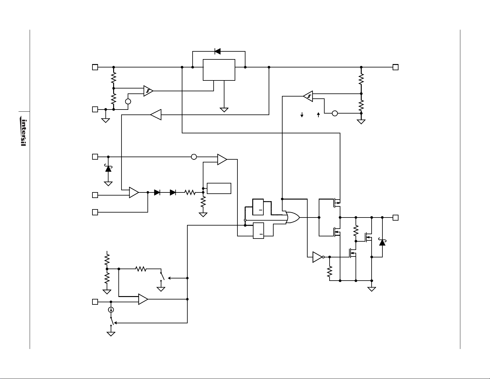
Functional Block Diagram
www.BDTIC.com/Intersil
V
DD
3
GND
CS
FB
COMP
ERROR
AMPLIFIER
VREF
START/STOP
UV COMPARATOR
+
-
+
-
2.5V
+
-
A
A = 0.5
VF TOTAL = 1.15V
DD
OKV
ENABLE
+
-
100mV
2R
COMPARATOR
R
V
REF
5.00V
PWM
+
-
1.1V
CLAMP
ONLY
ISL8841A/
ISL8844A/
ISL8845A
Q
T
Q
SRQ
Q
RESET
DOMINANT
VREF FAULT
VREF
UV COMPARATOR
4.65V 4.80V
-
+
-
+
36k
VREF
ISL8840A, ISL8841A, ISL8842A, ISL8843A, ISL8844A, ISL8845A
OUT
100k
150k
RTCT
April 18, 2007
FN6320.3
2.9V
1.0V
OSCILLATOR
COMPARATOR
8.4mA
ON
<10ns
+
ON
CLOCK
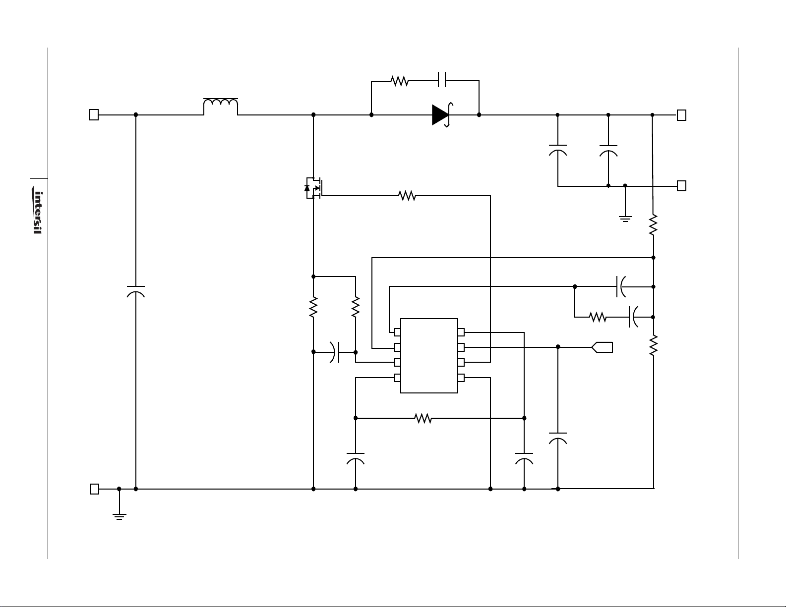
Typical Application - 48V Input Dual Output Flyback
www.BDTIC.com/Intersil
VIN+
4
R1
36V TO 75V
C1
C2
C3
R3
C4
CR6
Q1
C5
CR2
T1
C17
C6
R21
CR5
CR4
C19
+
R16
U2
C21
C15 C16
+
C22
+
C20
R17
R19
C14
R18
+3.3V
+
+1.8V
RETURN
ISL8840A, ISL8841A, ISL8842A, ISL8843A, ISL8844A, ISL8845A
R4
-
V
IN
R6
CR1
Q3
VR1
April 18, 2007
FN6320.3
C8
R26
R22
COMP
CS
FB
RTCT
R27
U4
VREF
ISL884xA
R10
V
DD
OUT
GND
R13
U3
C13
R15
R20
C12
C11
Typical Application - Boost Converter
www.BDTIC.com/Intersil
VIN+
R8
L1
CR1
C10
+VOUT
+
C2
C3
ISL8840A, ISL8841A, ISL8842A, ISL8843A, ISL8844A, ISL8845A
5
RETURN
R5
R6
C1
Q1
R1
C4
R2
R4
COMP
FB
CS
RTCT
U1
ISL884xA
VREF
VDD
OUT
GND
R7
VIN+
C9
C8
C7
VIN-
April 18, 2007
FN6320.3
R3
C5
C6

ISL8840A, ISL8841A, ISL8842A, ISL8843A, ISL8844A, ISL8845A
www.BDTIC.com/Intersil
Absolute Maximum Ratings Thermal Information
Supply Voltage, VDD . . . . . . . . . . . . . . . . . . . . . GND -0.3V to +30V
OUT . . . . . . . . . . . . . . . . . . . . . . . . . . . . . GND -0.3V to V
Signal Pins . . . . . . . . . . . . . . . . . . . . . . . . . . . . . GND -0.3V to 6.0V
Peak GATE Current. . . . . . . . . . . . . . . . . . . . . . . . . . . . . . . . . . . .1A
ESD Classification
Human Body Model (Per JESD22-A114C.01) . . . . . . . . . . .2000V
Machine Model (Per EIA/JESD22-A115-A) . . . . . . . . . . . . . .200V
Charged Device Model (Per JESD22-C191-A) . . . . . . . . . .1000V
DD
+ 0.3V
Thermal Resistance (Typical, Note 1) θ
SOIC Package . . . . . . . . . . . . . . . . . . . . . . . . . . . . . 100
MSOP Package . . . . . . . . . . . . . . . . . . . . . . . . . . . . 130
Maximum Junction Temperature . . . . . . . . . . . . . . .-55°C to +150°C
Maximum Storage Temperature Range. . . . . . . . . .-65°C to +150°C
Maximum Lead Temperature (Soldering 10s) . . . . . . . . . . . . +300°C
(SOIC, MSOP - Lead Tips Only)
Operating Conditions
Temperature Range
ISL884xAAxZ . . . . . . . . . . . . . . . . . . . . . . . . . . . .-40°C to +105°C
ISL884xAMxZ. . . . . . . . . . . . . . . . . . . . . . . . . . . .-55°C to +125°C
Supply Voltage Range (Typical, Note 2)
ISL884xA . . . . . . . . . . . . . . . . . . . . . . . . . . . . . . . . . . . . 9V to 30V
CAUTION: Stresses above those listed in “Absolute Maximum Ratings” may cause permanent damage to the device. This is a stress only rating and operation of the
device at these or any other conditions above those indicated in the operational sections of this specification is not implied.
+150°C max junction temperature is intended for short periods of time to prevent shortening the lifetime. Constantly operated at +150° C may shorten the life of the part.
NOTES:
is measured with the component mounted on a high effective thermal conductivity test board in free air. See Technical Brief TB379 for details.
1. θ
JA
2. All voltages are with respect to GND.
(°C/W)
JA
Electrical Specifications ISL884xAA - Recommended operating conditions unless otherwise noted. Refer to Block Diagram and
Typical Application schematic onpage 3 and page 4. V
(Note 3). Typical values are at T
PARAMETER TEST CONDITIONS MIN TYP MAX UNITS
UNDERVOLTAGE LOCKOUT
START Threshold (ISL8840A, ISL8841A) 6.5 7.0 7.5 V
START Threshold (ISL8843A, ISL8845A) 8.0 8.4 9.0 V
START Threshold (ISL8842A, ISL8844A) (Note 6) 13.3 14.3 15.3 V
STOP Threshold (ISL8840A, ISL8841A) 6.1 6.6 6.9 V
STOP Threshold (ISL8843A, ISL8845A) 7.3 7.6 8.0 V
STOP Threshold (ISL8842A, ISL8844A) 8.0 8.8 9.6 V
Hysteresis (ISL8840A, ISL8841A) - 0.4 - V
Hysteresis (ISL8843A, ISL8845A) - 0.8 - V
Hysteresis (ISL8842A, ISL8844A) - 5.4 - V
Startup Current, I
Operating Current, I
Operating Supply Current, I
REFERENCE VOLTAGE
Overall Accuracy Over line (V
Long Term Stability T
Current Limit, Sourcing -20 - - mA
Current Limit, Sinking 5--mA
CURRENT SENSE
Input Bias Current V
CS Offset Voltage V
COMP to PWM Comparator Offset Voltage V
DD
DD
D
VDD < START Threshold - 90 125 μA
(Note 4) - 2.9 4.0 mA
Includes 1nF GATE loading - 4.75 5.5 mA
temperature
= +125°C, 1000 hours (Note 5) - 5 - mV
A
= 1V -1.0 - 1.0 μA
CS
= 0V (Note 5) 95 100 105 mV
CS
= 0V (Note 5) 0.80 1.15 1.30 V
CS
= +25°C
A
= 12V to 30V), load,
DD
= 15V, RT = 10kΩ, CT = 3.3nF, TA = -40 to +105°C
DD
4.925 5.000 5.050 V
6
FN6320.3
April 18, 2007

ISL8840A, ISL8841A, ISL8842A, ISL8843A, ISL8844A, ISL8845A
www.BDTIC.com/Intersil
Electrical Specifications ISL884xAA - Recommended operating conditions unless otherwise noted. Refer to Block Diagram and
Typical Application schematic onpage 3 and page 4. V
(Note 3). Typical values are at T
PARAMETER TEST CONDITIONS MIN TYP MAX UNITS
Input Signal, Maximum 0.97 1.00 1.03 V
CS
= ΔV
DD
Gain, A
CS to OUT Delay -3555ns
ERROR AMPLIFIER
Open Loop Voltage Gain (Note 5) 60 90 - dB
Unity Gain Bandwidth (Note 5) 1.0 1.5 - MHz
Reference Voltage V
FB Input Bias Current V
COMP Sink Current V
COMP Source Current V
COMP VOH V
COMP VOL V
PSRR Frequency = 120Hz, V
OSCILLATOR
Frequency Accuracy Initial, T
Frequency Variation with V
Temperature Stability (Note 5) - - 5 %
Amplitude, Peak to Peak Static Test - 1.75 - V
RTCT Discharge Voltage (Valley Voltage) Static Test - 1.0 - V
Discharge Current RTCT = 2.0V 6.5 7.8 8.5 mA
OUTPUT
Gate VOH V
Gate VOL OUT to GND, I
Peak Output Current C
Rise Time C
Fall Time C
GATE VOL UVLO Clamp Voltage VDD = 5V, I
PWM
Maximum Duty Cycle
(ISL8840A, ISL8842A, ISL8843A)
Maximum Duty Cycle
(ISL8841A, ISL8844A, ISL8845A)
Minimum Duty Cycle COMP = GND - - 0 %
NOTES:
3. Specifications at -40°C and +105°C are guaranteed by +25°C test with margin limits.
4. This is the V
5. These parameters, although guaranteed, are not 100% tested in production.
6. Adjust V
/ΔVCS 0 < VCS < 910mV, VFB = 0V 2.5 3.0 3.5 V/V
COMP
= V
FB
= 0V -1.0 -0.2 1.0 μA
FB
COMP
COMP
= 2.3V 4.80 - VREF V
FB
= 2.7V 0.4 - 1.0 V
FB
30V (Note 5)
DD
current consumed when the device is active but not switching. Does not include gate drive current.
DD
above the start threshold and then lower to 15V.
TA= +25°C, (f
to OUT, I
DD
OUT
OUT
OUT
COMP = VREF 94.0 96.0 - %
COMP = VREF 47.0 48.0 - %
= +25°C (Continued)
A
COMP
= 1.5V, VFB = 2.7V 1.0 - - mA
= 1.5V, VFB = 2.3V -0.4 - - mA
= 12V to
DD
= +25°C 48 51 53 kHz
A
- f
30V
OUT
OUT
= 1nF (Note 5) - 1.0 - A
= 1nF (Note 5) - 20 40 ns
= 1nF (Note 5) - 20 40 ns
LOAD
)/f
10V
30V
= -200mA - 1.0 2.0 V
= 200mA - 1.0 2.0 V
= 1mA - - 1.2 V
= 15V, RT = 10kΩ, CT = 3.3nF, TA = -40 to +105°C
DD
2.475 2.500 2.530 V
60 80 - dB
-0.21.0%
7
FN6320.3
April 18, 2007

ISL8840A, ISL8841A, ISL8842A, ISL8843A, ISL8844A, ISL8845A
www.BDTIC.com/Intersil
Electrical Specifications ISL884xAM - Recommended operating conditions unless otherwise noted. Refer to Block Diagram and
Typical Applicati on schematic. V
are at T
PARAMETER TEST CONDITIONS MIN TYP MAX UNITS
UNDERVOLTAGE LOCKOUT
START Threshold (ISL8840A, ISL8841A) 6.5 7.0 7.5 V
START Threshold (ISL8843A, ISL8845A) 8.0 8.4 9.0 V
START Threshold (ISL8842A, ISL8844A) (Note 10) 13.3 14.3 15.3 V
STOP Threshold (ISL8840A, ISL8841A) 6.1 6.6 6.9 V
STOP Threshold (ISL8843A, ISL8845A) 7.3 7.6 8.0 V
STOP Threshold (ISL8842A, ISL8844A) 8.0 8.8 9.6 V
Hysteresis (ISL8840A, ISL8841A) - 0.4 - V
Hysteresis (ISL8843A, ISL8845A) - 0.8 - V
Hysteresis (ISL8842A, ISL8844A) - 5.4 - V
Startup Current, I
Operating Current, I
Operating Supply Current, I
REFERENCE VOLTAGE
Overall Accuracy Over line (V
Long Term Stability T
Current Limit, Sourcing -20 - - mA
Current Limit, Sinking 5--mA
CURRENT SENSE
Input Bias Current V
CS Offset Voltage V
COMP to PWM Comparator Offset Voltage V
Input Signal, Maximum 0.97 1.00 1.03 V
Gain, A
CS
CS to OUT Delay -3560ns
ERROR AMPLIFIER
Open Loop Voltage Gain (Note 9) 60 90 - dB
Unity Gain Bandwidth (Note 9) 1.0 1.5 - MHz
Reference Voltage V
FB Input Bias Current V
COMP Sink Current V
COMP Source Current V
COMP VOH V
COMP VOL V
PSRR Frequency = 120Hz, V
OSCILLATOR
Frequency Accuracy Initial, T
Frequency Variation with V
Temperature Stability (Note 9) - - 5 %
= ΔV
DD
DD
D
/ΔVCS 0 < VCS < 910mV, VFB = 0V 2.5 3.0 3.5 V/V
COMP
DD
= +25°C
A
VDD < START Threshold - 90 125 μA
(Note 8) - 2.9 4.0 mA
Includes 1nF GATE loading - 4.75 5.5 mA
temperature
= +125°C, 1000 hours (Note 9) - 5 - mV
A
= 1V -1.0 - 1.0 μA
CS
= 0V (Note 9) 95 100 105 mV
CS
= 0V (Note 9) 0.80 1.15 1.30 V
CS
= V
FB
= 0V -1.0 -0.2 1.0 μA
FB
COMP
COMP
= 2.3V 4.80 - VREF V
FB
= 2.7V 0.4 - 1.0 V
FB
30V (Note 9)
TA = +25°C, (f
= 15V , R T = 10kΩ, CT = 3.3nF , TA = -55 to +125°C (Note 7), Typical values
DD
= 12V to 30V), load,
DD
COMP
= 1.5V, VFB = 2.7V 1.0 - - mA
= 1.5V, VFB = 2.3V -0.4 - - mA
= 12V to
DD
= +25°C 485153kHz
A
- f
10V
)/f
30V
30V
4.900 5.000 5.050 V
2.460 2.500 2.535 V
60 80 - dB
-0.21.0%
8
FN6320.3
April 18, 2007

ISL8840A, ISL8841A, ISL8842A, ISL8843A, ISL8844A, ISL8845A
www.BDTIC.com/Intersil
Electrical Specifications ISL884xAM - Recommended operating conditions unless otherwise noted. Refer to Block Diagram and
Typical Applicati on schematic. V
are at T
PARAMETER TEST CONDITIONS MIN TYP MAX UNITS
Amplitude, Peak to Peak Static Test - 1.75 - V
RTCT Discharge Voltage (Valley Voltage) Static Test - 1.0 - V
Discharge Current RTCT = 2.0V 6.2 8.0 8.5 mA
OUTPUT
Gate VOH V
Gate VOL OUT - GND, I
Peak Output Current C
Rise Time C
Fall Time C
GATE VOL UVLO Clamp Voltage V
PWM
Maximum Duty Cycle
(ISL8840A, ISL8842A, ISL8843A)
Maximum Duty Cycle
(ISL8841A, ISL8844A, ISL8845A)
Minimum Duty Cycle COMP = GND - - 0 %
NOTES:
7. Specifications at -55°C and +125°C are guaranteed by +25°C test with margin limits.
8. This is the V
9. These parameters, although guaranteed, are not 100% tested in production.
10. Adjust V
current consumed when the device is active but not switching. Does not include gate drive current.
DD
above the start threshold and then lower to 15V.
DD
= +25°C (Continued )
A
- OUT, I
DD
OUT
OUT
OUT
= 5V, I
DD
COMP = VREF 94.0 96.0 - %
COMP = VREF 47.0 48.0 - %
= 15V , R T = 10kΩ, CT = 3.3nF , TA = -55 to +125°C (Note 7), Typical values
DD
= -200mA - 1.0 2.0 V
OUT
= 200mA - 1.0 2.0 V
OUT
= 1nF (Note 9) - 1.0 - A
= 1nF (Note 9) - 20 40 ns
= 1nF (Note 9) - 20 40 ns
= 1mA - - 1.2 V
LOAD
Typical Performance Curves
1.01
1.00
0.99
NORMALIZED FREQUENCY
0.98
-60 -40 -20 0 20 40 60 80 100 120 140
TEMPERATURE (°C)
FIGURE 1. FREQUENCY vs TEMPERATURE FIGURE 2. REFERENCE VOLTAGE vs TEMPERATURE
1.001
1.000
0.999
0.998
0.997
NORMALIZED VREF
0.996
0.995
-60 -40 -20 0 20 40 60 80 100
TEMPERATURE (°C)
140120
9
FN6320.3
April 18, 2007

ISL8840A, ISL8841A, ISL8842A, ISL8843A, ISL8844A, ISL8845A
www.BDTIC.com/Intersil
Typical Performance Curves (Continued)
1.001
3
10
1.000
0.998
0.997
NORMALIZED EA REFERENCE
0.996
-60 -40 -20 0 20 40 60 80 100 120 140
TEMPERATURE (°C)
FIGURE 3. EA REFERENCE vs TEMPERATURE
Pin Descriptions
RTCT - This is the oscillator timing control pin. The
operational frequency and maximum duty cycle are set by
connecting a resistor, RT, between VREF and this pin and a
timing capacitor, CT, from this pin to GND. The oscillator
produces a sawtooth waveform with a programmable
frequency range up to 2.0MHz. The charge time, t
discharge time, t
, the switching frequency, f, and the
D
maximum duty cycle, Dmax, can be approximated from the
following equations:
tC0.533 RT CT⋅⋅≈
t
RT– CT In
D
f 1t
Dt
C
⋅⋅≈
+()⁄=
CtD
f⋅=
0.008 RT 3.83–⋅
⎛
---------------------------------------------
⎝
0.008 RT 1.71–⋅
⎞
⎠
The formulae have increased error at higher frequencies due
to propagation delays. Figure 4 may be used as a guideline
in selecting the capacitor and resistor values required for a
given frequency.
COMP - COMP is the output of the error amplifier and the
input of the PWM comparator. The control loop frequency
compensation network is connected between the COMP and
FB pins.
FB - The output voltage feedback is connected to the
inverting input of the error amplifier through this pin. The
non-inverting input of the error amplifier is internally tied to a
reference voltage.
CS - This is the current sense input to the PWM comparator.
The range of the input signal is nominally 0V to 1.0V and has
an internal offset of 100mV.
GND - GND is the power and small signal reference ground
for all functions.
, the
C
(EQ. 1)
(EQ. 2)
(EQ. 3)
(EQ. 4)
100
10
FREQUENCY (Hz)
1
1 10 100
FIGURE 4. RESISTANCE FOR CT CAPACITOR VALUES GIVEN
RT (kΩ)
100pF
220pF
330pF
470pF
1.0nF
2.2nF
3.3nF
4.7nF
6.8nF
OUT - This is the drive output to the power switching device.
It is a high current output capable of driving the gate of a
power MOSFET with peak currents of 1.0A. This GATE
output is actively held low when V
is below the UVLO
DD
threshold.
V
- VDD is the power connection for the device. The total
DD
supply current will depend on the load applied to OUT. Total
I
current is the sum of the operating current and the
DD
average output current. Knowing the operating frequency, f,
and the MOSFET gate charge, Qg, the average output
current can be calculated from:
I
OUT
Qg f×=
To optimize noise immunity, bypass V
ceramic capacitor as close to the V
DD
to GND with a
DD
and GND pins as
(EQ. 5)
possible.
VREF - The 5.00V reference voltage output. +1.0/-1.5%
tolerance over line, load and operating temperature. Bypass
to GND with a 0.1μF to 3.3μF capacitor to filter this output as
needed.
Functional Description
Features
The ISL884xA current mode PWM makes an ideal choice for
low-cost flyback and forward topology applications. With its
greatly improved performance over industry standard parts,
it is the obvious choice for new designs or existing designs
which require updating.
Oscillator
The ISL884xA has a sawtooth oscillator with a
programmable frequency range to 2MHz, which can be
programmed with a resistor from VREF and a capacitor to
GND on the RTCT pin. (Please refer to Figure 4 for the
resistor and capacitance required for a given frequency.)
10
FN6320.3
April 18, 2007

ISL8840A, ISL8841A, ISL8842A, ISL8843A, ISL8844A, ISL8845A
www.BDTIC.com/Intersil
Soft-Start Operation
Soft-start must be implemented externally. One method,
illustrated below, clamps the voltage on COMP.
D1 R1
C1
FIGURE 5. SOFT-START
VREF
COMP
Q1
GND
ISL884xA
The COMP pin is clamped to the voltage on capacitor C1
plus a base-emitter junction by transistor Q1. C1 is charged
from VREF through resistor R1 and the base current of Q1.
At power-up C1 is fully discharged, COMP is at ~0.7V, and
the duty cycle is zero. As C1 charges, the voltage on COMP
increases, and the duty cycle increases in proportion to the
voltage on C1. When COMP reaches the steady state
operating point, the control loop takes over and soft start is
complete. C1 continues to charge up to VREF and no longer
affects COMP. During power down, diode D1 quickly
discharges C1 so that the soft start circuit is properly
initialized prior to the next power on sequence.
Gate Drive
The ISL884xA is capable of sourcing and sinking 1A peak
current. To limit the peak current through the IC, an optional
external resistor may be placed between the totem-pole
output of the IC (OUT pin) and the gate of the MOSFET. This
small series resistor also damps any oscillations caused by
the resonant tank of the parasitic inductances in the traces of
the board and the FET’s input capacitance.
From the small signal current-mode model [1] it can be
shown that the naturally-sampled modulator gain, Fm,
without slope compensation, is in Equation 6.
1
------------------- -
Fm
=
SnTsw
(EQ. 6)
where Sn is the slope of the sawtooth signal and Tsw is the
duration of the half-cycle. When an external ramp is added,
the modulator gain becomes:
1
---------------------------------------
==
Fm
Sn Se+()Tsw
1
----------------------------
SnTsw
m
c
(EQ. 7)
where Se is slope of the external ramp and
Se
m
-------
1
+=
c
Sn
(EQ. 8)
The criteria for determining the correct amount of external
ramp can be determined by appropriately setting the
damping factor of the double-pole located at the switching
frequency. The double-pole will be critically damped if the
Q-factor is set to 1, over-damped for Q < 1, and
under-damped for Q > 1. An under-damped condition may
result in current loop instability.
-------------------------------------------------
=
Q
π m
c
1
1D–()0.5–()
(EQ. 9)
where D is the percent of on time during a switching cycle.
Setting Q = 1 and solving for Se yields
S
eSn
1
⎛⎞
⎛⎞
-- -
=
⎝⎠
⎝⎠
π
1
-------------
0.5+
1D–
1–
(EQ. 10)
Since Sn and Se are the on time slopes of the current ramp
and the external ramp, respectively , they can be multiplied
by t
to obtain the voltage change that occurs during tON.
ON
V
eVn
1
⎛⎞
⎛⎞
-- -
=
⎝⎠
⎝⎠
π
1
-------------
0.5+
1D–
1–
(EQ. 11)
Slope Compensation
For applications where the maximum duty cycle is less than
50%, slope compensation may be used to improve noise
immunity, particularly at lighter loads. The amount of slope
compensation required for noise immunity is determined
empirically, but is generally about 10% of the full scale
current feedback signal. For applications where the duty
cycle is greater than 50%, slope compensation is required to
prevent instability.
where Vn is the change in the current feedback signal (ΔI)
during the on time and Ve is the voltage that must be added
by the external ramp.
For a flyback converter, Vn can be solved for in terms of
input voltage, current transducer components, and primary
inductance, yielding
DT⋅
SWVINRCS
----------------------------------------------------
V
= V
e
Slope compensation may be accomplished by summing an
external ramp with the current feedback signal or by
subtracting the external ramp from the voltage feedback
error signal. Adding the external ramp to the current
feedback signal is the more popular method.
where R
frequency, L
is the current sense resistor, f
CS
p
input voltage, and D is the maximum duty cycle.
11
⋅⋅
L
p
1
⎛⎞
⎛⎞
-- -
⎝⎠
⎝⎠
π
1
-------------
0.5+
1D–
1–
is the switching
sw
(EQ. 12)
is the primary inductance, VIN is the minimum
FN6320.3
April 18, 2007

ISL8840A, ISL8841A, ISL8842A, ISL8843A, ISL8844A, ISL8845A
www.BDTIC.com/Intersil
The current sense signal at the end of the ON time for CCM
operation is:
NSRCS⋅
------------------------
V
= V (EQ. 13)
CS
where V
L
is the secondary winding inductance, and IO is the output
s
N
P
is the voltage across the current sense resistor,
CS
1D–()VOf⋅⋅
⎛⎞
--------------------------------------------
I
+
⎜⎟
O
⎝⎠
2L
sw
s
current at current limit. Equation 13 assumes the voltage
drop across the output rectifier is negligible.
Since the peak current limit threshold is 1.00V, the total
current feedback signal plus the external ramp voltage must
sum to this value when the output load is at the current limit
threshold.
+ 1=
V
eVCS
(EQ. 14)
Substituting Equations 12 and 13 into Equation 14 and
solving for R
---------------------------------------------------------------------------------------------------------------------------------------------------- -
R
=
CS
Df
-------------------------------
yields
CS
⋅⋅
swVIN
L
p
1
1
-- -
0.5+
⎛⎞
π
⎜⎟
----------------- -
⋅
⎜⎟
1D–
⎝⎠
N
s
-------
1–
N
p
1D–()VOf
⎛⎞
I
+
⋅+
⎜⎟
O
⎝⎠
⋅⋅
2L
sw
s
(EQ. 15)
--------------------------------------------
Adding slope compensation is accomplished in the
ISL884xA using an external buffer transistor and the RTCT
signal. A typical application sums the buffered RTCT signal
with the current sense feedback and applies the result to the
CS pin as shown in Figure 6.
VREF
R9
R6
C4
FIGURE 6. SLOPE COMPENSATION
ISL8843
CS
RTCT
Assuming the designer has selected values for the RC filter
(R
and C4) placed on the CS pin, the value of R9 required
6
to add the appropriate external ramp can be found by
superposition.
2.05D R6⋅
----------------------------
V
= V
e
R
6R9
+
(EQ. 16)
The factor of 2.05 in Equation 16 arises from the peak
amplitude of the sawtooth waveform on RTCT minus a
base-emitter junction drop. That voltage multiplied by the
maximum duty cycle is the voltage source for the slope
compensation. Rearranging to solve for R
2.05D Ve–()R6⋅
----------------------------------------------
R
= Ω
9
V
e
yields:
9
(EQ. 17)
The value of RCS determined in Equation 15 must be
rescaled so that the current sense signal presented at the
CS pin is that predicted by Equation 13. The divider created
by R
and R9 makes this necessary.
6
R6R9+
CS
---------------------
R
9
⋅=
R
CS
(EQ. 18)
R′
12
FN6320.3
April 18, 2007

ISL8840A, ISL8841A, ISL8842A, ISL8843A, ISL8844A, ISL8845A
www.BDTIC.com/Intersil
Example:
VIN = 12V
VO = 48V
Ls = 800μH
Ns/Np = 10
Lp = 8.0μH
IO = 200mA
Switching Frequency, fsw = 200kHz
Duty Cycle, D = 28.6%
R6 = 499Ω
Solve for the current sense resistor, RCS, using Equation 15.
RCS = 295mΩ
Determine the amount of voltage, Ve, that must be added to
the current feedback signal using Equation 12.
Ve = 92.4mV
Using Equation 17, solve for the summing resistor, R
CT to CS.
, from
9
Fault Conditions
A Fault condition occurs if VREF falls below 4.65V. When a
Fault is detected OUT is disabled. When VREF exceeds
4.80V, the Fault condition clears, and OUT is enabled.
Ground Plane Requirements
Careful layout is essential for satisfactory operation of the
device. A good ground plane must be employed. A unique
section of the ground plane must be designated for high di/dt
currents associated with the output stage. V
bypassed directly to GND with good high frequency
capacitors.
should be
DD
References
[1] Ridley , R., “A New Continuous-T ime Model for Current
Mode Control”, IEEE Transactions on Power
Electronics, Vol. 6, No. 2, April 1991.
R
= 2.67kΩ
9
Determine the new value of R
R’CS = 350mΩ
Additional slope compensation may be considered for
design margin. The above discussion determines the
minimum external ramp that is required. The buffer transistor
used to create the external ramp from RTCT should have a
sufficiently high gain (>200) so as to minimize the required
base current. Whatever base current is required reduces the
charging current into RTCT and will reduce the oscillator
frequency.
(R’CS) using Equation 18.
CS
13
FN6320.3
April 18, 2007

ISL8840A, ISL8841A, ISL8842A, ISL8843A, ISL8844A, ISL8845A
www.BDTIC.com/Intersil
Small Outline Plastic Packages (SOIC)
N
INDEX
AREA
123
-A-
E
-B-
SEATING PLANE
D
A
-C-
0.25(0.010) BM M
H
L
h x 45°
α
e
B
0.25(0.010) C AM BS
NOTES:
1. Symbols are defined in the “MO Series Symbol List” in Section 2.2 of
Publication Number 95.
2. Dimensioning and tolerancing per ANSI Y14.5M-1982.
3. Dimension “D” does not include mold flash, protrusions or gate burrs.
Mold flash, protrusion and gate burrs shall not exceed 0.15mm (0.006
inch) per side.
4. Dimension “E” does not include interlead flash or protrusions. Interlead flash and protrusions shall not exceed 0.25mm (0.010 inch) per
side.
5. The chamfer on the body is optional. If it is not present, a visual index
feature must be located within the crosshatched area.
6. “L” is the length of terminal for soldering to a substrate.
7. “N” is the number of terminal positions.
8. Terminal numbers are shown for reference only.
9. The lead width “B”, as measured 0.36mm (0.014 inch) or greater
above the seating plane, shall not exceed a maximum value of
0.61mm (0.024 inch).
10. Controlling dimension: MILLIMETER. Converted inch dimensions
are not necessarily exact.
M
A1
C
0.10(0.004)
M8.15 (JEDEC MS-012-AA ISSUE C)
8 LEAD NARROW BODY SMALL OUTLINE PLASTIC PACKAGE
INCHES MILLIMETERS
SYMBOL
A 0.0532 0.0688 1.35 1.75 -
A1 0.0040 0.0098 0.10 0.25 -
B 0.013 0.020 0.33 0.51 9
C 0.0075 0.0098 0.19 0.25 -
D 0.1890 0.1968 4.80 5.00 3
E 0.1497 0.1574 3.80 4.00 4
e 0.050 BSC 1.27 BSC -
H 0.2284 0.2440 5.80 6.20 -
h 0.0099 0.0196 0.25 0.50 5
L 0.016 0.050 0.40 1.27 6
N8 87
α
0° 8° 0° 8° -
NOTESMIN MAX MIN MAX
Rev. 1 6/05
14
FN6320.3
April 18, 2007

ISL8840A, ISL8841A, ISL8842A, ISL8843A, ISL8844A, ISL8845A
www.BDTIC.com/Intersil
Mini Small Outline Plastic Packages (MSOP)
N
EE1
INDEX
AREA
AA1A2
-H-
SIDE VIEW
12
TOP VIEW
b
e
D
NOTES:
1. These package dimensions are within allowable dimensions of
JEDEC MO-187BA.
2. Dimensioning and tolerancing per ANSI Y14.5M-1994.
3. Dimension “D” does not include mold flash, protrusions or gate
burrs and are measured at Datum Plane. Mold flash, protrusion
and gate burrs shall not exceed 0.15mm (0.006 inch) per side.
4. Dimension “E1” does not include interlead flash or protrusions
and are measured at Datum Plane. Interlead flash and
protrusions shall not exceed 0.15mm (0.006 inch) per side.
5. Formed leads shall be planar with respect to one another within
0.10mm (0.004) at seating Plane.
6. “L” is the length of terminal for soldering to a substrate.
7. “N” is the number of terminal positions.
8. Terminal numbers are shown for reference only.
9. Dimension “b” does not include dambar protrusion. Allowable
dambar protrusion shall be 0.08mm (0.003 inch) total in excess
of “b” dimension at maximum material condition. Minimum space
between protrusion and adjacent lead is 0.07mm (0.0027 inch).
- H -
-A -
.
10. Datums and to be determined at Datum plane
11. Controlling dimension: MILLIMETER. Converted inch dimensions are for reference only.
-B-
0.20 (0.008) A
GAUGE
PLANE
SEATING
PLANE
0.10 (0.004) C
-A-
0.20 (0.008) C
- B -
0.25
(0.010)
-C-
SEATING
PLANE
a
0.20 (0.008) C
- H -
B
4X θ
C
D
4X θ
L1
C
C
L
E
1
END VIEW
R1
R
L
-B-
M8.118 (JEDEC MO-187AA)
8 LEAD MINI SMALL OUTLINE PLASTIC PACKAGE
INCHES MILLIMETERS
SYMBOL
A 0.037 0.043 0.94 1.10 A1 0.002 0.006 0.05 0.15 A2 0.030 0.037 0.75 0.95 -
b 0.010 0.014 0.25 0.36 9
c 0.004 0.008 0.09 0.20 -
D 0.116 0.120 2.95 3.05 3
E1 0.116 0.120 2.95 3.05 4
e 0.026 BSC 0.65 BSC -
E 0.187 0.199 4.75 5.05 -
L 0.016 0.028 0.40 0.70 6
L1 0.037 REF 0.95 REF -
N8 87
R 0.003 - 0.07 - R1 0.003 - 0.07 - -
0 5
α
o
o
0
15
o
o
6
o
5
o
0
15
o
o
6
Rev. 2 01/03
NOTESMIN MAX MIN MAX
-
-
All Intersil U.S. products are manufactured, assembled and tested utilizing ISO9000 quality systems.
Intersil Corporation’s quality certifications can be viewed at www.intersil.com/design/quality
Intersil products are sold by description only. Intersil Corporation reserves the right to make changes in circuit design, software and/or specifications at any time without
notice. Accordingly, the reader is cautioned to verify that data sheets are current before placing orders. Information furnished by Intersil is believed to be accurate and
reliable. However, no responsibility is assumed by Intersil or its subsidiaries for its use; nor for any infringements of patents or other rights of third parties which may result
from its use. No license is granted by implic atio n or other wise u nde r any p a tent or patent rights of Intersil or its subsidiaries.
For information regarding Intersil Corporation and its products, see www.intersil.com
15
FN6320.3
April 18, 2007
 Loading...