

Page 1

Table of Contents
1 DETAILED DESCRIPTION . . . . . . . . . . . . . . . . . . . . . . . . . . . . . . . . . . . . . . . . . . . . . . .1
1.1 Speech/Sound Quality . . . . . . . . . . . . . . . . . . . . . . . . . . . . . . . . . . . . . . . . . . . . . . . 1
1.2 Duration . . . . . . . . . . . . . . . . . . . . . . . . . . . . . . . . . . . . . . . . . . . . . . . . . . . . . . . . . . . 1
1.3 Flash Storage . . . . . . . . . . . . . . . . . . . . . . . . . . . . . . . . . . . . . . . . . . . . . . . . . . . . . . . 1
1.4 Microcontroller Interface . . . . . . . . . . . . . . . . . . . . . . . . . . . . . . . . . . . . . . . . . . . . . 1
1.5 Programming . . . . . . . . . . . . . . . . . . . . . . . . . . . . . . . . . . . . . . . . . . . . . . . . . . . . . . . 1
2 PIN DESCRIPTIONS . . . . . . . . . . . . . . . . . . . . . . . . . . . . . . . . . . . . . . . . . . . . . . . . . . .2
2.1 Digital I/O Pins . . . . . . . . . . . . . . . . . . . . . . . . . . . . . . . . . . . . . . . . . . . . . . . . . . . . . .2
2.2 Analog I/O Pins . . . . . . . . . . . . . . . . . . . . . . . . . . . . . . . . . . . . . . . . . . . . . . . . . . . . . 3
2.3 Power and Ground Pins . . . . . . . . . . . . . . . . . . . . . . . . . . . . . . . . . . . . . . . . . . . . . . 6
3 INTERNAL FUNCTIONAL BLOCKS . . . . . . . . . . . . . . . . . . . . . . . . . . . . . . . . . . . . . . . .7
4 SERIAL PERIPHERAL INTERFACE (SPI) DESCRIPTION . . . . . . . . . . . . . . . . . . . . . . . .13
4.1 Message Cueing . . . . . . . . . . . . . . . . . . . . . . . . . . . . . . . . . . . . . . . . . . . . . . . . . . . 13
4.2 Power-Up Sequence . . . . . . . . . . . . . . . . . . . . . . . . . . . . . . . . . . . . . . . . . . . . . . . . 14
4.3 SPI Port . . . . . . . . . . . . . . . . . . . . . . . . . . . . . . . . . . . . . . . . . . . . . . . . . . . . . . . . . . . 15
4.4 SPI Control Register . . . . . . . . . . . . . . . . . . . . . . . . . . . . . . . . . . . . . . . . . . . . . . . . . 15
5 OPERATIONAL MODES DESCRIPTION . . . . . . . . . . . . . . . . . . . . . . . . . . . . . . . . . . .18
5.1 Feed Through Mode . . . . . . . . . . . . . . . . . . . . . . . . . . . . . . . . . . . . . . . . . . . . . . . . 18
5.2 Call Record . . . . . . . . . . . . . . . . . . . . . . . . . . . . . . . . . . . . . . . . . . . . . . . . . . . . . . . 20
5.3 Memo Record . . . . . . . . . . . . . . . . . . . . . . . . . . . . . . . . . . . . . . . . . . . . . . . . . . . . . 21
5.4 Memo and Call Record Playback . . . . . . . . . . . . . . . . . . . . . . . . . . . . . . . . . . . . 21
6 TIMING DIAGRAMS . . . . . . . . . . . . . . . . . . . . . . . . . . . . . . . . . . . . . . . . . . . . . . . . .31
7 DEVICE PHYSICAL DIMENSIONS . . . . . . . . . . . . . . . . . . . . . . . . . . . . . . . . . . . . . . .33
8 ORDERING INFORMATION . . . . . . . . . . . . . . . . . . . . . . . . . . . . . . . . . . . . . . . . . . .39
ISD
iii
Page 2

ISD5008 Product
iv
Voice Solutions in Silicon™
Page 3
®
A Winbond Company
ISD5008
Single-Chip Voice Record/Playback Device
4-, 5-, 6-, and 8-Minute Durations
Preliminary Datasheet
ISD5008 PRODUCT SUMMARY
The ISD5008 ChipCorder product is a fully-integrated, single-chip solution which provides
seamless integration of enhanced voice record
and playback features for digital cellular phones
(GSM, CDMA, TDMA, PDC, and PHS), automotive
communications, GPS/navigation systems, and
portable communication products. This lowpower, 3-volt product enables customers to
quickly and easily integrate 4 to 8 minutes of
voice storage features such as one-way and
two-way (full duplex) call record, voice memo
record, and call screening/answering machine
functionality.
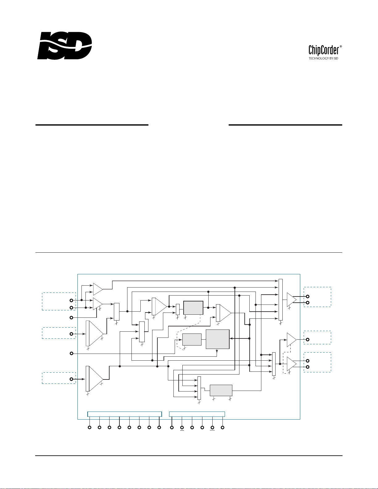
Figure 4-1: ISD5008 Block Diagram
MICROPHONE
MIC+
MIC–
AGCCAP
CAR KIT
AUX IN
XCLK
CHIP SET
ANA IN
6dB
AGC
1.0/1.4/2.0/2.8
AUX IN
AMP
AXG0
()
AXG1
2
.63/.88/1.3/1.8
ANA IN
AMP
AIG0
2
()
AIG1
INPUT
SOURCE
MUX
1
(AGPD)
1
(AXPD)
1
(AIPD)
Power Conditioning Device Control
1
(INS0)
SUM1
SUMMING
AMP
SUM1
MUX
2
S1S0
()
S1S1
2
S1M0
()
S1M1
FILTER
MUX
(FLS0)
Like other ChipCorder products, the ISD5008 integrates the sampling clock, anti-aliasing and
smoothing filters, and the multi-level storage array on a single-chip. For enhanced voice features, the ISD5008 eliminates external circuitry by
also integrating automatic gain control (AGC), a
power amplifier/speaker driver, volume control,
summing amplifiers, analog switches, and a car
kit interface. Input level adjustable amplifiers are
also included, providing a flexible interface for
multiple applications.
Low Pass
1
Internal
2
ANA IN
SUM 2
SUM 1
()
Filter
1
(FLPD)
Clock
FLD0
()
FLD1
INP
VLS0
VLS1
2
VOL
MUX
SUM2
SUMMING AMP
S2M0
2
()
S2M1
Multilevel
Storage
Array
Volume
Control
3
VOL0
VOL1
()
VOL2
1
FTHRU
VOL
FILTO
SUM1
SUM2
()
OUTPUT
(VLPD)
INP
AOS0
AOS1
AOS2
MUX
()
2
OPS0
OPS1
ANA OUT
MUX
(AOPD)
3
()
1
2
OPA0
OPA1
CHIP SET
ANA OUT+
ANA OUT–
CAR KIT
AUX OUT
SPEAKER
SP+
SP–
VCCA VSSA VSSA VSSA VSSD VSSD VCCD VCCD
SCLK SS MOSI MISO INT RAC
JUNE 1999
ISD · 2727 North First Street, San Jose, CA 95134 · TEL: 408/943-6666 · FAX: 408/544-1787 · http://www.isd.com
Page 4

ISD5008 Product
Duration/sample rate selection is accomplished
via software, allowing customers to optimize
quality and duration for various features within
the same end product.
The ISD5008 device is designed for use in a microprocessor- or microcontroller-based system. Address, control, and duration selection are
accomplished through a Serial Peripheral Interface (SPI) or Microwire Serial Interface to minimize pin count.
Recordings are stored in on-chip nonvolatile
memory cells, providing zero-power message
storage. This unique, single-chip solution is made
possible through ISD’s patented multilevel storage technology. Voice and audio signals are
stored directly into solid-state memory in their
natural, uncompressed form, providing superior
quality voice and music reproduction.
ISD5008 FEATURES
Enhanced Voice Features
¥ One or two-way (full duplex) conversation
record (record signal summation)
¥ One- or two-way (full duplex) message
playback (while on a call)
¥ Voice memo record and playback
¥ Private call screening
¥ In-terminal answering machine
¥ Personalized outgoing message (given caller
ID information from host chip set)
¥ Private call announce while on call (given
CIDCW information from host chip set)
Easy-to-Use and Control
¥ No compression algorithm development
required
¥ User-controllable sample rates of 8.0 kHz,
6.4 kHz, 5.3 kHz, or 4.0 kHz providing up to
8 minutes of voice storage.
Fully-Integrated Solution
¥ Single-chip voice record/playback solution
¥ Integrated sampling clock, anti-aliasing and
smoothing filters, and multi-level storage
array
¥ Integrated analog features such as
automatic gain control (AGC), audio gating
switches, speaker driver (23mW with 8 ohm
load), summing amplifiers, volume control,
and an AUX IN/AUX OUT interface (e.g., for
car kits).
Low-Power Consumption
¥ Single +3 volt supply
¥ Operating current:
I
CC Play
I
CC Rec
I
CC Feedthru
¥ Standby current:
I
SB
¥ Power consumption controlled by SPI or
Microwire control register
= 15 mA (typical)
= 25 mA (typical)
= 12 mA (typical)
= 1 µA
¥ Microcontroller SPI or Microwire™ Serial
Interface
¥ Fully addressable to handle multiple
messages in 1200 rows
High Quality Solution
¥ High quality voice and music reproduction
¥ ISD’s standard 100-year message retention
(typical)
¥ 100,000 record cycles (typical)
Options
¥ Available in die form, PDIP, SOIC, TSOP, and
chip scale packaging (CSP)
¥ Industrial temperature (–40˚C to +85˚C)
versions available
¥ Most stages can be individually powered
down for minimum power consumption
ii
Voice Solutions in Silicon
™
Page 5
ISD5008 Product
1 DETAILED DESCRIPTION
1.1 SPEECH/SOUND QUALITY
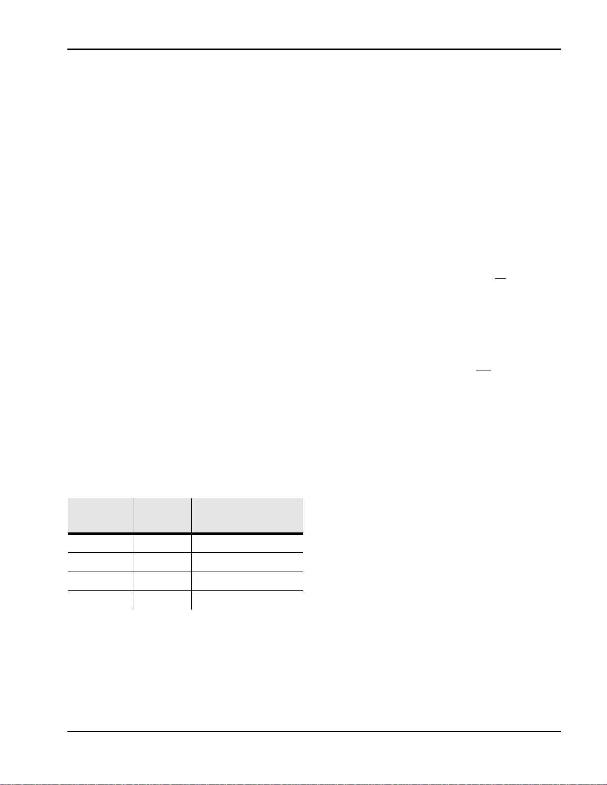
The ISD5008 ChipCorder product can be configured via software to operate at 4.0, 5.3, 6.4,
and 8.0 kHz sampling frequencies, allowing the
user a choice of speech quality options. Increasing the duration decreases the sampling
frequency and bandwidth, which affects
sound quality. Table 1 compares filter pass
band and product durations.
The speech samples are stored directly into onchip nonvolatile memory without the digitization and compression associated with other
solutions. Direct analog storage provides a
natural sounding reproduction of voice, music, tones, and sound effects not available
with most solid-state solutions.
1.2 DURATION
To meet end system requirements, the ISD5008
device is a single-chip solution which provides
from 4 to 8 minutes of voice record and playback, depending on the sample rates defined by customer software.
Table 1: Input Sample Rate to Duration
Input Sample
Rate (kHz)
8.0 4.0 3.4
6.4 5.0 2.7
5.3
Duration
(Minutes)
6.0
Typical Filter P ass Band
(kHz)
2.3
1.3 FLASH STORAGE
One of the benefits of ISD’s ChipCorder technology is the use of on-chip nonvolatile memory,
which provides zero-power message storage.
The message is retained for up to 100 years
(typically) without power. In addition, the device can be re-recorded over 100,000 times
(typically).
1.4 MICROCONTROLLER INTERFACE
A four-wire (SCLK, MOSI, MISO, SS
face is provided for ISD5008 control, addressing functions, and sample rate selection. The
ISD5008 is configured to operate as a peripheral slave device with a microcontrollerbased SPI bus interface. Read/Write access to
all the internal registers occurs through this SPI
interface. An interrupt signal (INT
read-only Status Register are provided for
handshake purposes.
) SPI inter-
) and internal
1.5 PROGRAMMING
The ISD5008 series is also ideal for playbackonly applications, where single or multiple
message Playback is controlled through the
SPI port. Once the desired message configuration is created, duplicates can easily be generated via an ISD or third-party programmers.
For more information on available application
tools and programmers please see the ISD
web site at www.isd.com.
ISD
4.0
8.0
1.7
1
Page 6

ISD5008 Product
2 PIN DESCRIPTIONS
2.1 DIGITAL I/O PINS
SCLK (Serial Clock)
The SCLK is the clock input to the ISD5008.
Generated by the master microcontroller, the
SCLK synchronizes data transfers in and out of
the device through the MISO and MOSI lines.
Data is latched into the ISD5008 on the rising
edge of SCLK and shifted out on the falling
edge.
SS
This input, when LOW, will select the ISD5008
device.
MOSI (Master Out Slave In)
MOSI is the serial data input to the ISD5008 device. The master microcontroller places data
to be clocked into the ISD5008 device on the
MOSI line one-half cycle before the rising
edge of SCLK. Data is clocked into the device
LSB (Least Significant Bit) first.
(Slave Select)
OVF Flag
end of the ISD5008’s analog memory has
been reached during a record or playback
operation.
EOM Flag.
during playback, when an EOM is found.
There are eight possible EOM markers per row.
. The overflow flag indicates that the
The end of message flag is set only
RAC (Row Address Clock)
RAC is an open drain output pin that normally
marks the end of a row. At the 8 kHz sample
frequency, the duration of this period is
200 ms. There are 1,200 rows of memory in the
ISD5008 devices. RAC stays HIGH for 175 ms
and stays LOW for the remaining 25 ms before
it reaches the end of the row.
The RAC pin remains HIGH for 109.38 µsec and
stays LOW for 15.63 µsec under the Message
Cueing mode. See Table 15 AC Parameters
for RAC timing information at other sample
rates. When a record command is first initiated, the RAC pin remains HIGH for an extra T
period, to load sample and hold circuits
ACLO
internal to the device. The RAC pin can be
used for message management techniques.
R-
MISO (Master In Slave Out)
MISO is the serial data output of the ISD5008
device. Data is clocked out on the falling
edge of SCLK. This output goes into a high-impedance state when the device is not selected. Data is clocked out of the device LSB first.
INT
INT
is an open drain output pin. The ISD5008 interrupt pin goes LOW and stays LOW when an
Overflow (OVF) or End of Message (EOM)
marker is detected. Each operation that ends
in an EOM or OVF generates an interrupt, including the message cueing cycles. The interrupt is cleared the next time an SPI cycle is
completed. The interrupt status can be read
by a RINT instruction that will give one of the
two flags out the MISO line.
(Interrupt)
XCLK (External Clock Input)
The external clock input for the ISD5008 product has an internal pull-down device. Normally, the ISD5008 is operated at one of four
internal rates selected for its internal oscillator
by the Sample Rate Select bits. If greater precision is required, the device can be clocked
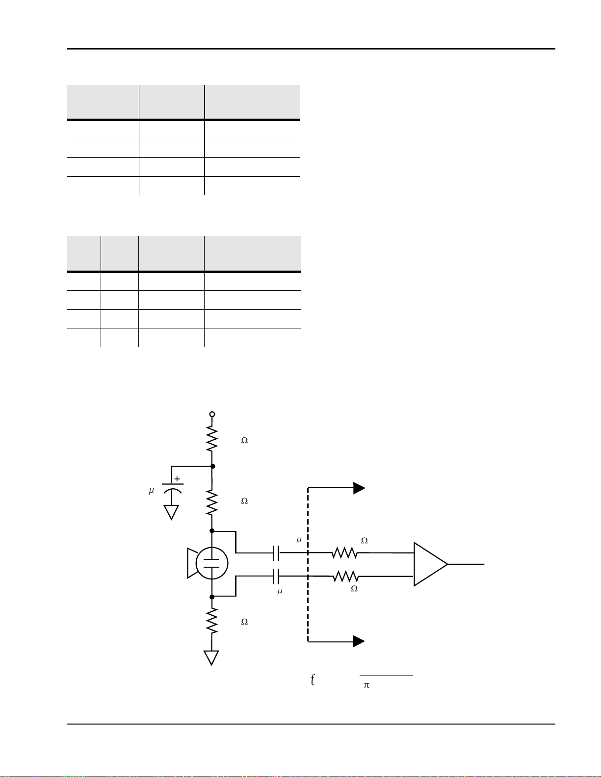
through the XCLK pin as described in Table 2 .
Because the antialiasing and smoothing filters
track the Sample Rate Select bits, one must,
for optimum performance, change the external clock
bits to one of the four values to properly set
the filters to the correct cutoff frequency as
described in Table 3. The duty cycle on the input clock is not critical, as the clock is immediately divided by two internally. If the XCLK is
not used, this input should be connected to
V
SSD
AND
the Sample Rate Configuration
.
2
Voice Solutions in Silicon
™
Page 7
ISD5008 Product
Table 2: External Clock Input Table
Duration
(Minutes)
4 8.0 1024
5 6.4 819.2
6 5.3 682.7
8 4.0 512
Sample Rate
(kHz)
Required Clock
(kHz)
Table 3: I nternal Clock Rate/Filter Edge
FLD1
FLD0
0 0 8 3.4
0 1 6.4 2.7
1 0 5.3 2.3
1 1 4 1.7
Sample Rate
(kHz)
Filter Pass Band
(kHz)
2.2 ANALOG I/O PINS
MIC+, MIC –(Microphone Input+/–)
The microphone input transfers the voice signal to the on-chip AGC preamplifier or directly to the ANA OUT MUX, depending on the
selected path. The direct path to the ANA
OUT MUX has a gain of 6 dB so a 208 mVp-p
signal across the differential microphone inputs would give 416 mVp-p across the ANA
OUT pins. The AGC circuit has a range of 45 dB
in order to deliver a nominal 694 mVp-p into
the storage array from a typical electret microphone output of 2 to 20 mVp-p. The input
impedance is typically 10 kΩ.
220 F
Electret
Microphone
WM-54B
Panasonic
VCC
Figure 1: Microphone Input
1.5 k
= 0.1 F
0.1
MIC+
F
MIC–
Ra = 10 k
10 k
1.5 k
1.5 k
C
COUP
Internal to the device
ISD
NOTE: CUTOFF=
2
RaC
1
COUP
3
Page 8
1.
2.
3.
4.
ISD5008 Product
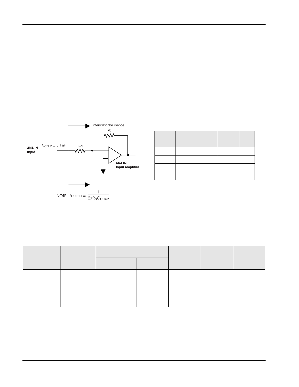
ANA IN (Analog Input)
The ANA IN pin is the analog input from the
telephone chip set. It can be switched (by the
SPI bus) to the speaker output, the array input
or to various other paths. This pin is designed to
accept a nominal 1.11 Vp-p when at its minimum gain (6 dB) setting. There is additional
gain available in 3 dB steps controlled from
the SPI bus, if required, up to 15 dB.
Figure 2: ANA IN Input Modes
Gain
Setting
Resistor Ratio
(Rb/Ra)
Gain
00 63.9/102 0.625 –4.1
01 77.9/88.1 0.88 –1.1
10 92.3/73.8 1.25 1.9
11 106/60 1.77 4.9
Table 4: ANA IN Amplifier Gain Settings
Setting
(1)
0TLP Input
(3)
V
PP
AIG1
6 dB 1.11 0 0 .625 .694 2.22
CFG0
AIG0
Gain
(2)
Array In/Out
V
PP
Speaker Out
Gain
(dB)
V
PP
2
(4)
9 dB .785 0 1 .883 .694 2.22
12 dB .555 1 0 1.250 .694 2.22
15 dB .393 1 1 1.767 .694 2.22
Gain from ANA IN to SP+/–
Gain from ANA IN to ARRAY IN
0TLP Input is the reference Transmission Level Point that is used for testing. This level is typically 3 dB below clipping.
Speaker Out gain set to 1.6 (High). (Differential)
4
Voice Solutions in Silicon
™
Page 9
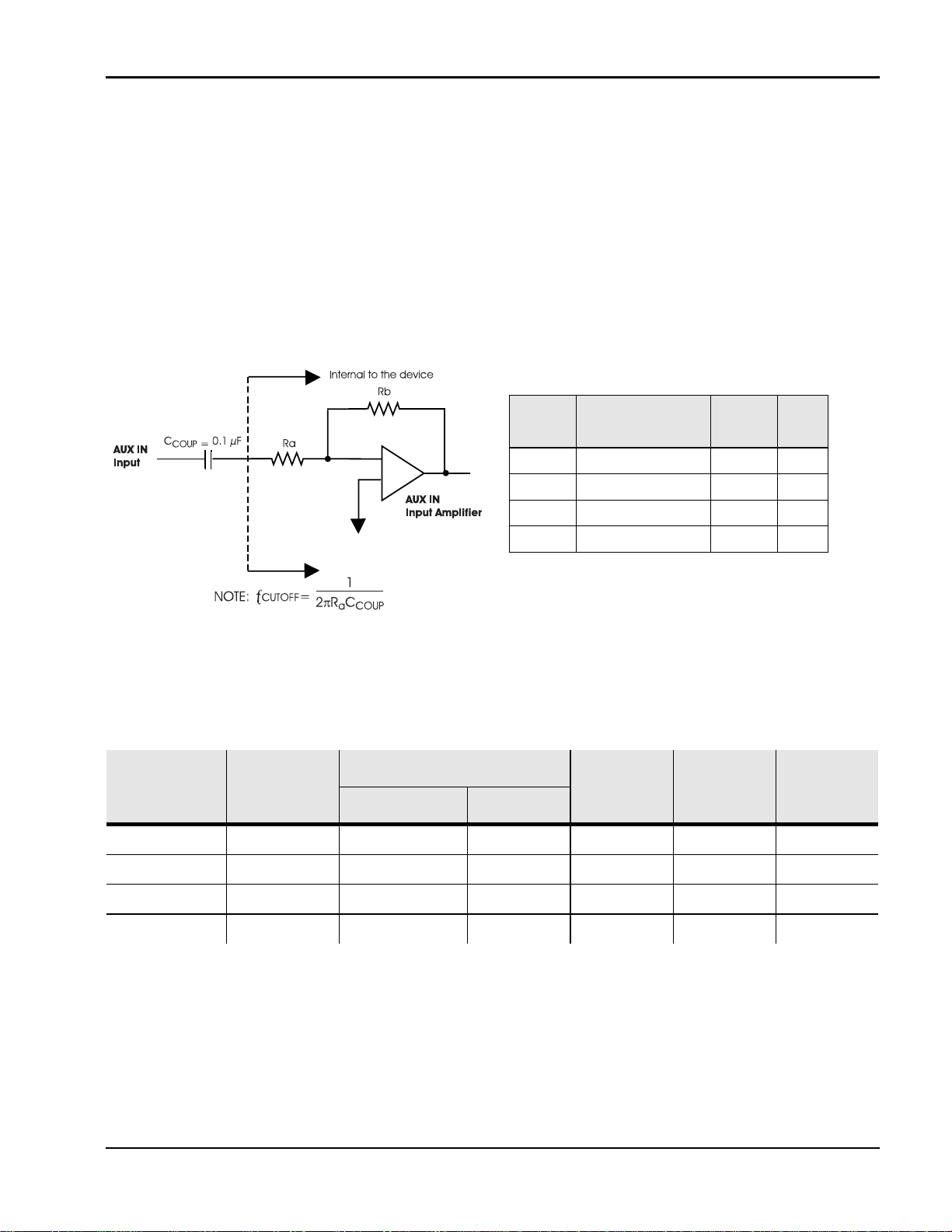
1.
2.
AUX IN (Auxiliary Input)
The AUX IN is an additional audio input to the
ISD5008, such as from the microphone circuit
in a mobile phone “car kit.” This input has a
nominal 700 mVp-p level at its minimum gain
setting (0 dB). See Table 5. Additional gain is
available in 3 dB steps (controlled by the SPI
bus) up to 9 dB.
Figure 3: AUX IN Input Modes
3.
4.
ISD5008 Product
Gain
Setting
Resistor Ratio
(Rb/Ra)
Gain
Gain
(dB)
00 40.1/40.1 1.0 0
01 47.0/33.2 1.414 3
10 53.5/26.7 2.0 6
11 59.2/21 2.82 9
Table 5: AUXIN Amplifier Gain Settings
Setting
(1)
0TLP Input
(3)
V
PP
AXG1
0 dB .694 0 0 1.00 .694 .694
CFG0
AXG0
Gain
(2)
Array In/Out
V
PP
Ana Out V
PP
(4)
3 dB .491 0 1 1.41 .694 .694
6 dB .347 1 0 2.00 .694 .694
9 dB .245 1 1 2.82 .694 .694
Gain from AUX IN to ANA OUT
Gain from AUX IN to ARRAY IN
0TLP Input is the reference Transmission Level Point that is used for testing. This level is typically 3 dB below clipping.
Differential
ISD
5
Page 10

ISD5008 Product
ANAOUT+/–(Analog Outputs)
This differential output is designed to go to the
microphone input of the telephone chip set. It
is designed to drive a minimum of 5 kΩ between the “+” and “–” pins to a nominal voltage level of 700 mVp-p. Both pins have DC
bias of approximately 1.2 VDC. The AC signal
is superimposed upon this analog ground voltage. These pins can be used single-ended,
getting only half the voltage. Do
NOT
ground
the unused pin.
AUX OUT (Auxiliary Output)
The AUXOUT is an additional audio output pin,
to be used, for example, to drive the speaker
circuit in a “car kit.” It drives a minimum load
of 5 kΩ and up to a maximum of 1 Vp-p. The
AC signal is superimposed on approximately
1.2 VDC bias and must be capacitively coupled to the load.
SP+, SP– (Speaker+/–)
This is the speaker differential output circuit. It
is designed to drive an 8 Ω speaker connected across the speaker pins up to a maximum
of 23.5 mW power. This stage has two selectable gains, 1.32 and 1.6, which can be chosen through the configuration registers. These
pins are biased to approximately 1.2 VDC
and, if used single-ended, must be capacitively coupled to their load. Do
the unused pin.
NOT
ground
2.3 POWER AND GROUND PINS
V
To minimize noise, the analog and digital circuits in the ISD5008 device uses separate
power busses. These +3 V busses lead to separate pins. Tie the V
as possible and decouple both supplies as
near to the package as possible.
V
The ISD5008 series utilizes separate analog
and digital ground busses. The analog ground
(V
the package as possible and connected
through a low-impedance path to power supply ground. The digital ground (V
should be connected through a separate
low-impedance path to power supply
ground. These ground paths should be large
enough to ensure that the impedance between the V
than 3 Ω . The backside of the die is connected to V
a chip-on-board design, the die attach area
must be connected to V
, V
CCA
, V
SSA
) pins should be tied together as close to
SSA
(Voltage Inputs)
CCD
pins together as close
CCD
(Ground Inputs)
SSD
pins and the V
SSA
through the substrate resistance. In
SSD
.
SSD
pin is less
SSD
SSD
) pin
ACAP (AGC Capacitor)
This pin provides the capacitor connection for
setting the parameters of the microphone
AGC circuit. It should have a 4.7 µF capacitor
connected to ground. It cannot be left
floating. This is because the capacitor is also
used in the playback mode for the AutoMute
circuit. This circuit reduces the amount of
noise present in the output during quiet
pauses. Tying this pin to ground gives
maximum gain; to V
gives minimum gain
CCA
for the AGC amplifier but will cancel the AutoMute function.
6
Voice Solutions in Silicon
™
Page 11
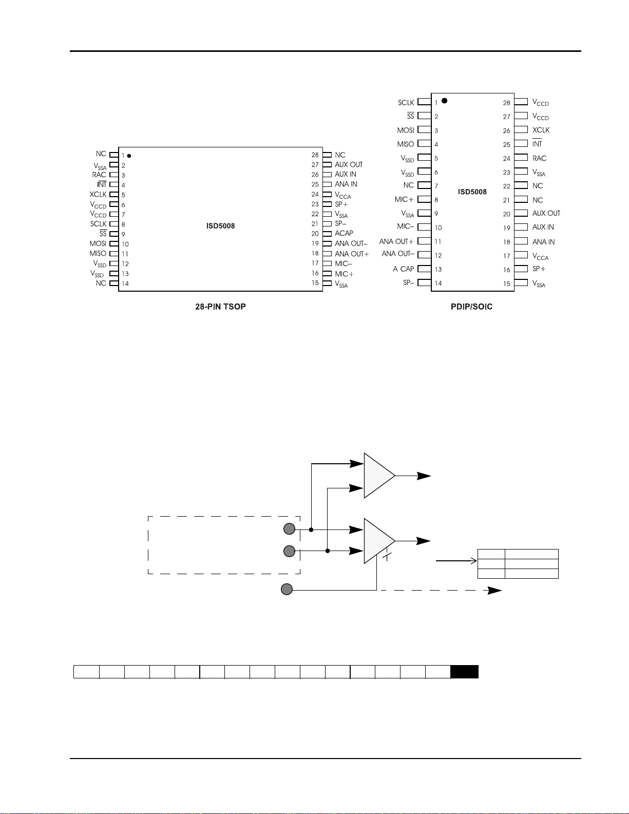
Figure 4: ISD5008 Series TSOP and PDIP/SOIC Pinouts
ISD5008 Product
3 INTERNAL FUNCTIONAL BLOCKS
Figure 5: Microphone Amplifier
*
6 dB
Microphone
(300 mVp-p Max)
1514131211109876543210
VLS1
VLS0 VOL2 VOL1 VOL0 S1S1 S1S0 S1M1 S1M0 S2M1 S2M0 FLS0 FLD1 FLD0 FLPD AGPD
MIC+
MIC–
ACAP
* Differential Path
AGC
1 (AGPD)
To AutoMute
(Playback Only)
FTHRU
AGC
AGPD
0 Power Up
1 Power Down
CFG1
ISD
7
Page 12
ISD5008 Product
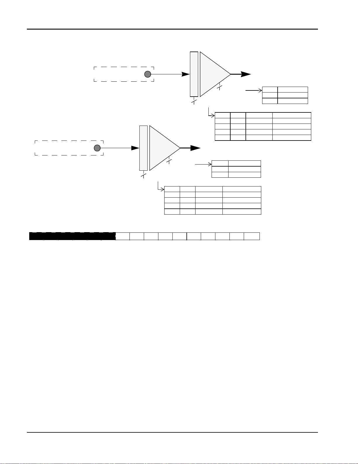
Figure 6: AUX IN and ANA IN
1.0 / 1.414 / 2.0 / 2.828
Car Kit AUX IN AUX IN AMP
AUX IN
AMP
1 (AXPD)
2 (AXG1, AXG0)
AXG1 AXG0 Input Gain 0TLP Input Level
.625 /.883 / 1.25 / 1.767
Chip Set ANA IN ANA IN AMP
ANA IN
AMP
1 (AIPD)
2 (AIG1,AIG0)
AIG1 AIG0 Input Gain 0TLP Input Level
0 0 0.625 1.11
0 1 0.883 .785
1 0 1.250 .555
1 1 1.767 .393
1514131211109876543210
AIG1
AIG0 AIPD AXG1 AXG0 AXPD INS0 AOS2 AOS1 AOS0 AOPD OPS1 OPS0 OPA1 OPA0 VLPD
0 0 1 .694
0 1 1.414 .491
1 0 2 .347
1 1 2.828 .245
AIPD
0 Power Up
1 Power Down
AXPD
0 Power Up
1 Power Down
CFG0
8
Voice Solutions in Silicon
™
Page 13
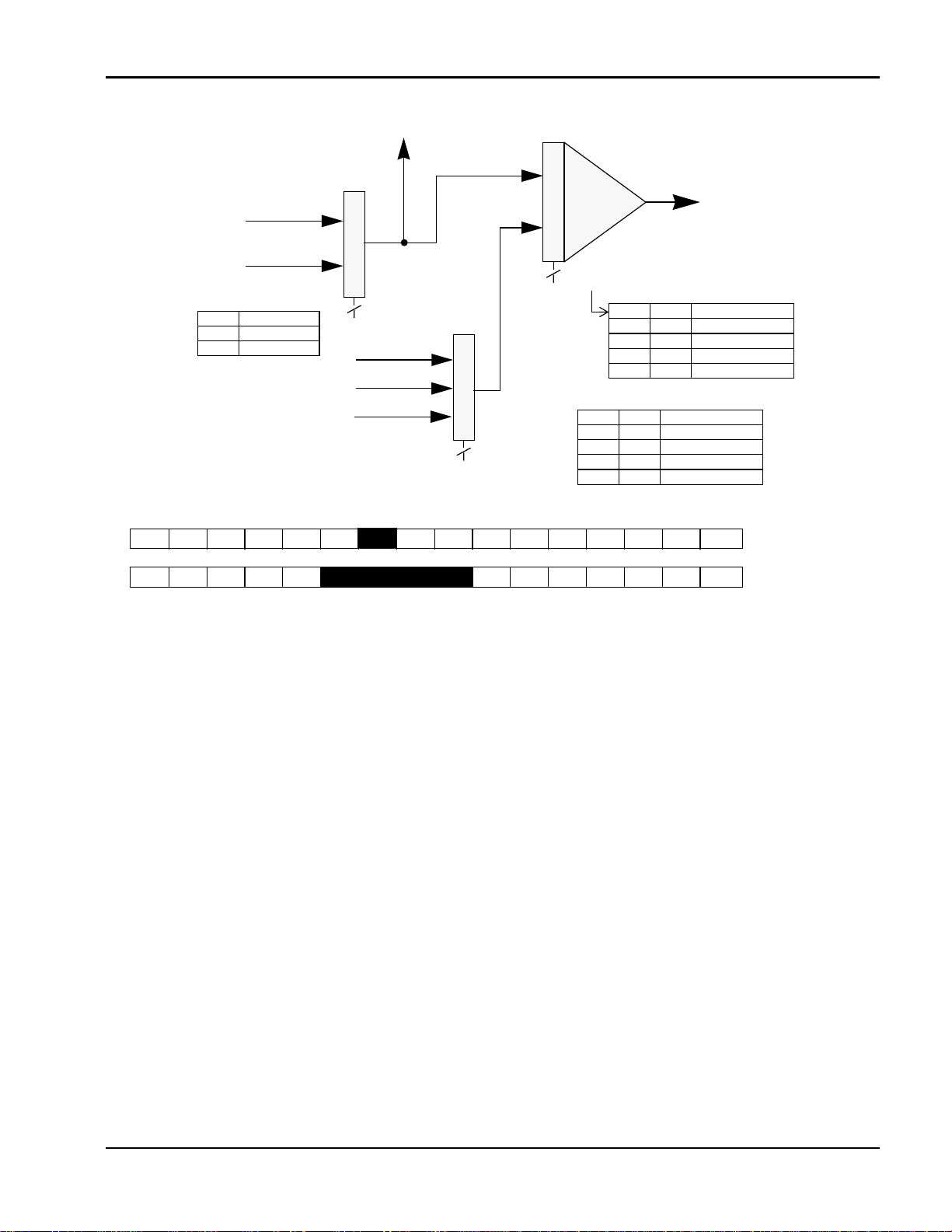
Figure 7: ISD5008 Core (Left Half)
ISD5008 Product
INPUT
SOURCE
SUM1 SUMMING
AMP
MUX
AGC AMP
Σ
SUM1
AUX IN AMP
2 (S1M1,S1M0)
INSO Source
0 AGC AMP
1 AUX IN AMP
(INS0)
FILTO
SUM1
MUX
ANA IN AMP
ARRAY
2 (S1S1,S1S0)
1514131211109876543210
AIG1
AIG0 AIPD AXG1 AXG0 AXPD INS0 AOS2 AOS1 AOS0 AOPD OPS1 OPS0 OPA1 OPA0 VLPD
1514131211109876543210
VLS1
VLS0 VOL2 VOL1 VOL0 S1S1 S1S0 S1M1 S1M0 S2M1 S2M0 FLS0 FLD1 FLD0 FLPD AGPD
S1M1 S1M0 SOURCE
00BOTH
0 1 SUM1 MUX ONLY
1 0 INP ONLY
1 1 Power Down
S1S1 S1S0 SOURCE
0 0 ANA IN
0 1 ARRAY
1 0 FILTO
1 1 N/C
CFG0
CFG1
ISD
9
Page 14
ISD5008 Product
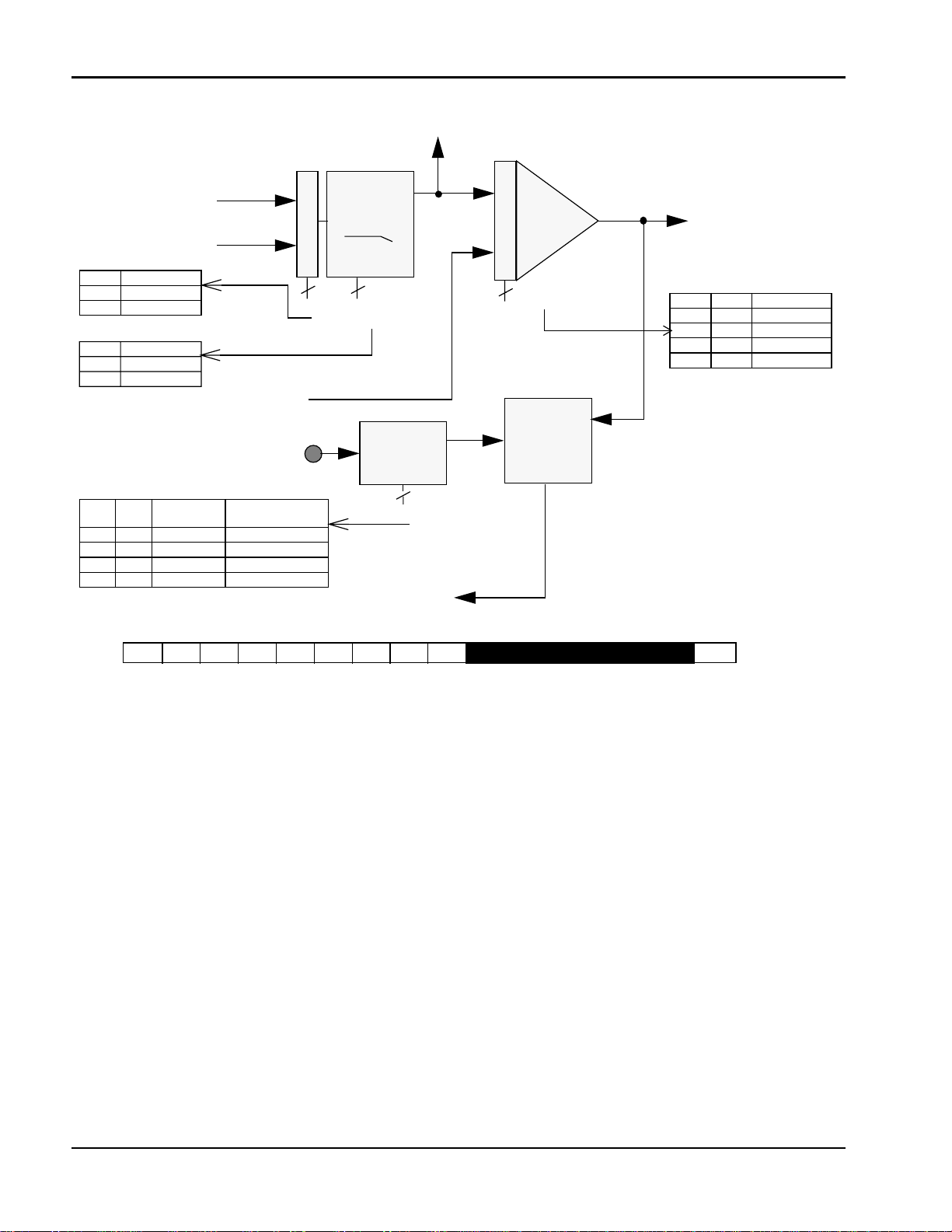
Figure 8: ISD5008 Core (Right Half)
SUM1
ARRAY
FLS0 Source
0 SUM1
1 ARRAY
FLPD
0 Power Up
1 Power Down
ANA IN AMP
FLD1 FLD0 SAMPLE
RATE
0 0 8 kHz 3.4 kHz
0 1 6.4 kHz 2.7 kHz
1 0 5.3 kHz 2.3 kHz
1 1 4 kHz 1.7 kHz
FILTER PASS BAND
FILTER
MUX
XCLK
FILTO
LOW PASS
FILTER
1
(FLS0)1 (FLPD)
INTERNAL
CLOCK
2
(FLD1,FLD0)
ARRAY
SUM2 SUMMING
AMP
Σ
2 (S2M1,S2M0)
MULTILEVEL
STORAGE
ARRAY
SUM2
S2M1 S2M0 SOURCE
00BOTH
0 1 ANA IN ONLY
1 0 FILTO ONLY
1 1 Power Down
1514131211109876543210
VLS1
VLS0 VOL2 VOL1 VOL0 S1S1 S1S0 S1M1 S1M0 S2M1 S2M0 FLS0 FLD1 FLD0 FLPD AGPD
CFG1
10
Voice Solutions in Silicon
™
Page 15
ANA IN AMP
SUM2
ISD5008 Product
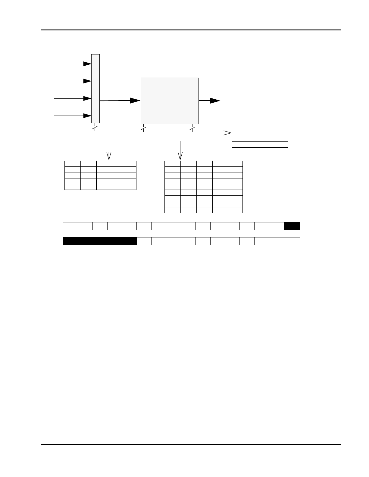
Figure 9: Volume Control
VOL
MUX
SUM1
VOLUME
CONTROL
VOL
INP
2
(VLS1,VLS0)
VLS1 VLS0 SOURCE
0 0 ANA IN AMP
0 1 SUM2
1 0 SUM1
1 1 INP
1514131211109876543210
AIG0 AIPD AXG1 AXG0 AXPD AOS2 AOS1 AOS0 AOPD OPS1 OPS0 OPA1 OPA0 VLPD
AIG1
1514131211109876543210
VLS1
VLS0 VOL2 VOL1 S1S1 S1S0 S1M1 S1M0 S2M1 S2M0 FLS0 FLD1 FLD0 FLPD AGPD
VOL0
3
(VOL2,VOL1,VOL0)
VOL2 VOL1 VOL0 Attenuation
0000 dB
0 0 1 –4 dB
0 1 0 –8 dB
0 1 1 –12 dB
1 0 0 –16 dB
1 0 1 –20 dB
1 1 0 –24 dB
1 1 1 –28 dB
INS0
1 (VLPD)
VLPD
0 Power Up
1 Power Down
CFG0
CFG1
ISD
11
Page 16
ISD5008 Product
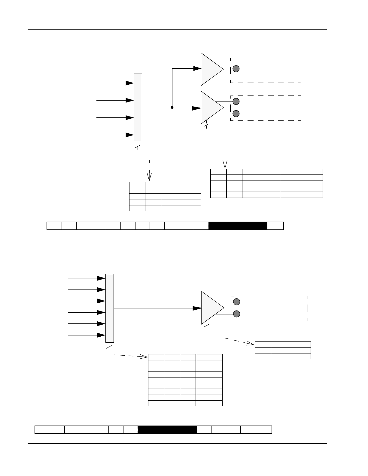
Figure 10: Speaker and AUX OUT
OUTPUT
MUX
AUX OUT
Car Kit
(1 Vp-p Max)
VOL
ANA IN AMP
FILTO
SUM2
SP+
SP–
2
(OPA1, OPA0)
Speaker
2
(OPS1,OPS0)
OPA1 OPA0 SPKR Drive AUX OP
0 0 Power Down Power Down
OPS1 OPS0 SOURCE
00VOL
0 1 ANA IN
1 0 FILTO
1 1 SUM2
1514131211109876543210
AIG1
AIG0 AIPD AXG1 AXG0 AXPD AOS2 AOS1 AOS0 AOPD OPS1 OPS0 OPA1 OPA0 VLPD
INS0
0 1 3.6 Vp-p @ 150 Ω Power Down
1 0 23 mWatt @ 8 Ω Power Down
1 1 Power Down 1 Vp-p Max @ 5kΩ
CFG0
Figure 11: ANA OUT Output
ANA OUT
*FTHRU
*INP
*VOL
*FILTO
*SUM1
*SUM2
*DIFFERENTIAL PATH
1514131211109876543210
AIG1
AIG0 AIPD AXG1 AXG0 AXPD AOS2 AOS1 AOS0 AOPD OPS1 OPS0 OPA1 OPA0 VLPD
MUX
3 (AOS2,AOS1,AOS0)
INS0
1
(AOPD)
AOS2 AOS1 AOS0
0 0 0 FTHRU
001INP
010VOL
011FILTO
1 0 0 SUM1
1 0 1 SUM2
110N/C
111N/C
(1 Vp-p max. from AUX IN or ARRAY)
(600 mVp-p max. from microphone input)
ANA OUT+
ANA OUT–
AOPD
0 Power Up
1 Power Down
Chip Set
CFG0
12
Voice Solutions in Silicon
™
Page 17

4 SERIAL PERIPHERAL INTERFACE (SPI) DESCRIPTION
ISD5008 Product
The ISD5008 product operates from an SPI serial interface. The SPI interface operates with the
following protocol.
The data transfer protocol assumes that the
microcontroller’s SPI shift registers are clocked
on the falling edge of the SCLK. With the
ISD5008, data is clocked in on the MOSI pin on
the rising clock edge. Data is clocked out on
the MISO pin on the falling clock edge.
1. All serial data transfers begin with the
falling edge of SS
2. SS
3. Data is clocked in on the rising clock
4. Play and Record operations are initiat-
5. The opcodes and address fields are as
is held LOW during all serial communications and held HIGH between instructions.
edge and data is clocked out on the
falling clock edge.
ed by enabling the device by asserting
the SS
and an address field to the ISD5008 device (refer to the Opcode Summary on
the page 14).
follows: <8 control bits> and <16 address bits>.
pin LOW, shifting in an opcode
pin.
The Interrupt will be cleared the next
time an SPI cycle is completed.
7. As Interrupt data is shifted out of the
ISD5008 MISO pin, control and address
data is simultaneously being shifted into
the MOSI pin. Care should be taken
such that the data shifted in is compatible with current system operation. It is
possible to read interrupt data and start
a new operation within the same SPI cycle.
8. An operation begins with the RUN bit set
and ends with the RUN bit reset.
9. All operations begin with the rising edge
of SS
.
4.1 MESSAGE CUEING
Message cueing allows the user to skip
through messages, without knowing the actual physical location of the message. This operation is used during playback. In this mode,
the messages are skipped 1600 times faster
than in normal playback mode. It will stop
when an EOM marker is reached. Then, the internal address counter will point to the next
message.
6. Each operation that ends in an EOM or
Overflow will generate an interrupt, including the Message Cueing cycles.
ISD
13
Page 18
ISD5008 Product
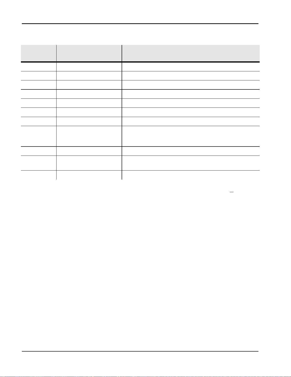
Table 6: Opcode Summary
Instruction
POWERUP 0010 0000 Power-Up: See “Power-Up Sequence”
LOADCFG0
LOADCFG1 00X0 0100 <D15–D0> Loads a 16-bit value into Configuration Register 1
SETPLAY 1110 0000 <A15–A0> Initiates Playback from address <A15–A0>
PLAY 1111 0000 Playback from current address (until EOM or OVF)
SETREC 1010 0000 <A15–A0> Initiates Record at address <A15–A0>
REC 1011 0000 Records from current address until OVF is reached
MC 1111 1000 Performs a Message Cue. Proceeds to the end of the current
STOP 0X11 0000 Stops current operation
STOPWRDN 0X01 0000 Stops current operation and enters stand-by (power-down)
RINT 0X11 0000 Read interrupt status bits: OVF and EOM.
(2)
Opcode <8 bits>
Address <16 bits>
00X0 0010 <D15–D0> Loads a 16-bit value into Configuration Register 0
(1)
Operational Summary
message (EOM) or enters OVF condition if it reaches the end
of the array.
mode.
1. X = Don’t Care.
2. Changes in CFG0 are not recognized until CFG1 is loaded. The changes will occur at the rising edge of SS
the cycle that CFG1 is loaded.
4.2 POWER-UP SEQUENCE
The ISD5008 will be ready for an operation after T
rate). The user needs to wait T
an operational command. For example, to
play from address 00 the following programing cycle should be used.
Playback Mode
(25 ms approximately for 8 kHz sample
PUD
before issuing
PUD
1. Send POWERUP command.
2. Wait T
(power-up delay).
PUD
3. Load CFG0 and CFG1 for desired operation.
4. Send SETPLAY command with address 00.
The device will start playback at address 00
and it will generate an interrupt when an EOM
is reached. It will then stop playback.
Record Mode
1. Send POWERUP command.
2. Wait T
3. Load CFG0 and CFG1 for desired operation.
4. Send POWERUP command.
5. Send SETREC command with
address 00.
The device will start recording at address 00
(power-up delay).
PUD
and it will generate an interrupt when an overflow is reached (end of memory array) or
when it has received a STOP command. It will
then stop recording.
during
14
Voice Solutions in Silicon
™
Page 19
ISD5008 Product
4.3 SPI PORT
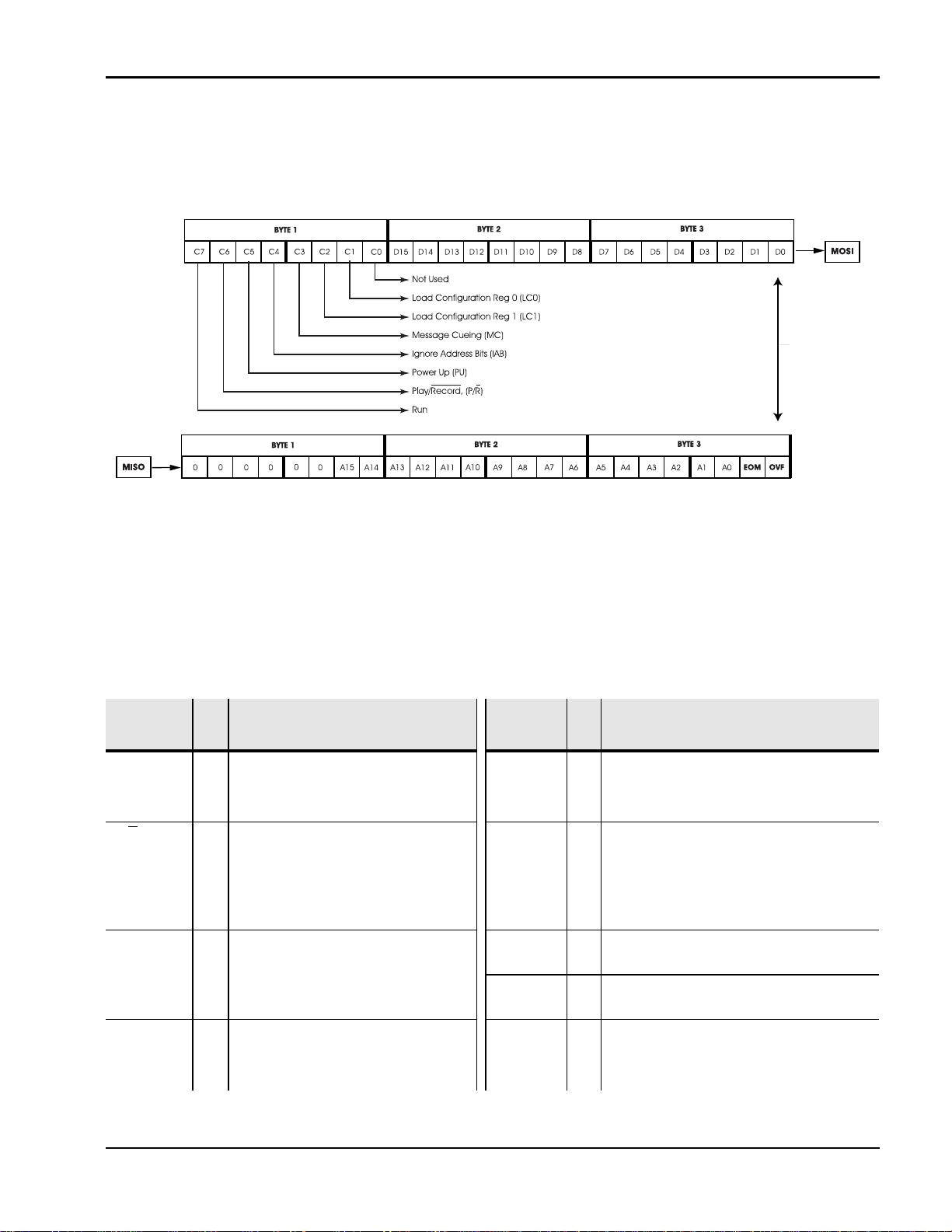
The following diagram describes the SPI port and the control bits associated with it.
Figure 12: SPI Port
LSB
NOTE: Bytes 2 and 3 of the MOSI input may be address bits or configuration bits, depending on the selected mode in byte 1.
4.4 SPI CONTROL REGISTER
The SPI control register provides control of individual device functions such as Play, Record, Message Cueing, Power-Up and Power-Down, Start and Stop operations, Ignore Address Pointers
and Load Configuration Registers.
Table 7: SPI Control Register
Control
Register
RUN Enable or Disable an operation PU Master power control
P/R Selects Play or Record
MC Enable or Disable Message
=
=
LC0 LC1
Bit Device Function
==10Start
Stop
operation
==10Play
Record
Cueing
10Enable Message Cueing
Disable Message Cueing
==10Load Configuration Reg 0
No Load
Control
Register
IAB Ignore address control bit
A15–A0 Output of the row pointer register
D15–D0 Input control and address register
Bit Device Function
==10Power-Up
Power-Down
==10Ignore input address register (A15–A0)
Use the input address register
contents for an operation (A15–A0)
==10Load Configuration Reg 1
No Load
ISD
15
Page 20
ISD5008 Product
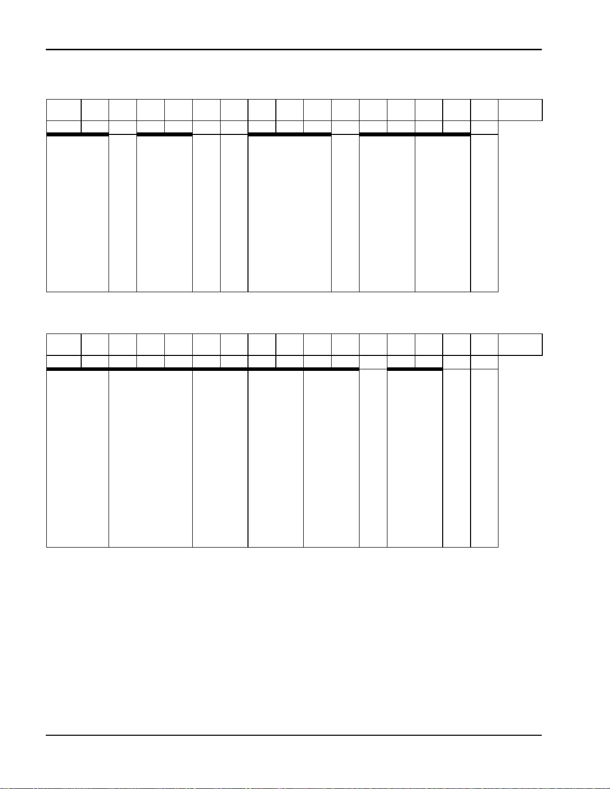
Table 8: Configuration Register 0
D15 D14 D13 D12 D11 D10 D9 D8 D7 D6 D5 D4 D3 D2 D1 D0
AIG1 AIG0 AIPD AXG1 AXG0 AXPD INS0 AOS2 AOS1 AOS0 AOPD OPS1 OPS0 OPA1 OPA0 VLPD
ANA IN AMP Gain SET (2 bits)
ANA IN Power Down
AUX IN AMP Gain SET (2 bits)
INPUT SOURCE MUX Select (1 bit)
ANA OUT MUX Select (3 bits)
AUX IN Power Down
ANA OUT Power Down
SPKR & AUX OUT Control (2 bits)
OUPUT MUX Select (2 bits)
Table 9: Configuration Register 1
D15 D14 D13 D12 D11 D10 D9 D8 D7 D6 D5 D4 D3 D2 D1 D0
VLS1 VLS0 VOL2 VOL1 VOL0 S1S1 S1S0 S1M1 S1M0 S2M1 S2M0 FLSO FLD1 FLD0 FLPD AGPD
VOLUME CONT. MUX Select (2 bits)
VOLUME CONTROL (3 bits)
SUM 1 MUX Select (2 bits)
SUM 1 SUMMING AMP Control (2 bits)
SUM2 SUMMING AMP Control (2 bits)
SAMPLE RATE (& Filter) Set Up (2 bits)
FILTER MUX Select
Filter Power Down
CFG0
Volume Control Power Down
CFG1
AGC AMP Power Down
16
Voice Solutions in Silicon™
Page 21
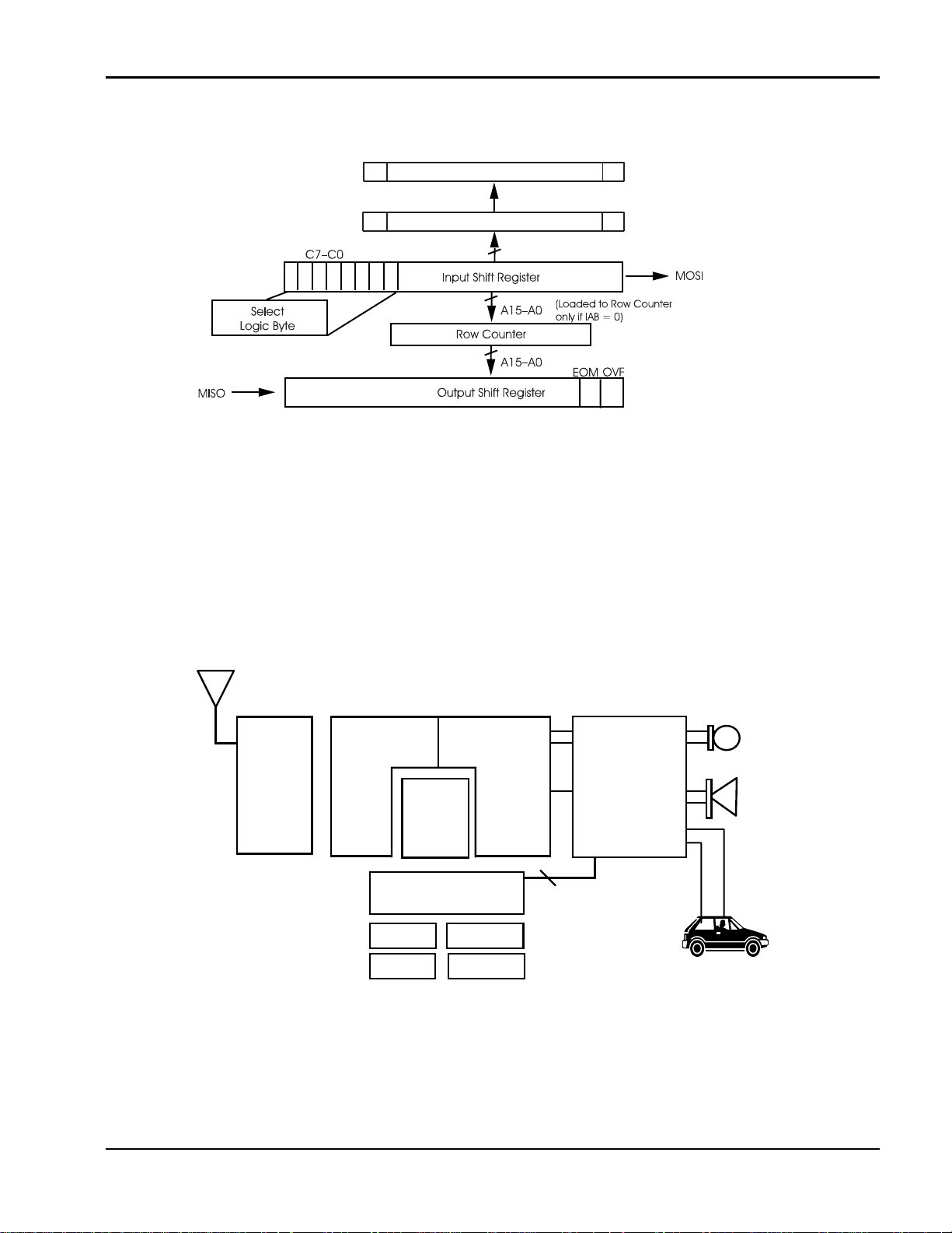
Figure 13: SPI Interface Simplified Block Diagram
Configuration Registers
D15
CFG1
(1)
D0
ISD5008 Product
1. See Table 8 for bit details.
D15
CFG0
D15 - D0
D0
Figure 14: Typical Digital Cellular Phone Integration
RF
Section
IF
Interface
DSP
Microcontroller
Keypad
Display
MIC IN+
MIC INÐ
SP OUT+
SP OUT
Voice Band
Codec
SPI
EEPROM
Flash
Ð
ISD5008
ANA OUT+
ANA OUT-
ANA IN
AUX OUT
SPI
Microphone
MIC+
MIC-
Earpiece
SP+
SPÐ
AUX IN
Car Kit
ISD
17
Page 22
ISD5008 Product
5 OPERATIONAL MODES DESCRIPTION
The ISD5008 can operate in many different
modes. It’s flexibility allows the user to configure the chip such that almost any input can
mixed with any other input and then be directed to any output. The variable settings for
the ANA and AUX input amplifiers plus the microphone AGC and speaker volume controls
make it possible to use the device with most
existing cell phone or cordless phone chip sets
with no external level adjustment. Several
modes will be found in most applications,
however. Please refer to the ISD5008 block diagram to better understand the following
modes. In all cases, we are assuming that the
chip has been powered up with the PU bit in
the SPI control register and that a time period
of T
has elapsed after that bit was set:
PUD
5.1 FEED THROUGH MODE
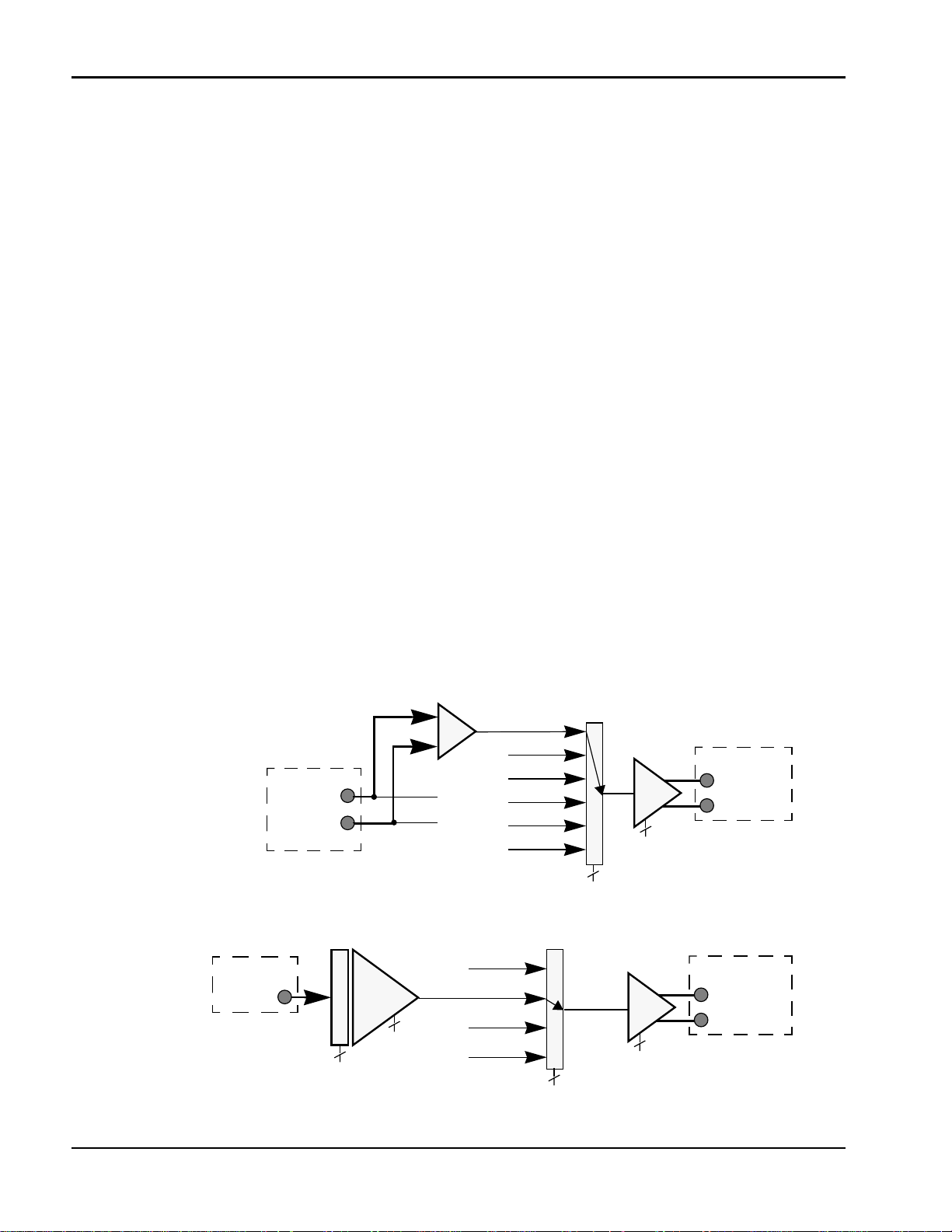
This mode enables the ISD5008 to connect to
a base band cell phone or cordless phone
chip set without affecting the audio source or
destination. There are two paths involved, the
transmit path and the receive path. The transmit path connects the ISD chip’s microphone
source through to the microphone input on
the base band chip set. The receive path
connects the base band chip set’s speaker
output through to the speaker driver on the
ISD chip. This allows the ISD chip to substitute
for those functions and incidentally gain access to the audio to and from the base band
chip set. Figure 14 shows one possible connection to such a chip set.
Figure 15 shows the part of the ISD5008 block
diagram that is used in Feed Through Mode.
The rest of the chip will be powered down to
conserve power. The bold lines highlight the
audio paths. Note that the Microphone to
ANA OUT +/– path is differential.
Chip Set
ANA IN
Figure 15: Basic Feed-Thru Mode
Microphone
MIC+
MIC–
.625 /.883 / 1.25 / 1.767
ANA IN
AMP
1 (AIPD)
2 (AIG1,AIG0)
6 dB
VOL
ANA IN AMP
FILTO
SUM2
FTHRU
INP
VOL
FILTO
SUM1
SUM2
ANA OUT
MUX
3 (AOS2,AOS1,AOS0)
OUTPUT
MUX
2
(OPS1,OPS0)
Chip Set
ANA OUT+
ANA OUT–
1
(AOPD)
Speaker
SP+
SP–
2
(OPA1, OPA0)
18
Voice Solutions in Silicon
™
Page 23

ISD5008 Product
To select this mode, the following control bits
must be configured in the ISD5008 configuration
registers. To set up the transmit path:
1.
Select the FTHRU path through the ANA OUT
MUX—
the state of the ANAOUT MUX. These are the
D6, D7 and D8 bits respectively of Configuration Register 0 (CFG0) and they should all
be ZERO to select the FTHRU path.
2.
Power up the ANA OUT amplifier
AOPD controls the power up state of ANA
OUT. This is bit D5 of CFG0 and it should be
a ZERO to power up the amplifier.
To set up the receive path:
1.
Set up the ANA IN amplifier for the correct
gain
settings of this amplifier. These are bits D14
and D15 respectively of CFG0. The input
level at this pin determines the setting of
this gain stage. Table 4 will help determine
this setting. In this example we will assume
that the peak signal never goes above 1
volt p-p single ended. That would enable
us to use the 9dB attenuation setting, or
where D14 is ONE and D15 is ZERO.
Bits AOS0, AOS1 and AOS2 control
—Bit
—Bits AIG0 and AIG1 control the gain
The status of the rest of the functions in the
ISD5008 chip must be defined before the configuration registers settings are updated:
1.
Power down the Volume Control Element
—Bit VLPD controls the power up
state of the Volume Control. This is bit D0 of
CFG0 and it should be set to a ONE to
power down this stage.
2.
Power down the AUX IN amplifier
AXPD controls the power up state of the
AUX IN input amplifier. This is bit D10 of
CFG0 and it should be set to a ONE to
power down this stage.
3.
Power down the SUM1 and SUM2 Mixer
amplifiers
SUM1 mixer and bits S2M0 and S2M1 control the SUM2 mixer. These are bits D7 and
D8 in CFG1 and bits D5 and D6 in CFG1 respectively. All 4 bits should be set to a ONE
to power down these two amplifiers.
4.
Power down the FILTER stage
controls the power up state of the FILTER
stage in the device. This is bit D1 in CFG1
and should be set to a ONE to power
down the stage.
—Bits S1M0 and S1M1 control the
—Bit
—Bit FLPD
2.
Power up the ANA IN amplifier
controls the power up state of ANA IN. This
is bit D13 of CFG0 and should be a ZERO to
power up the amplifier.
3.
Select the ANA IN path through the OUTPUT MUX
state of the OUTPUT MUX. These are bits D3
and D4 respectively of CFG0 and they
should be set to the state where D3 is ONE
and D4 is ZERO to select the ANA IN path.
4.
Power up the Speaker Amplifier
OPA0 and OPA1 control the state of the
Speaker and AUX amplifiers. These are bits
D1 and D2 respectively of CFG0. They
should be set to the state where D1 is ONE
and D2 is ZERO. This powers up the Speaker Amplifier and configures it for it’s higher
gain setting for use with a piezo speaker element and also powers down the AUX
output stage.
—Bits OPS0 and OPS1 control the
—Bit AIPD
—Bits
5.
Power down the AGC amplifier
AGPD controls the power up state of the
AGC amplifier. This is bit D0 in CFG1 and
should be set to a ONE to power down this
stage.
6.
Don’t Care bits
not used in Feed Through Mode. Their bits
may be set to either level. In this example
we will set all the following bits to a ZERO.
(a). Bit INS0, bit D9 of CFG0 controls the Input Source Mux. (b). Bits AXG0 and AXG1
are bits D11 and D12 respectively in CFG0.
They control the AUX IN amplifier gain setting. (c). Bits FLD0 and FLD1 are bits D2 and
D3 respectively in CFG1. They control the
sample rate and filter band pass setting.
(d). Bit FLS0 is bit D4 in CFG1. It controls the
FILTER MUX. (e). Bits S1S0 and S1S1 are bits
D9 and D10 of CFG1. They control the
SUM1 MUX. (f). Bits VOL0, VOL1 and VOL2
are bits D11, D12 and D13 of CFG1. They
—The following stages are
—Bit
ISD
19
Page 24

ISD5008 Product
control the setting of the Volume Control.
(g). Bits VLS0 and VLS1 are bits D14 and
D15 of CFG1. They control the Volume
Control MUX.
The end result of the above set up is
CFG0=0100 0100 0000 1011 (hex 440B)
and
CFG1=0000 0001 1110 0011 (hex 01E3).
Since both registers are being loaded, CFG0 is
loaded followed by the loading of CFG1. These
two registers must be loaded in this order. The internal set up for both registers will take effect
synchronously with the rising edge of SS
.
5.2 CALL RECORD
The call record mode adds the ability to record
the incoming phone call. In most applications,
the ISD5008 would first be set up for Feed
Through Mode as described above. When the
user wishes to record the incoming call, the set
up of the chip is modified to add that ability. For
the purpose of this explanation, we will use the
6.4 kHz sample rate during recording.
The block diagram of the ISD5008 shows that the
Multilevel Storage array is always driven from
the SUM2 SUMMING amplifier. The path traces
back from there through the LOW PASS Filter,
THE FILTER MUX, THE SUM1 SUMMING amplifier,
the SUM1 MUX, then from the ANA in amplifier.
Feed Through Mode has already powered up
the ANA IN amp so we only need to power up
and enable the path to the Multilevel Storage
array from that point:
1.
Select the ANA IN path through the SUM1
MUX
—Bits S1S0 and S1S1 control the state
of the SUM1 MUX. These are bits D9 and
D10 respectively of CFG1 and they
should be set to the state where both D9
and D10 are ZERO to select the ANA IN
path.
2.
Select the SUM1 MUX input (only) to the
S1 SUMMING amplifier
S1M1 control the state of the SUM1 SUM-
—Bits S1M0 and
MING amplifier. These are bits D7 and D8
respectively of CFG1 and they should be
set to the state where D7 is ONE and D8 is
ZERO to select the SUM1 MUX (only) path.
3.
Select the SUM1 SUMMING amplifier path
through the FILTER MUX
the state of the FILTER MUX. This is bit D4 of
CFG1 and it must be set to ZERO to select
the SUM1 SUMMING amplifier path.
4.
Power up the LOWPASS FILTER
controls the power up state of the LOWPASS FILTER stage. This is bit D1 of CFG1
and it must be set to ZERO to power up
the LOW PASS FILTER STAGE.
5.
Select the 6.4 kHz sample rate
and FLD1 select the Low Pass filter setting
and sample rate to be used during
record and playback. These are bits D2
and D3 of CFG1. To enable the 6.4 kHz
sample rate, D2 must be set to ONE and
D3 set to ZERO.
6.
Select the LOW PASS FILTER input (only) to
the S2 SUMMING amplifier
S2M1 control the state of the SUM2 SUMMING amplifier. These are bits D5 and D6
respectively of CFG1 and they should be
set to the state where D5 is ZERO and D6
is ONE to select the LOW PASS FILTER
(only) path.
In this mode, the elements of the original PASS
THROUGH mode do not change. The sections of
the chip not required to add the record path remain powered down. In fact, CFG0 does not
change and remains
CFG0=0100 0100 0000 1011 (hex 440B).
CFG1 changes to
CFG1=0000 0000 1100 0101 (hex 00C5).
Since CFG0 is not changed, it is only necessary
to load CFG1. Note that if only CFG0 was
changed, it would be necessary to load both
registers.
—Bit FLS0 controls
—Bit FLPD
—Bits FLD0
—Bits S2M0 and
20
Voice Solutions in Silicon
™
Page 25

ISD5008 Product
5.3 MEMO RECORD
The Memo Record mode sets the chip up to
record from the local microphone into the
chip’s Multilevel Storage Array. A connected
cellular telephone or cordless phone chip set
may remain powered down and is not active in
this mode. The path to be used is microphone
input to AGC amplifier, then through the INPUT
SOURCE MUX to the SUM1 SUMMING amplifier.
From there the path goes through the FILTER
MUX, the LOW PASS FILTER, the SUM2 SUMMING
amplifier, then to the MULTILEVEL STORAGE ARRAY. In this instance, we will select the 5.3 kHz
sample rate. The rest of the chip may be powered down.
1.
Power up the AGC amplifier
controls the power up state of the AGC
amplifier. This is bit D0 of CFG1 and must
be set to ZERO to power up this stage.
2.
Select the AGC amplifier through the INPUT SOURCE MUX
state of the INPUT SOURCE MUX. This is bit
D9 of CFG0 and must be set to a ZERO to
select the AGC amplifier.
3.
Select the INPUT SOURCE MUX (only) to
—Bit INS0 controls the
the S1 SUMMING amplifier
S1M1 control the state of the SUM1 SUMMING amplifier. These are bits D7 and D8
respectively of CFG1 and they should be
set to the state where D7 is ZERO and D8
is ONE to select the INPUT SOURCE MUX
(only) path.
4.
Select the SUM1 SUMMING amplifier path
through the FILTER MUX
the state of the FILTER MUX. This is bit D4 of
CFG1 and it must be set to ZERO to select
the SUM1 SUMMING amplifier path.
5.
Power up the LOWPASS FILTER—
controls the power up state of the LOWPASS FILTER stage. This is bit D1 of CFG1
and it must be set to ZERO to power up
the LOW PASS FILTER STAGE.
6.
Select the 5.3 kHz sample rate
and FLD1 select the Low Pass filter setting
and sample rate to be used during
—Bit FLS0 controls
—Bit AGPD
—Bits S1M0 and
Bit FLPD
—Bits FLD0
record and playback. These are bits D2
and D3 of CFG1. To enable the 5.3 kHz
sample rate, D2 must be set to ZERO and
D3 set to ONE.
7.
Select the LOW PASS FILTER input (only) to
the S2 SUMMING amplifier
S2M1 control the state of the SUM2 SUMMING amplifier. These are bits D5 and D6
respectively of CFG1 and they should be
set to the state where D5 is ZERO and D6
is ONE to select the LOW PASS FILTER
(only) path.
To set up the chip for Memo Record, the configuration registers are set up as follows:
CFG0=0010 0100 0010 0001 (hex 2421).
CFG1=0000 0001 0100 1000 (hex 0148).
Only those portions necessary for this mode are
powered up.
—Bits S2M0 and
5.4 MEMO AND CALL RECORD PLAYBACK
This mode sets the chip up for local playback of
messages recorded earlier. The playback path
is from the MULTILEVEL STORAGE ARRAY to the
FILTER MUX, then to the LOW PASS FILTER stage.
From there the audio path goes through the
SUM2 SUMMING amplifier to the VOLUME MUX,
through the VOLUME CONTROL then to the
SPEAKER output stage. We will assume that we
are driving a pizeo speaker element. This audio
was previously recorded at 8 kHz. All unnecessary stages will be powered down.
1.
Select the MULTILEVEL STORAGE ARRAY
path through the FILTER MUX
the state of the FILTER MUX. This is bit D4 of
CFG1 and must be set to ONE to select
the MULTILEVEL STORAGE ARRAY.
2.
Power up the LOWPASS FILTER
controls the power up state of the LOWPASS FILTER stage. This is bit D1 of CFG1
and it must be set to ZERO to power up
the LOW PASS FILTER STAGE.
3.
Select the 8.0 kHz sample rate
FLD0 and FLD1 select the Low Pass filter
—Bit FLS0,
—Bit FLPD
—Bits
ISD
21
Page 26

ISD5008 Product
setting and sample rate to be used during record and playback. These are bits
D2 and D3 of CFG1. To enable the 8.0 kHz
sample rate, D2 and D3 must be set to ZERO.
4.
Select the LOW PASS FILTER input (only) to
the S2 SUMMING amplifier
—Bits S2M0
and S2M1 control the state of the SUM2
SUMMING amplifier. These are bits D5 and
D6 respectively of CFG1 and they should
be set to the state where D5 is ZERO and
D6 is ONE to select the LOW PASS FILTER
(only) path.
5.
Select the SUM2 SUMMING amplifier path
through the VOLUME MUX
—Bits VLS0 and
VLS1 control the state VOLUME MUX.
These bits are bits D14 and D16, respectively of CFG1. They should be set to the
state where D14 is ONE and D15 is ZERO
to select the SUM2 SUMMING amplifier.
6.
Power up the VOLUME CONTROL LEVEL
Bit VLPD controls the power-up state of
the VOLUME CONTROL attenuator. This is
Bit D0 of CFG0. This bit must be set to a
ZERO to power-up the VOLUME CONTROL.
—
should be set to the state where D3 is
ZERO and D4 is a ZERO to select the VOLUME CONTROL.
9.
Power up the SPEAKER amplifier and select the HIGH GAIN mode
—Bits OPA0
and OPA1 control the state of the speaker (SP+ and SP–) and AUX OUT outputs.
These are bits D1 and D2 of CFG0. They
must be set to the state where D1 is ONE
and D2 is ZERO to power-up the speaker
outputs in the HIGH GAIN mode and to
power-down the AUX OUT.
To set up the chip for Memo or Call Record/
Playback, the configuration registers are set up
as follows:
CFG0=0010 0100 0010 0001 (hex 2421).
CFG1=0000 0001 0100 1000 (hex 59D1).
Only those portions necessary for this mode are
powered up.
7.
Select a VOLUME CONTROL LEVEL
VOL0, VOL1, and VOL2 control the state
of the VOLUME CONTROL LEVEL. These
are bits D11, D12, and D13, respectively,
of CFG1. A binary count of 000 through
111 controls the amount of attenuation
through that state. In most cases, the software will select an attenuation level according to the desires of the current users
of the product. In this example, we will assume the user wants an attenuation of –
12 dB. For that setting, D11 should be set
to ONE, D12 should be set to ONE, and
D13 should be set to a ZERO.
8.
Select the VOLUME CONTROL path
through the OUTPUT MUX—
These are bits
D3 and D4, respectively, of CFG0. They
—Bits
22
Voice Solutions in Silicon
™
Page 27
ISD5008 Product
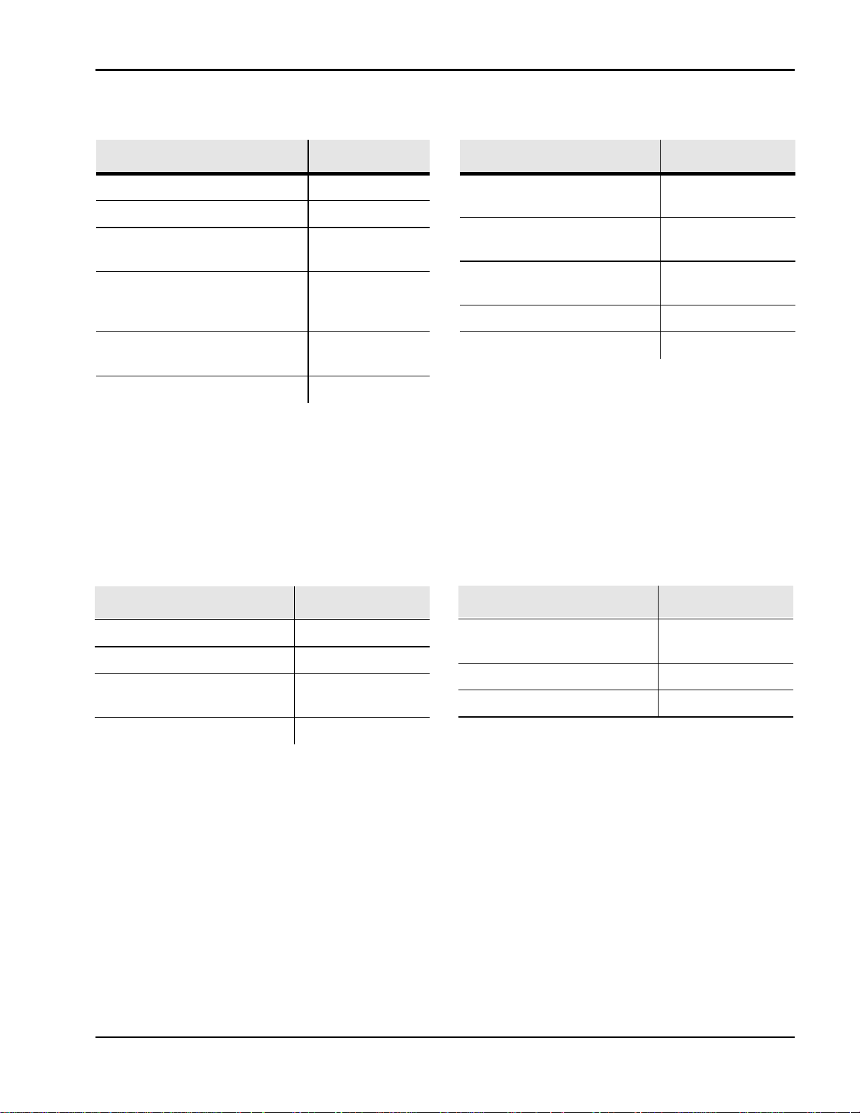
Table 10: Absolute Maximum Ratings
(Packaged Parts)
Condition Value
Junction temperature 150°C
Storage temperature range –65°C to +150°C
Voltage applied to any pin (VSS – 0.3 V) to
Voltage applied to any pin
(Input current limited to
±20 mA)
Lead temperature
(soldering – 10 seconds)
VCC – V
1. Stresses above those listed may cause permanent
SS
damage to the device. Exposure to the absolute
maximum ratings may affect device reliability.
Functional operation is not implied at these
conditions.
(1)
(VCC + 0.3 V)
(VSS – 1.0 V) to
(VCC + 1.0 V)
300°C
–0.3 V to +7.0 V
Table 12: Operating Conditions
(Packaged Parts)
Condition Value
Commercial operating
temperature range
(1)
Extended operating
temperature
(1)
Industrial operating
temperature
(1)
Supply voltage (VCC)
Ground voltage (VSS)
1. Case temperature
2. V
3. VSS = V
CC
= V
CCA
SSA
= V
= V
SSD
CCD
(2)
(3)
0°C to +70°C
–20°C to +70°C
–40°C to +85°C
+2.7 V to +3.3 V
0 V
Table 11: Absolute Maximum Ratings
(1)
(Die)
Condition Value
Junction temperature 150˚C
Storage temperature range –65˚C to +150˚C
Voltage applied to any pad (VSS – 0.3 V) to (VCC
+ 0.3 V)
VCC – V
1. Stresses above those listed may cause permanent
SS
damage to the device. Exposure to the absolute
maximum ratings may affect device reliability.
Functional operation is not implied at these
conditions.
–0.3 to +7.0 V
Table 13: Operating Conditions
(Die)
Condition Value
Commercial operating
temperature range
Supply voltage (VCC)
Ground voltage (VSS)
1. VCC = V
2. VSS = V
CCA
SSA
= V
= V
SSD
CCD
(1)
(2)
0˚C to +50˚C
+2.7 V to +3.3 V
0 V
ISD
23
Page 28
ISD5008 Product
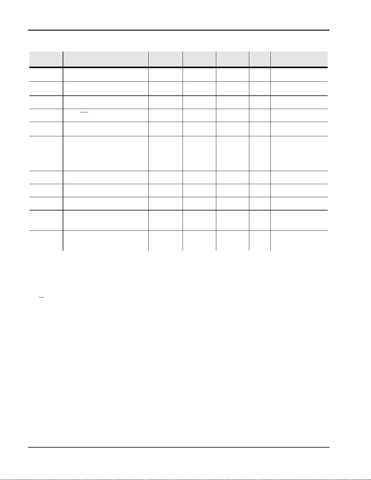
Table 14: DC Parameters
Symbol Parameters Min
V
V
V
V
V
I
IL
IH
OL
OL1
OH
CC
Input Low Voltage V
Input High Voltage V
Output Low Voltage 0.4 V IOL = 10 µA
RAC, INT Output Low Voltage 0.4 V IOL = 1 mA
Output High Voltage V
VCC Current (Operating)
— Playback
— Record
— Feedthru
I
SB
I
IL
I
HZ
R
ANA IN
VCC Current (Standby) 1 10 µA (3) (4)
Input Leakage Current ±1 µA
MISO Tristate Current 1 10 µA
ANA IN Input Resistance 60 to 102 kΩ See Ra in table in
(2)
x 0.8 V
CC
– 0.4 V IOH = –10 µA
CC
15
25
12
Typ
(1)
Max
x 0.2 V
CC
(2)
Units Conditions
mA
mA
mA
No load
No load
No load
Figure 2
(3)
(3)
(3)
R
AUX IN
AUX IN Input Resistance 21 to 40 kΩ See Ra in table in
Figure 3
1. Typical values: TA = 25°C and Vcc = 3.0 V.
2. All min/max limits are guaranteed by ISD via electrical testing or characterization. Not all specifications are
100 percent tested.
3. V
CCA
4. SS = V
and V
CCA
summed together.
CCD
= V
XCLK = MOSI = V
CCD,
SSA
= V
and all other pins floating.
SSD
24
Voice Solutions in Silicon™
Page 29

Symbol Characteristic Min
F
S
F
CF
T
REC
T
PLAY
T
PUD
T
STOP
T
RAC
T
RACLO
OR
PAUSE
Sampling Frequency 8.0
Filter Pass Band
8.0 kHz (sample rate)
6.4 kHz (sample rate)
5.3 kHz (sample rate)
4.0 kHz (sample rate)
Record Duration
8.0 kHz (sample rate)
6.4 kHz (sample rate)
5.3 kHz (sample rate)
4.0 kHz (sample rate)
Playback Duration
8.0 kHz (sample rate)
6.4 kHz (sample rate)
5.3 kHz (sample rate)
4.0 kHz (sample rate)
Power-Up Delay
8.0 kHz (sample rate)
6.4 kHz (sample rate)
5.3 kHz (sample rate)
4.0 kHz (sample rate)
Stop or Pause
Record or Play
8.0 kHz (sample rate)
6.4 kHz (sample rate)
5.3 kHz (sample rate)
4.0 kHz (sample rate)
RAC Clock Period
8.0 kHz (sample rate)
6.4 kHz (sample rate)
5.3 kHz (sample rate)
4.0 kHz (sample rate)
RAC Clock Low Time
8.0 kHz (sample rate)
6.4 kHz (sample rate)
5.3 kHz (sample rate)
4.0 kHz (sample rate)
Table 15: AC Parameters
(2)
Typ
31.25
37.5
62.5
31.25
37.5
(1)
6.4
5.3
4.0
3.4
2.7
2.3
1.7
25
50
50
75
100
200
250
300
400
25
50
Max
4
5
6
8
4
5
6
8
(2)
Units Conditions
(5)
kHz
(5)
kHz
(5)
kHz
(5)
kHz
3-dB Roll-Off Point
kHz
3-dB Roll-Off Point
kHz
3-dB Roll-Off Point
kHz
3-dB Roll-Off Point
kHz
(6)
min
(6)
min
(6)
min
(6)
min
(6)
min
(6)
min
(6)
min
(6)
min
msec
msec
msec
msec
msec
msec
msec
msec
msec
msec
msec
msec
(9)
(9)
(9)
(9)
msec
msec
msec
msec
ISD5008 Product
(3) (7)
(3) (7)
(3) (7)
(3) (7)
ISD
25
Page 30
ISD5008 Product
Symbol Characteristic Min
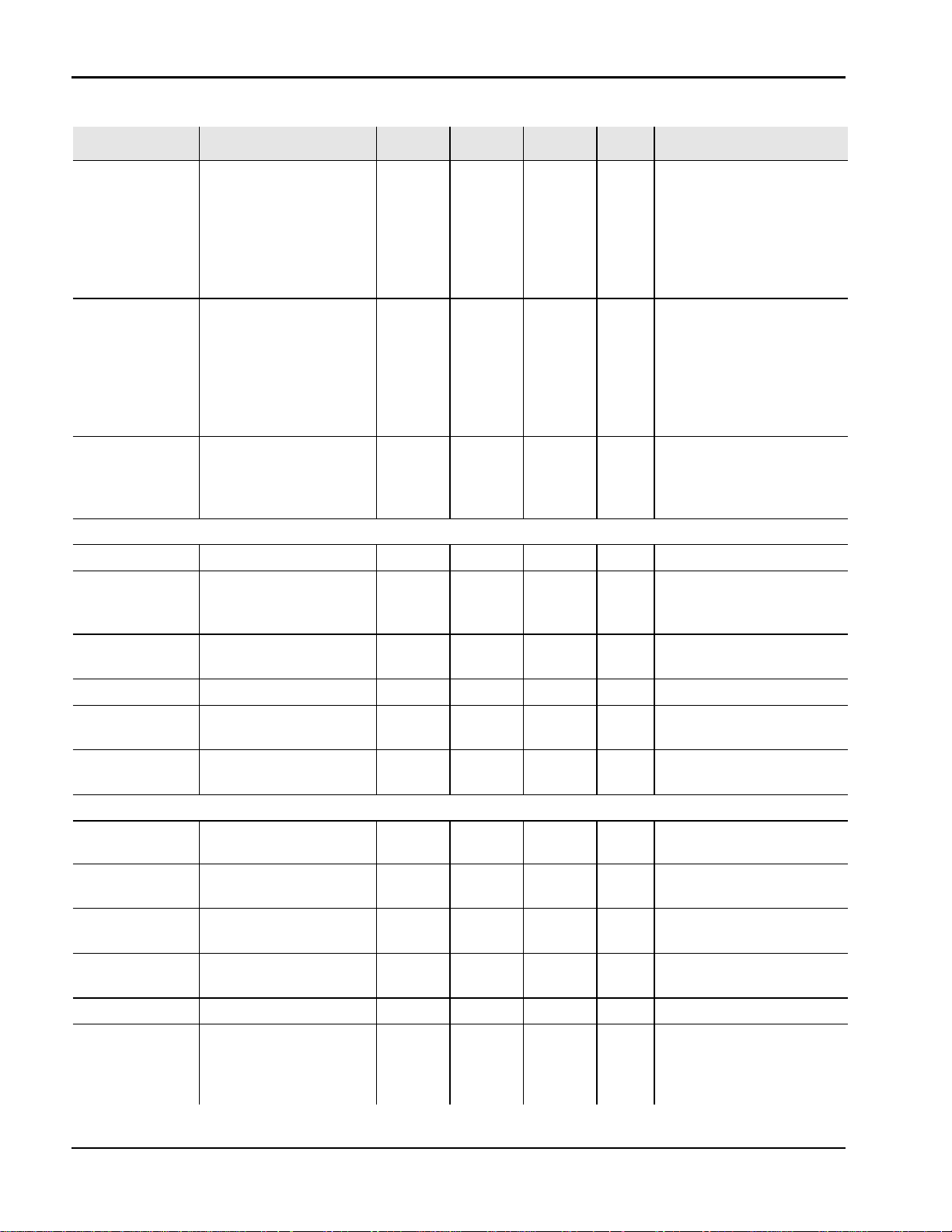
Table 15: AC Parameters
(2)
Typ
(1)
Max
(2)
Units Conditions
T
RACM
RAC Clock Period in
Message Cueing
Mode
8.0 kHz (sample rate)
6.4 kHz (sample rate)
5.3 kHz (sample rate)
4.0 kHz (sample rate)
T
RACML
RAC Clock Low Time in
Message Cueing
Mode
8.0 kHz (sample rate)
6.4 kHz (sample rate)
5.3 kHz (sample rate)
4.0 kHz (sample rate)
THD Total Harmonic
Distortion
ANA IN to ARRAY,
ARRAY to SPKR
MICROPHONE INPUT
V
MIC+/–
V
MIC (0TLP)
MIC +/– Input Voltage 3 300 mV
MIC +/– input
reference transmission
level point (0TLP)
A
MIC
Gain from MIC+/–
input to ANA OUT
A
MIC (GT)
R
Microphone input
MIC
MIC +/– Gain Tracking ±0.1 dB
resistance
A
AGC
Microphone AGC
Amplifier Range
ANA IN
V
ANA IN
V
ANA IN (0TLP)
ANA IN Input Voltage 1.6 V
ANA IN (0TLP) Input
Voltage
A
ANA IN (SP)
Gain from ANA IN to
SP+/–
A
ANA IN (AUX OUT)
Gain from ANA IN to
AUX OUT
A
ANA IN (GA)
A
ANA IN (GT)
ANA IN Gain Accuracy –0.5 +0.5 dB
ANA IN Gain Tracking ±0.1 dB
125
156.3
187.5
250
15.63
19.53
23.44
31.25
12%
208 mV
5.5 6.0 6.5 dB
51015
640dB
1.11 V
6 to 15 dB
–4 to +5 dB
µsec
µsec
µsec
µsec
µsec
µsec
µsec
µsec
k
Ω
@1 kHz at 0TLP, sample rate =
5.3kHz
Peak-to-Peak
Peak-to-Peak
1 kHz at V
1 kHz, +3 to –40 dB 0TLP Input
MIC– and MIC+ pins
Over 3–300 mV Input Range
Peak-to-Peak (6dB gain
setting)
Peak-to-Peak (6dB gain
setting)
4 Steps of 3 dB
4 Steps of 3 dB
(11)
1000 Hz, +3 to
–40 dB 0TLP Input, 6dB setting
MIC (0TLP)
(10)
(4)(8)
(4)(10)
(4)
26
Voice Solutions in Silicon™
Page 31
Symbol Characteristic Min
AUX IN
V
AUX IN
V
AUX IN (0TLP)
AUX IN Input Voltage 1.0 V
AUX IN (0TLP) Input
Voltage
A
AUX IN (ANA OUT)
Gain from AUX IN to
ANA OUT
A
AUX IN (GA)
A
Aux IN (GT)
AUX IN Gain Accuracy –0.5 +0.5 dB
AUX IN Gain Tracking ±0.1 dB
SPEAKER OUTPUTS
V
SPHG
SP+/– Output Voltage
(High Gain setting)
R
SPLG
SP+/– Output Load
Imp. (Low Gain)
R
SPHG
SP+/– Output Load
Imp. (High Gain)
C
SP
SP+/– Output Load
Cap.
V
SPAG
SP+/– Output Bias
Voltage (analog
ground)
V
SPDCO
Speaker Output DC
Offset
ICN
ANA IN/SP+/–
ANA IN to SP+/– Idle
Channel Noise
CRT
SP+/–
SP+/– to ANA OUT
Cross talk
PSRR Power Supply
Rejection Ratio
F
R
Frequency Response
(300–3400 Hz)
P
OUTLG
Power Output (Low
Gain Setting)
SINAD SINAD ANA IN to
SP+/–
ANA OUT
V
(ANA OUT 0TLP)
ANA OUT 0TLP 694 mV
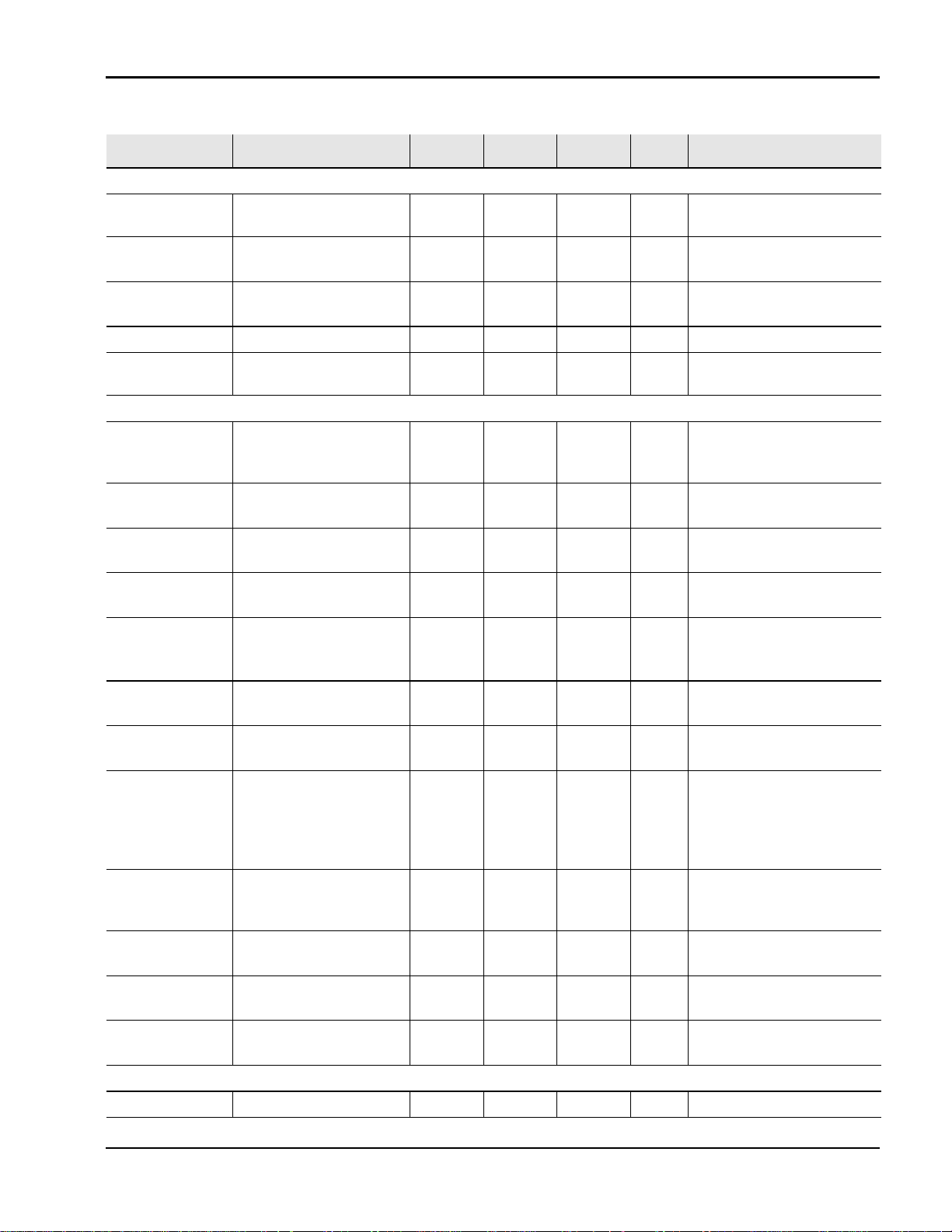
Table 15: AC Parameters
(2)
8 Ω
70 Ω
–100 100 mVD
–65 dB
–65 dB
–0.25 +0.25 dB
62.5 dB
(1)
Typ
Max
694.2 mV
0 to 9 dB
1.2 VDC
–50 dB
(2)
Units Conditions
3.6 V
100 pF
23.5 mW
RMS
ISD5008 Product
Peak-to-Peak (0 dB gain
setting)
Peak-to-Peak (0 dB gain
setting)
4 Steps of 3dB
(11)
1000 Hz, +3 to
–40 dB 0TLP Input, 0dB setting
Peak-to-Peak, differential
load = 150Ω; OPA1, OPA0 =
01
OPA1, OPA0 = 10
OPA1, OPA0 = 01
With ANA IN to Speaker, ANA
IN AC coupled to V
C
Speaker load = 150Ω
With 0TLP input to ANA IN,
with MIC+/– and AUX IN AC
coupled to V
measured at ANA OUT @
1 kHz, feedthrough mode
Measured with a 1kHz,100
mVpp sine wave input at
V
With 0TLP input to ANA IN,
6dB setting
Differential load at 8Ω
0TLP ANA IN input minimum
gain, 5k Ω load
peak-to-peak
CCA
(10)
and V
SSA
CCD
(12)
, and
pins
(12)
SSA
(12)13)
(12)
ISD
27
Page 32
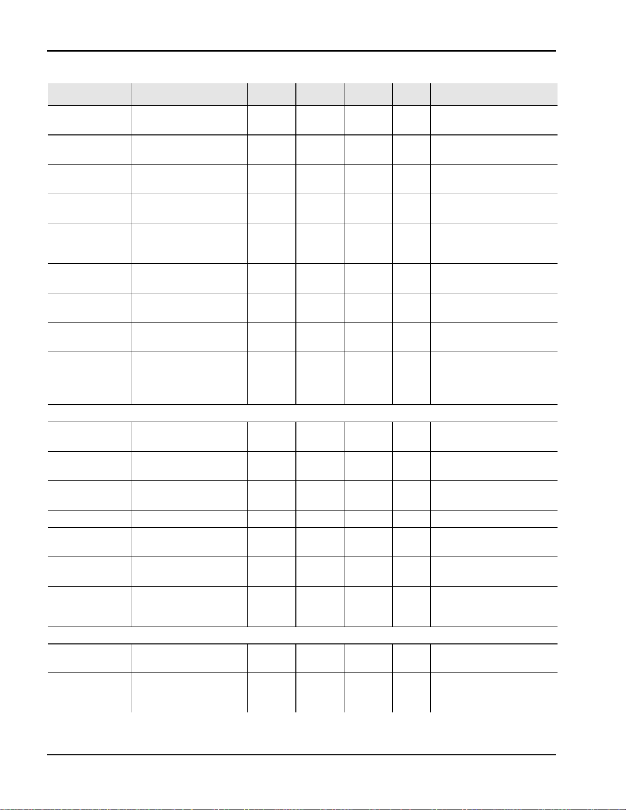
ISD5008 Product
Symbol Characteristic Min
SINAD SINAD MIC IN to ANA
OUT
SINAD SINAD AUX IN to ANA
OUT (0 to 9 dB)
ICN
MIC/ANAOUT
ICN
AUX IN/
ANAOUT
PSRR
(ANA OUT)
V
BIAS
V
OFFSET
R
L
F
R
AUX OUT
V
AUX OUT
R
L
C
L
V
BIAS
SINAD SINAD—ANA IN to AUX
ICN
(AUX OUT)
CRT
AUXOUT
VOLUME CONTROL
A
OUT
Idle Channel Noise—
Microphone
Idle Channel Noise—
AUX IN (0 to 9 dB)
Power Supply
Rejection Ratio
ANA OUT+ and ANA
OUT–
ANA OUT+ to ANA
OUT–
Minimum Load
Impedence
Frequency Response
(300–3400 Hz)
AUX OUT—Maximum
Output Swing
Minimum Load
Impedence
Maximum Load
Capacitance
AUX OUT 1.2 VDC
OUT
Idle Channel Noise—
ANA IN to AUX OUT
Crosstalk—ANA IN/AUX
OUT path to ANA OUT
Output Gain –28 to 0 dB
Gain Accuracy -0.5 0.5 dB
Table 15: AC Parameters
(2)
62.5 dB
62.5 dB
–100 +100 mVD
5kΩ
–0.25 +0.25 dB
5kΩ
62.5 dB
(1)
Typ
Max
-50 dB
1.2 VDC
(2)
Units Conditions
–65 dB
–65 dB
1.0 Vpp
100 pF
–65 dB
–65 dB
, V
CCD
(12)13)
(12)13)
(12)13)
(12)13)
pins
Load = 5k Ω
Load = 5k Ω
Load = 5k Ω
Load = 5k Ω
Measured with a 1kHz,
100mVpp sine wave to
V
CCA
Inputs AC coupled to V
Inputs AC coupled to V
C
Differential Load
0TLP input to MIC+/- in
feedthrough mode, with
0TLP input to AUX IN in
feedthrough mode
5 kΩ Load
Measured 300–3400 Hz, @
1 kHz, Load = 5kΩ
Measured 300–3400 Hz, Load
= 5kΩ
AUX OUT 1 kHz @ 0TLP, AUX IN
and MIC+/– AC ANA OUT
load = 5kΩ coupled to V
8 Steps of 4 dB, referenced
to output
ANA IN = 1 kHz 0TLP, 6dB Gain
setting measured
differentially at SP+/–
SSA
SSA
(12)
SSA
28
Voice Solutions in Silicon™
Page 33

ISD5008 Product
1. Typical values: TA = 25˚C and Vcc = 3.0V.
2. All min/max limits are guaranteed by ISD via electrical testing or characterization. Not all specifications are
100 percent tested.
3. Low-frequency cut off depends upon the value of external capacitors (see Pin Descriptions).
4. Differential input mode. Nominal differential input is 208 mVp-p. (0 dBm0)
5. Sampling frequency can vary as much as –6/+4 percent over the industrial temperature and voltage ranges. For
greater stability, an external clock can be utilized (see Pin Descriptions). Sampling frequency will be accurate within
±1% for 5.3kHz, and ±5% for 4.0, 6.4 and 8.0 kHz sampling rates at room temperature.
6. Playback and Record Duration can vary as much as –4/+6 percent over the industrial temperature and voltage
ranges. For greater stability, an external clock can be utilized (See Pin Descriptions). Playback and record durations
are accurate within ±1% for 5.3kHz, and ±5% for 4.0, 6.4 and 8.0kHz sampling rates at room temperature.
7. Filter specification applies to the low pass filter. Therefore, from input to output, expect a 6 dB drop by nature of
passing through the filter twice.
8. For optimal signal quality, this maximum limit is recommended.
9. When a record command is sent, T
10. The maximum signal level at any input is defined as 3.17dB higher than the reference transmission level point. (0TLP)
This is the point where signal clipping may begin.
11. Measured at 0TLP point for each gain setting. See Table 4 and Table 5.
12. 0TLP is the reference test level through inputs and outputs. See Table 4 and Table 5.
13. Referenced to 0TLP input at 1kHz, measured over 300 to 3,400 Hz bandwidth.
RAC
= T
RAC
+ T
on the first row addressed.
RACLO
ISD
29
Page 34
ISD5008 Product
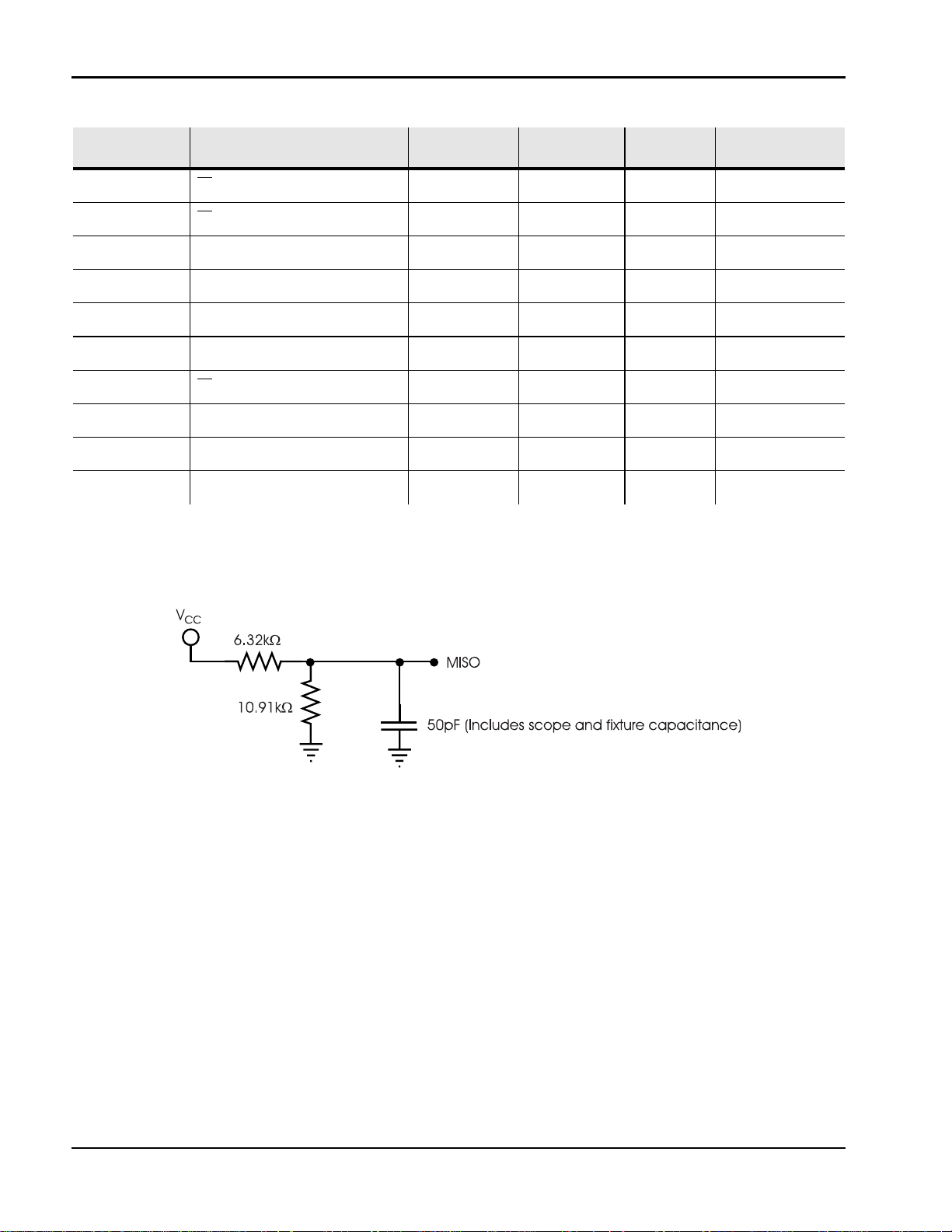
Table 16: SPI AC Parameters
(1)
Symbol Characteristics Min Max Units Conditions
T
SSS
T
SSH
T
DIS
T
DIH
T
PD
T
DF
T
SSmin
T
SCKhi
T
SCKlow
F
0
1. Typical values: TA= 25°C and Vcc= 3.0 V. Timing measured at 50 percent of the VCC level.
2. Tristate test condition
SS Setup Time 500 nsec
SS Hold Time 500 nsec
Data in Setup Time 200 nsec
Data in Hold Time 200 nsec
Output Delay 500 nsec
Output Delay to hiZ 500 nsec
SS HIGH 1 µsec
SCLK High Time 400 nsec
SCLK Low Time 400 nsec
CLK Frequency 1,000 kHz
(2)
30
Voice Solutions in Silicon™
Page 35
6 TIMING DIAGRAMS
ISD5008 Product
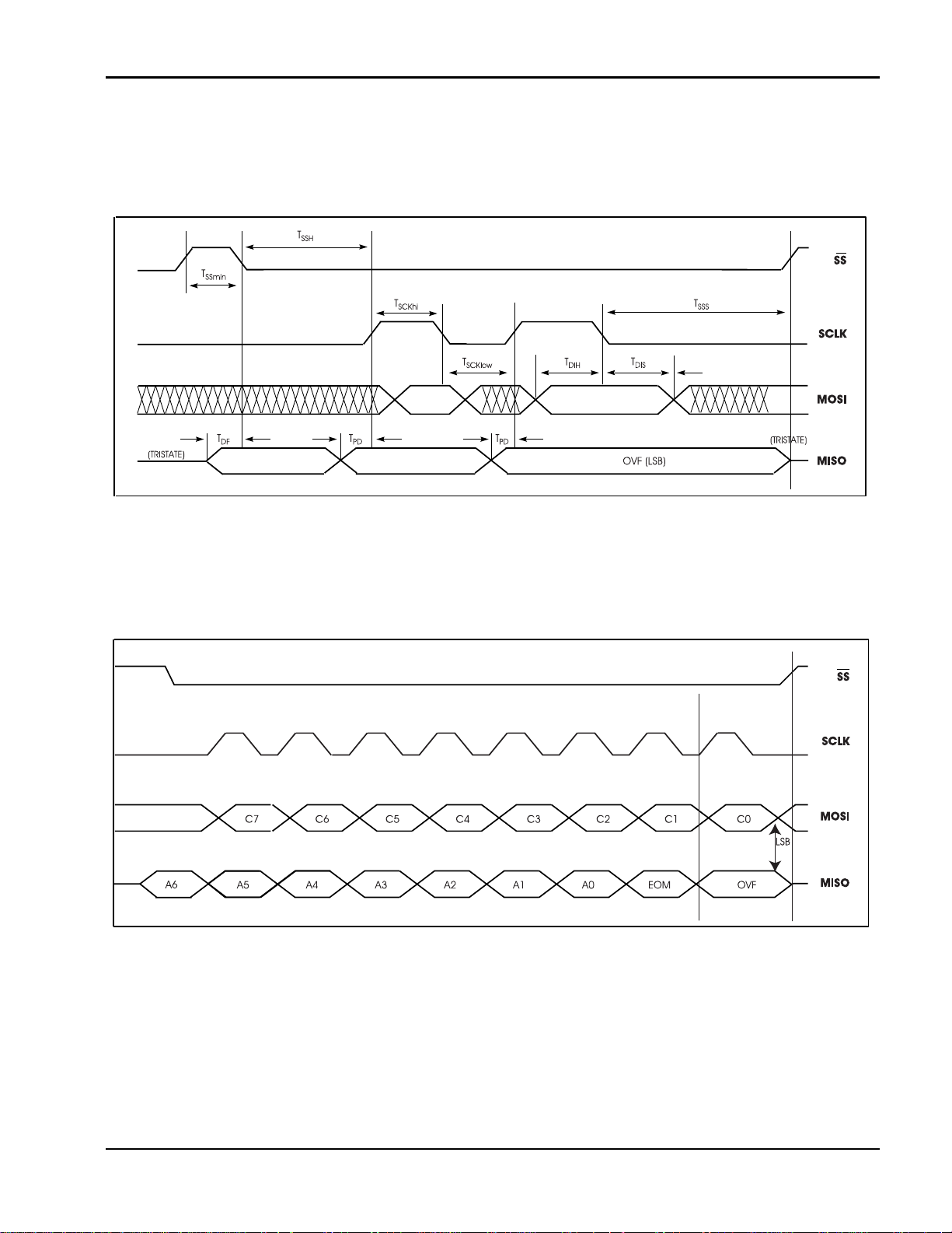
Figure 16: SPI Timing Diagram
Figure 17: 8-Bit SPI Command Format
ISD
31
Page 36
ISD5008 Product
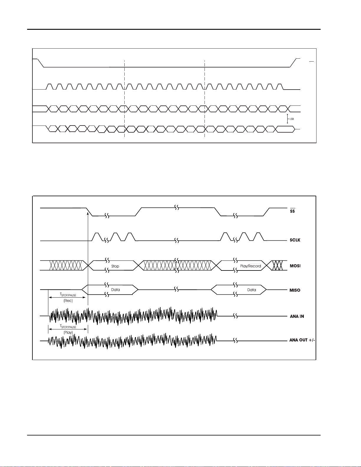
Figure 18: 24-Bit SPI Command Format
SS
BYTE 3BYTE 2BYTE 1
SCLK
C1 C0
C2
XXXXXX
A12A13A14A15
A11
D12D13D14D15C3C4C5C6C7
D6D7D8D9D10D11
A4A5A6A7A8A9 OVFEOMA0A1A2A3A10
Figure 19: Playback/Record and Stop Cycle
D0D1D2D3D4D5
MOSI
MISO
32
Voice Solutions in Silicon™
Page 37
7 DEVICE PHYSICAL DIMENSIONS
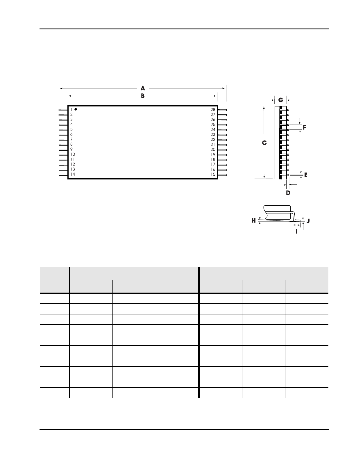
Figure 20: 28-Lead 8x13.4 mm Plastic Thin Small Outline Package (TSOP) Type I (E)
ISD5008 Product
Table 17: Plastic Thin Small Outline Package (TSOP) Type I (E) Dimensions
INCHES MILLIMETERS
Min Nom Max Min Nom Max
A 0.520 0.528 0.535 13.20 13.40 13.60
B 0.461 0.465 0.469 11.70 11.80 11.90
C 0.311 0.315 0.319 7.90 8.00 8.10
D 0.002 0.006 0.05 0.15
E 0.007 0.009 0.011 0.17 0.22 0.27
F 0.0217 0.55
G 0.037 0.039 0.041 0.95 1.00 1.05
H 0° 3° 6° 0° 3° 6°
I 0.020 0.022 0.028 0.50 0.55 0.70
J 0.004 0.008 0.10 0.21
NOTE: Lead coplanarity to be within 0.004 inches.
ISD
33
Page 38
ISD5008 Product
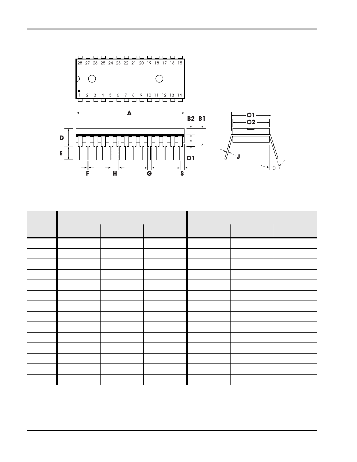
Figure 21: 28-Lead 0.600-Inch Plastic Dual Inline Package (PDIP) (P)
Table 18: Plastic Dual Inline Package (PDIP) (P) Dimensions
INCHES MILLIMETERS
Min Nom Max Min Nom Max
A 1.445 1.450 1.455 36.70 36.83 36.96
B1 0.150 3.81
B2 0.065 0.070 0.075 1.65 1.78 1.91
C1 0.600 0.625 15.24 15.88
C2 0.530 0.540 0.550 13.46 13.72 13.97
D 0.19 4.83
D1 0.015 0.38
E 0.125 0.135 3.18 3.43
F 0.015 0.018 0.022 0.38 0.46 0.56
G 0.055 0.060 0.065 1.40 1.52 1.65
H 0.100 2.54
J 0.008 0.010 0.012 0.20 0.25 0.30
S 0.070 0.075 0.080 1.78 1.91 2.03
q 0° 15° 0° 15°
34
Voice Solutions in Silicon™
Page 39
ISD5008 Product
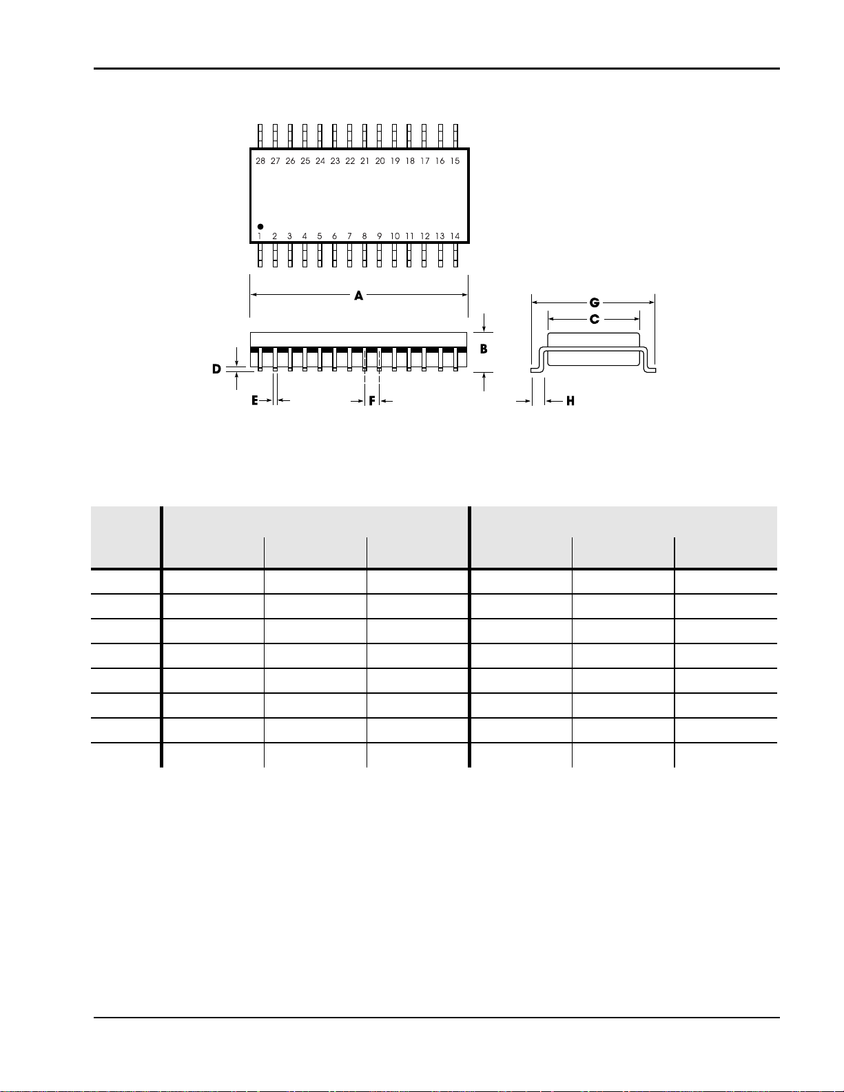
Figure 22: 28-Lead 0.300-Inch Plastic Small Outline Integrated Circuit (SOIC) (S)
Table 19: Plastic Small Outline Integrated Circuit (SOIC) (S) Dimensions
INCHES MILLIMETERS
Min Nom Max Min Nom Max
A 0.701 0.706 0.711 17.81 17.93 18.06
B 0.097 0.101 0.104 2.46 2.56 2.64
C 0.292 0.296 0.299 7.42 7.52 7.59
D 0.005 0.009 0.0115 0.127 0.22 0.29
E 0.014 0.016 0.019 0.35 0.41 0.48
F 0.050 1.27
G 0.400 0.406 0.410 10.16 10.31 10.41
H 0.024 0.032 0.040 0.61 0.81 1.02
NOTE: Lead coplanarity to be within 0.004 inches.
ISD
35
Page 40
ISD5008 Product
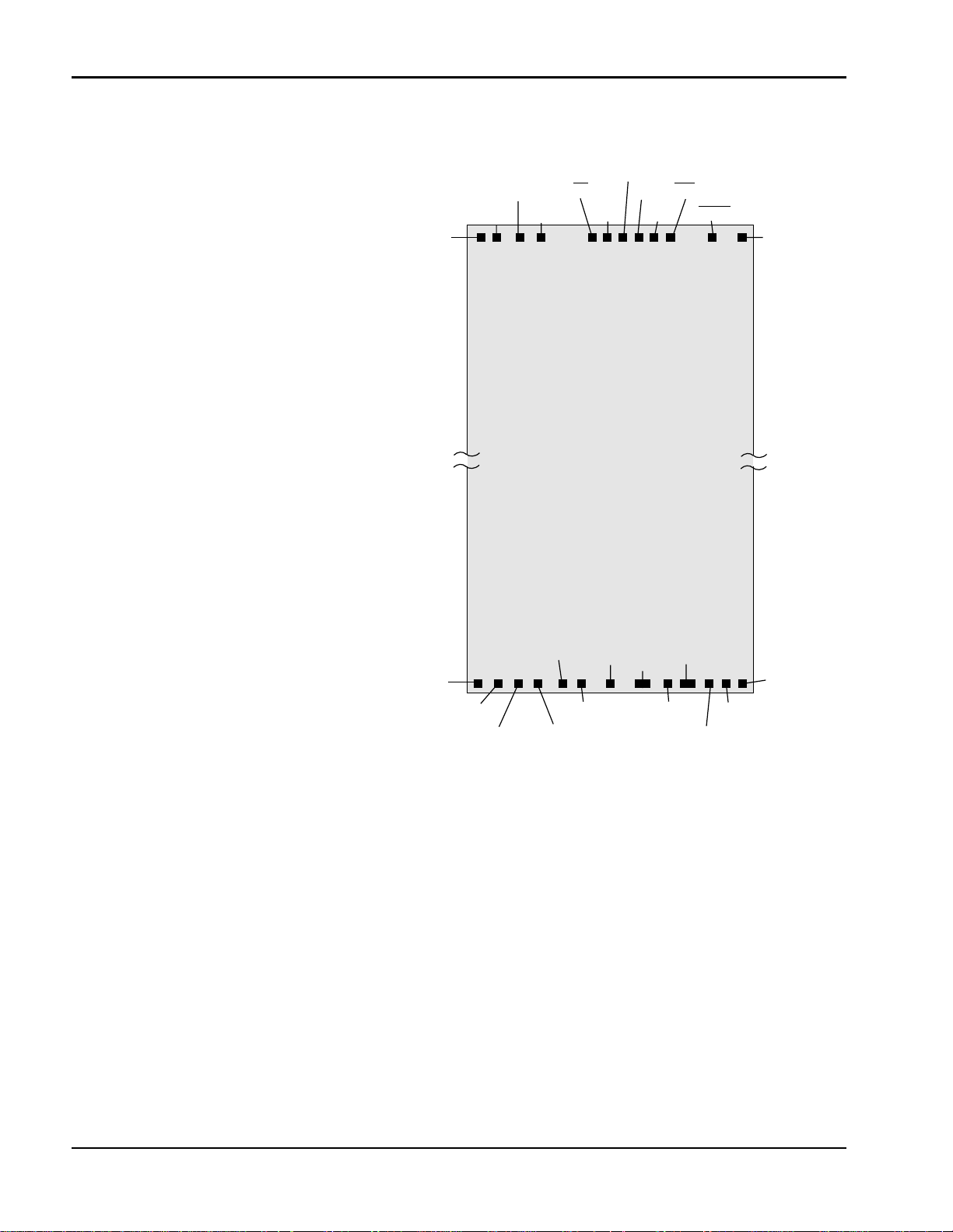
Figure 23: ISD5008 Series Bonding Physical Layout
ISD5008 Series
I. Die Dimensions
X: 166.5 ±1 mils
Y: 302.4 ±1 mils
II. Die Thickness
(3)
11.5 ±0.5 mils
III. Pad Opening (min)
90 x 90 microns
3.5 x 3.5 mils
(1)
(Unpackaged Die)
V
CCD
MISO
V
SSD
V
SSD
MOSI
SS
SCLK
V
CCD
XCLK
INT
RAC
V
SSA
ISD5008
ANAOUT–
V
SSA
MIC+ AUX IN
ACAP
SP– V
(2)
V
SSA
SP+
CCA
(2)
AUXOUT
ANA INANAOUT+MIC–
1. The backside of die is internally connected to VSS. It MUST NOT be connected to any other potential or damage
may occur.
2. Double bond recommended.
3. This figure reflects the current die thickness. Please contact ISD as this thickness may change in the future.
36
Voice Solutions in Silicon™
Page 41
ISD5008 Product
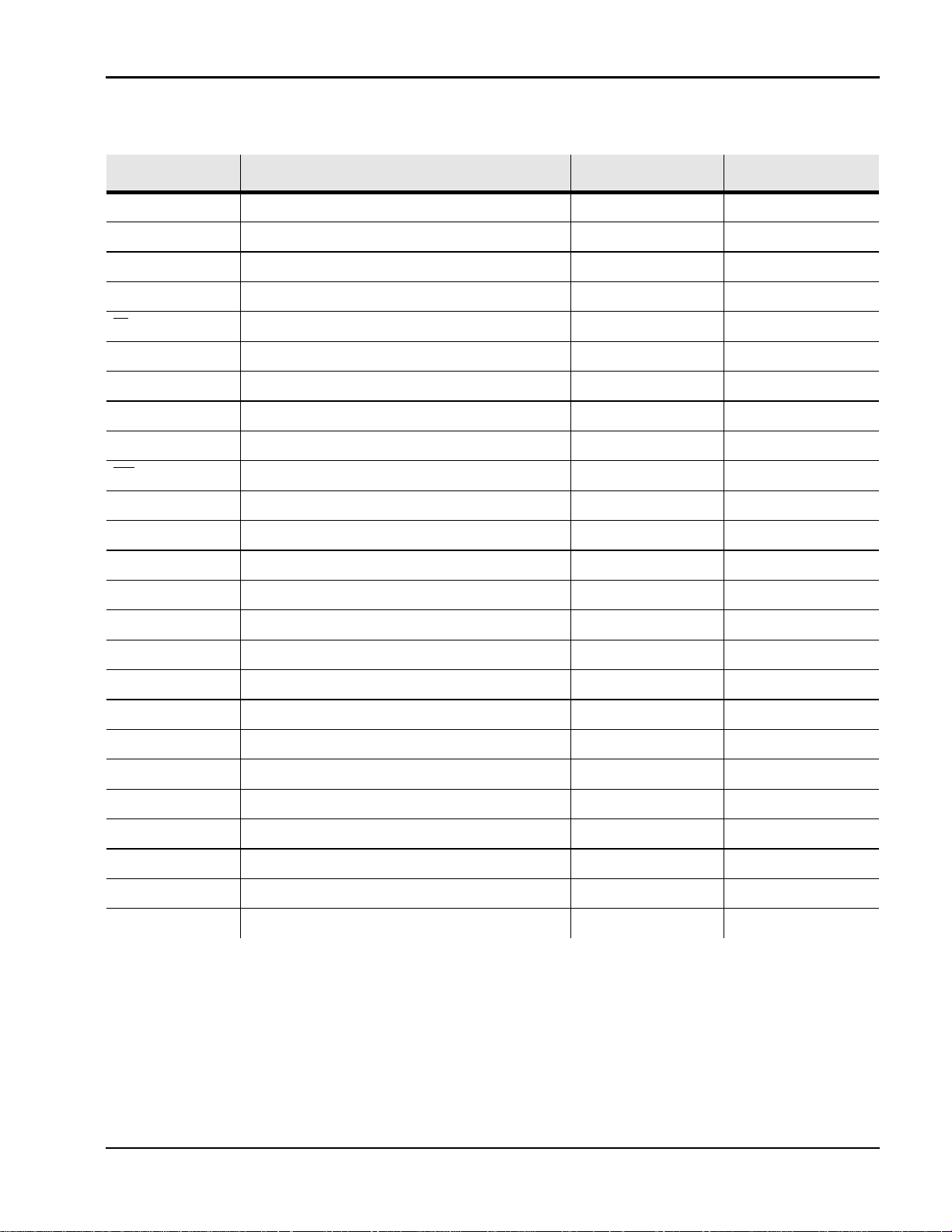
Table 20: ISD5008 Series Device Pin/Pad Designations,
with Respect to Die Center (µm)
Pin Pin Name X Axis Y Axis
V
SSD
V
SSD
VSS Digital Power Supply –1837.0 3623.7
VSS Digital Power Supply –1665.4 3623.7
MISO Master In Slave Out –1325.7 3623.7
MOSI Master Out Slave In –1063.8 3623.7
SS Slave Select –198.2 3623.7
SCLK Slave Clock –14.8 3623.7
V
V
CCD
CCD
VCC Digital Power Supply 169.4 3623.7
VCC Digital Power Supply 384.8 3623.7
XCLK External Clock Input 564.7 3623.7
INT Interrupt 794.7 3623.7
RAC Row Address Clock 1483.7 3623.7
V
SSA
V
SSA
VSS Analog Power Supply 1885.1 3623.7
VSS Analog Power Supply –1943.2 –3615.9
MIC+ Noninverting Microphone Input –1735.4 –3615.9
MIC– Inverting Microphone Input –1502.9 –3615.9
ANA OUT+ Noninverting Analog Output —1251.2 –3615.9
ANA OUT – Inverting Analog Output –917.0 –3615.9
ACAP AGC/AutoMute Cap –632.6 –3615.9
SP– Inverting Speaker Output –138.4 –3615.9
(1)
V
SSA
VSS Analog Power Supply 240.2 –3615.9
SP+ Noninverting Speaker Output 618.8 –3615.9
(1)
V
CCA
VCC Analog Power Supply 997.4 –3615.9
ANA IN Analog Input 1249.9 –3615.9
AUX IN Auxiliary Input 1515.5 –3615.9
AUX OUT Auxiliary Output 1758.4 –3615.9
1. Double bond recommended.
ISD
37
Page 42
ISD5008 Product
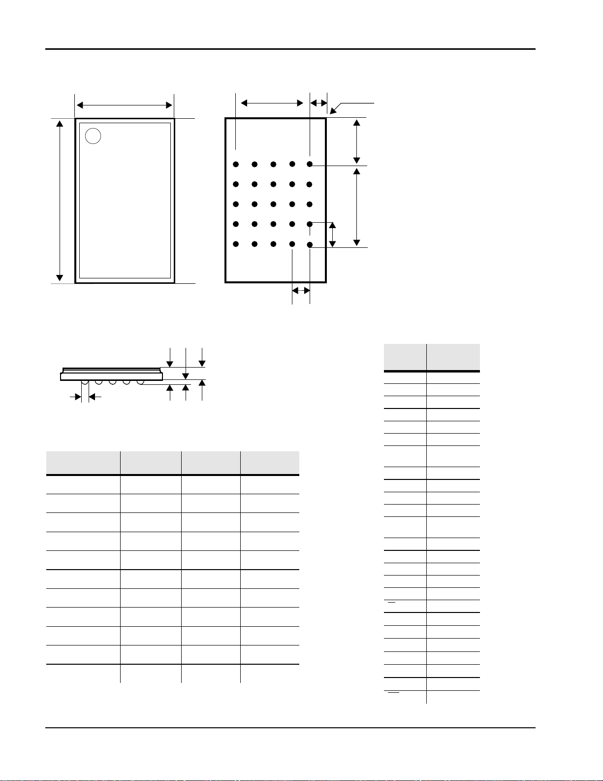
Figure 24: SD5008 Chip Scale Package (CSP) (Z)
C
B5 B4 B3 B2
D
C5 C4 C3 C2
D5 D4 D3 D2
E5 E4 E3 E2
TOP VIEW
2
1
AA
A
b
SIDE VIEW
Table 21: CSP Dimensions (mm)
Symbol Min. Nom. Max.
A — — 0.86
1
A
2
A
b 0.30 0.35 0.40
C — 4.68 —
D — 8.13 —
e 0.75
F — 3.00 —
G — 0.84 —
H — 2.57 —
I — 3.00 —
0.18 — —
— 0.55 —
F
A5 A4 A3
BOTTOM VIEW
A2
G
A1
B1
C1
D1
E1
e
e
A1 Ball Corner
H
I
Name
MIC- A1
ACAP A2
V
SSA
V
CCA
AUX IN A5
MIC+ B1
ANA
OUTSP- B3
ANA IN B4
AUX OUT B5
V
SSA
ANA
OUT
SP+ C3
V
CCD
V
SSA
V
SSD
MISO D2
SS
XCLK
RAC D5
VSSD E1
MOSI E2
SCLK E3
VCCD E4
INT
PIN
+
Ball
Location
A3
A4
B2
C1
C2
C4
C5
D1
D3
D4
E5
38
Voice Solutions in Silicon™
Page 43
8 ORDERING INFORMATION
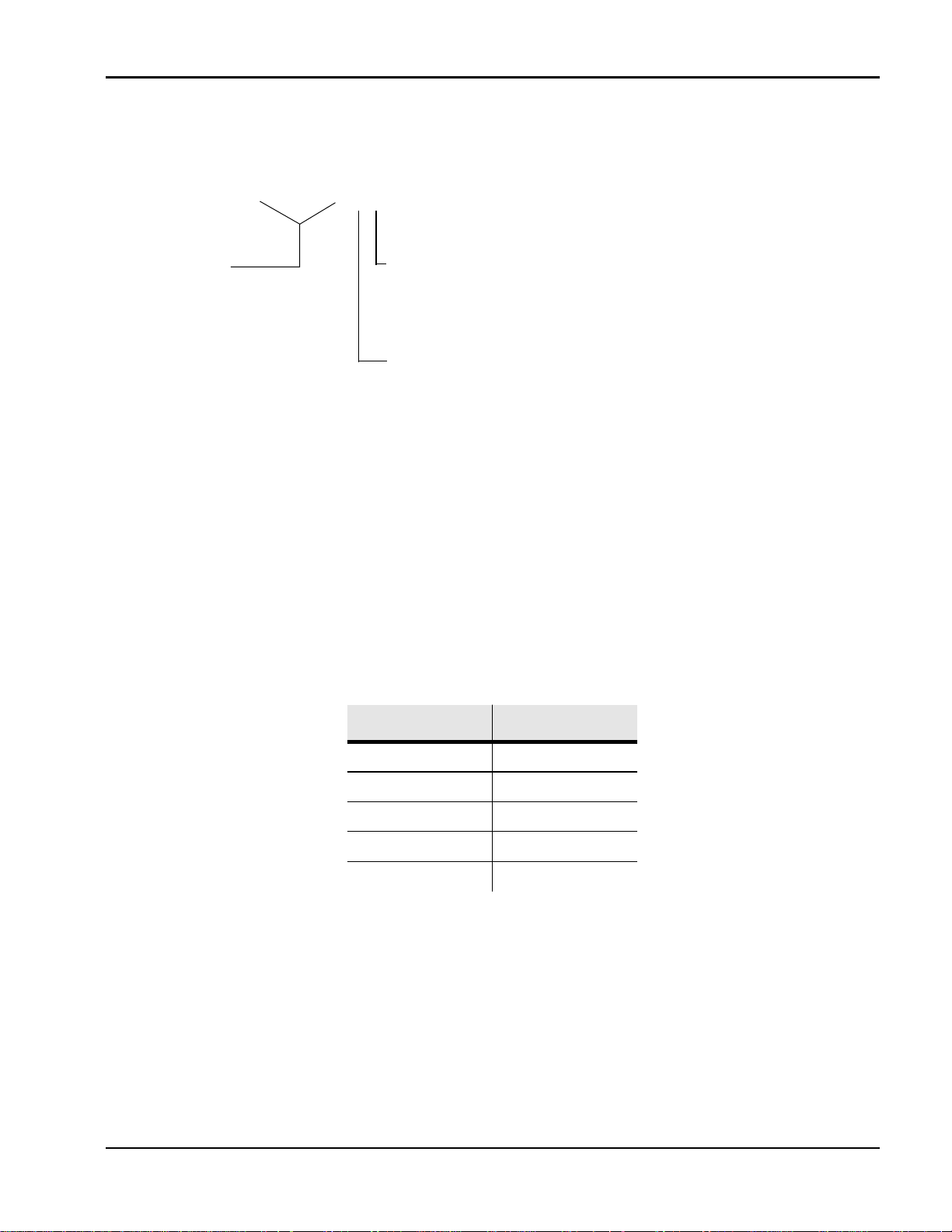
ISD Part Number Description
ISD5008–_ _
ISD5008 Product
Product Family
ISD5008 Product
(4 to 8 minute
durations)
Special Temperature Field:
Blank= Commercial Packaged (0˚C to +70˚C)
or Commercial Die (0˚C to +50˚C)
I = Industrial (–40˚C to +85˚C)
Package Type:
E = 28-Lead 8x13.4mm Plastic Thin Small Outline
Package (TSOP) Type 1
P = 28-Lead 0.600-Inch Plastic Dual Inline
Package (PDIP)
S = 28-Lead 0.300-Inch Plastic Small Outline
Package (SOIC)
X = Die
Z = Chip Scale Package (CSP)
When ordering ISD5008 series devices, please refer to the following valid part numbers.
Part Number Part Number
ISD5008E ISD5008X
ISD5008EI ISD5008Z
ISD5008P ISD5008ZI
ISD5008S
ISD5008SI
For the latest product information, access ISD’s worldwide website at http://www.isd.com.
ISD
39
Page 44

ISD5008 Product
40
Voice Solutions in Silicon
™
Page 45

IMPORTANT NOTICES
The warranty for each product of ISD (Information Storage
Devices, Inc.), is contained in a written warranty which governs
sale and use of such product. Such warranty is contained in the
printed terms and conditions under which such product is sold, or
in a separate written warranty supplied with the product. Please
refer to such written warranty with respect to its applicability to
certain applications of such product.
These Product may be subject to restrictions on use. Please
contact ISD, for a list of the current additional restrictions on
these Product. By purchasing these Product, the purchaser of
these Product agrees to comply with such use restrictions. Please
contact ISD for clarification of any restrictions described herein.
ISD, reserves the right, without further notice, to change the ISD
ChipCorder product specifications and/or information in this
document and to improve reliability, functions and design.
ISD assumes no responsibility or liability for any use of the ISD
ChipCorder Product. ISD conveys no license or title, either
expressed or implied, under any patent, copyright, or mask work
right to the ISD ChipCorder Product, and ISD makes no warranties
or representations that the ISD ChipCorder Product are free from
patent, copyright, or mask work right infringement, unless
otherwise specified.
Application examples and alternative uses of any integrated
circuit contained in this publication are for illustration purposes
only and ISD makes no representation or warranty that such
applications shall be suitable for the use specified.
The 100-year retention and 100K record cycle projections are
based upon accelerated reliability tests, as published in the ISD
Reliability Report, and are neither warranted nor guaranteed by
ISD.
Information contained in this ISD ChipCorder data sheet
supersedes all data for the ISD ChipCorder Product published by
ISD prior to December, 1998.
This data sheet and any future addendum to this data sheet is
(are) the complete and controlling ISD ChipCorder product
specifications. In the event any inconsistencies exist between the
information in this and other product documentation, or in the
event that other product documentation contains information in
addition to the information in this, the information contained
herein supersedes and governs such other information in its entirety.
Copyright© 1999, ISD (Information Storage Devices, Inc.) All rights
reserved. ISD is a registered trademark of ISD. ChipCorder is a
trademark of ISD. All other trademarks are properties of their
respective owners.
A Winbond Company
®
2727 North First Street
San Jose, California 95134
Tel: 408/943-6666
Fax: 408/544-1787
http://www.isd.com
Part No. ISD5008PDS1-799
 Loading...